1
Rev. 09/18/02 SPX4040 Micropower 2.5V Shunt Voltage Reference
© Copyright 2002 Sipex Corporation
Precision Micropower 2.5V ShuntVoltage Reference
The SPX4040 is a 2-terminal, temperature compensated, bandgap voltage reference that
provides a fixed 2.5V output for input currents between 160
µ
A and 15mA. The bandgap voltage
(2.5V) is independently trimmed from the output voltage to achive a very low temperature
coefficient. This trimming technique gives a stable device over the full temperature range
(100ppm/
∞
C).
The SPX4040 is available in TO-92, SOIC-8 and SOT-23-3 packages. The operating tempera-
ture range is -40
∞
C to 85
∞
C. The SPX4040 advanced design eliminates the need for an external
stabilizing capacitor while ensuring stability with any capacitive load, making it easy to use.
SPX4040
Æ
FEATURES
Trimmed Bandgap to 0.5% and 1%
Wide Operating Current 160
µ
A to 15mA
Extended Temperature Range:
-40
∞
C to 85
∞
C
Low Temperature Coefficient 100 ppm/
∞
C
Offered in TO-92, SOIC, SOT-23-3
Replacement in for LM4040
APPLICATIONS
Battery Operating Equipment
Adjustable Supplies
Switching Power Supplies
Error Amplifiers
Single Supply Amplifier
Monitors / VCRs / TVs
Personal Computers
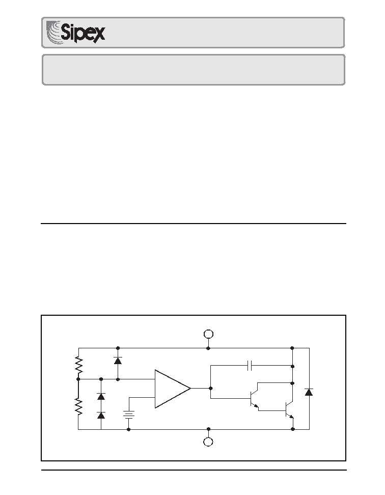
DESCRIPTION
Anode (A)
Cathode (K)
2.5V
+
-
R
R

2
Rev. 09/18/02 SPX4040 Micropower 2.5V Shunt Voltage Reference
© Copyright 2002 Sipex Corporation
ABSOLUTE MAXIMUM RATINGS
Anode-Cathode Forward Current, (<10ms)
I
AK
............................. 10mA
Anode-Cathode Reverse Current I
KA
........................................... 20mA
Continuous Power Dissipation at 25
∞
C P
D
TO-92 ..................................................................... 550mW
SOT-23 .................................................................. 300 mW
SOIC-8 .................................................................... 525mW
Junction Temperature T
J
........................................................... 150
∞
C
Storage Temperature T
STG
.............................................. -65 to 150
∞
C
Lead Temperature (Soldering 5 sec.) T
L
.................................... 300
∞
C
NOTE: Stresses greater than those listed under ABSOLUTE MAXIMUM
RATINGS may cause permanent damage to the device. This is a stress
rating only and functional operation of the device at these or any other
conditions above those indicated in the operational sections of this
specification is not implied. Exposure to absolute maximum rating condi-
tions for extended periods may affect reliability.
TYPICAL THERMAL RESISTANCES
PACKAGE
0
JA
0
JC
TYPICAL DERATING
TO-92
160
∞
C/W 80
∞
C/W
6.3 mW/
∞
C
SOT-23
575
∞
C/W 150
∞
C/W
1.7 mW/
∞
C
SOIC-8
175
∞
C/W 45
∞
C/W
5.7 mW/
∞
C
Typical deratings of the thermal resistances are given for ambient
temperature >25
∞
C.
PARAMETERS
CONDITIONS
MIN
TYP
MAX
MIN
TYP
MAX
UNITS
SPX4040A-2.5
SPX4040-2.5
Reverse Breakdown
I
R
= 500
µ
A
2.4875
2.500 2.5125
2.475
2.500
2.525
V
Voltage
Reverse Breakdown
I
R
= 500
µ
A
±
12
±
25
mV
Tolerance
-40
∞
C < T
A
< 85
∞
C
±
29
±
49
mV
Output Impedance
0.60
0.8
0.60
0.8
Noise Voltage
0.1KHz
f
10Hz
15
15
µ
V p-p
Tempco
Note 1
100
100
ppm/
∞
C
Turn-on Setting
1.0% of V
OUT
30
30
µ
Sec
Operating Current Range Note 2
0.16
15
0.16
15
mA
Temp. Range (ambient)
-40
85
-40
85
∞
C
0
75
85
-10
0.5
5000
0
0
0
0.07 mV/
∞C
0.003 %/
∞C
27 ppm/
∞C
TC in mV/
∞C =
TC in % /
∞C =
(mV)
T
A
T
A
at 25
∞C
x 100
(
)
TC in ppm/
∞C =
at 25
∞C
x 10
6
(
)
ppm
%
mV
Junction Temperature (
∞C)
T
V
KA
V
KA
V
KA
V
KA
V
KA
V
KA
T
A
15
45
60
30
CALCULATING AVERAGE TEMPERATURE COEFFICIENT (TC)
Figure 1. V
KA
VS Temperature.
Notes:
1. Three-point measurement guarantees the error band over the specified temperature range.
2. Optimum performance is obtained at current below 1000
µA.
ELECTRICAL CHARACTERISTICS
Electrical characteristics at I
N
= 1000
µA and T
A
= +25
∞C unless otherwise specified.

3
Rev. 09/18/02 SPX4040 Micropower 2.5V Shunt Voltage Reference
© Copyright 2002 Sipex Corporation
TYPICAL PERFORMANCE CHARACTERISTICS
V
IN
V
KA
I
K
-2
-1
0
1
2
3
150
125
100
75
50
25
0
-25
-50
-75
-100
V
KA
Cathode Voltage (V)
I
K
Cathode Current (mA)
V
KA
= 2.5V
0
∞
C to 85
∞
C
Figure 2. Test Circuit for I
KREVERSE,
V
KA
= 2.5V
Figure 3. High Current Operating Characteristics
-1.0
0
1.0
2.0
3.0
270
240
210
180
150
120
90
60
30
0
-30
-60
V
KA
Cathode Voltage (V)
I
K
Cathode Current (
µ
A)
V
KA
= 2.5V
0
∞
to 105
∞
C
105
∞
C
25
∞
C
-0
∞
C
Figure 4. Low Current Operating Characteristics
Figure 5. Noise Voltage VS Frequency
Z
KA
Dynamic Impedance (
)
TA - Free Air Temperature
V
KA
= 2.5V
I
KA
= 1 to 15mA
f
1kHz
0.150
0.125
0.100
0.075
0.050
0.025
0.0
-60
-30
0
30
60
85
Figure 7. Frequency = 100kHz, I
K
= 10mA, T
A
= 25
∞C
V
OUT
V
IN
Noise V
oltage nV/
Hz
f Frequency (Hz)
V
KA
= 2.5V
I
K
= 10mA
T
A
= 25
∞
C
70
60
50
40
30
20
10
0
10
100
1K
10K
100K
Figure 6. Low Frequency Dynamic Output Impedance
VS. T
AMBIENT

4
Rev. 09/18/02 SPX4040 Micropower 2.5V Shunt Voltage Reference
© Copyright 2002 Sipex Corporation
TYPICAL PERFORMANCE CHARACTERISTICS (continued)
Figure 10. Off State Leakage
I
K
V
OUT
GND
250
50
V
IN
f
p = 100kHz
Figure 8. Test Circuit for Pulse Response
T
A
= 25
∞
C
I
K
=1 to 15mA
Z
KA
Dynamic Impedance (
)
f Frequency (Hz)
100
10
1.0
0.1
0.01
1K
10K
100K
1M
10M
Figure 9. Dynamic Output Impedance T
A
= 25
∞C,
I
K
= 1 to 15mA
0.01
0.1
1
10
100
-50
0
50
100
150
T
A
Ambient Temperature (
∞
C)
I
KOFF
Cathode Current
V
KA
= 2.5V
APPLICATION INFORMATION
This device is designed for stable operation and
has no need of an external capacitor between
pins 4 and 8. The reference remains stable if a
bypass capacitor is used.
SOT-23
The SPX4040 in the SOT-23 package has a
parasitic Schottky diode between pin 3 and pin
1. Pin 1 of SOT-23 must float or be connected
to pin 3.
Conventional Shunt Regulator
In a conventional shunt regulator application
(see Figure 11), an external series resistor (R
S
) is
connected between the supply voltage and the
SPX4040. R
S
determines the current that flows
through the load (I
L
) and the reference (I
Q
).
Since load current and supply voltage may vary,
R
S
should be small enough to supply at least the
minimum acceptable I
Q
to the reference even
when the supply voltage is at its minimum and
the load current is at its maximum value. When
the supply voltage is at its maximum and I
L
is at
its minimum, R
S
should be large enough so that
the current flowing through the SPX4040 is less
than 15mA.
R
S
is determined by the supply voltage (V
S
), the
load and operating current (I
L
and I
Q
), reference's
reverse breakdown voltage (V
R
).
R
S
= (V
S
-V
R
)/(I
L
+I
Q
)

5
Rev. 09/18/02 SPX4040 Micropower 2.5V Shunt Voltage Reference
© Copyright 2002 Sipex Corporation
V
S
RS I
Q
+ I
L
SPX4040
V
OUT
I
L
I
Q
V
R
LM4250C
1M
V
IN
= 15V
10V
+
_
1.17M
3.5M
22M
150pF
7
8
6
4
3
2
I
Q
SPX4040-2.5
I
Q
2
µ
A standby current
Figure 11. SPX4040 Fixed Shunt Regulator Application
Figure 12. Micropower 10V Reference
LM312
R1
100k
≠
+
R2
C1
150pF
7
6
4
3
2
SPX4040-2.5
30V
I
OUT
*
2.5V to 27V
* I
OUT
= 5.0V
R2
3k
3.0V
SPX4040-2.5
2.5V
Figure 13. Precision 1
µA to mA Current Source
Figure 14. Reference from 3.0V Battery
4.3k
V
IN
= 3.3V to 30V
SPX4040-2.5
2.5V
LM334
Figure 15. Wide Input Range Reference