
Rev. 11/21/00
SPX432
Ultra 1.24V Precision Adjustable
Shunt Regulator
FEATURES APPLICATIONS
∑ Low Voltage Operation........................................ 1.24V
∑ 3.0V to 3.3V Switching Power Supplies
∑ Trimmed Bandgap to ...................................0.5%/ 1%
∑ Adjustable Supplies
∑ Wide Operating Current ................... 1mA to 100mA
∑ Error Amplifiers
∑ Extended Temperature Range ...............0∞∞∞∞C to 105∞∞∞∞C
∑ Single Supply Amplifier
∑ Adjustable Output Voltage...........................V
REF
to 18V
∑ Monitors / VCR / TV
∑ Low Temperature Coefficient ....................... 50 ppm/∞C
∑ Personal Computers
∑ Offered in TO-92, SOIC, SOT-23-3, SOT-23-5
∑ Improved Replacement in Performance for TLV431
PRODUCT DESCRIPTION
The SPX432 is a 3-terminal Adjustable Shunt Voltage Regulator providing a highly accurate 1.24V bandgap reference with 0.5%
tolerance. The SPX432 thermal stability, wide operating current (80mA) and temperature range (0
∞C to 105∞C) makes it suitable for
abroad range of applications. SPX432 tolerance of 0.5% is proven to be sufficient to overcome other errors in the system to
virtually eliminate the need for trimming in the power supply manufactures assembly line and contribute a significant cost
savings.
The SPX432 is an ideal voltage reference in an isolated feedback circuit for 3.0V to 3.3V switching mode power supplies. SPX432
offers many advantages over TLV431, such as, wider output voltage up to 18V vs. 6V, output current of 80mA vs. 15mA, and a wider
temperature range with tighter tolerance down to 0.5%.
Top View
2
1
3
4
8
7
6
5
SPX432
8-Pin Surface Mount (S)
Bottom View
TO-92 (N)
1
3
2
CATHODE
ANODE
ANODE
N/C
REF
ANODE
ANODE
N/C
REF
ANODE
CATHODE
Top View
SPX432
SOT-23-3 (M)
Top View
SPX432
SOT-23-5 (M5)
ANODE
REF
CATHODE
ANODE
REF
N/C
N/C CATHODE
PIN CONNECTIONS

Rev. 11/21/00
SPX432
ABSOLUTE MAXIMUM RATINGS
Parameter Symbol
Rating
Units
Cathode-Anode Reverse Breakdown
V
DA
18 V
Anode-Cathode Forward Current
I
AK
1 A
Operating Cathode Current
I
KA
80 mA
Reference Input Current
I
REF
1 mA
Continuous Power at 25
∞C
TO-92
8L SOIC
SOT-23
P
D
775
750
200
mW
mW
mW
Junction Temperature
T
J
150 ∞C
Storage Temperature
T
STG
- 65 to +150
∞C
Lead Temperature (Soldering 10 sec.)
TL
300
∞C
Stresses greater than those listed under ABSOLUTE MAXIMUM RATINGS may cause permanent damage to the device. This is a stress rating only and functional
operation of the device at these or any other conditions above those indicated in the operational sections of this specification is not implied. Exposure to absolute
maximum rating conditions for extended periods may affect reliability.
RECOMMENDED CONDITIONS TYPICAL THERMAL RESISTANCES
Parameter Symbol
Rating
Unit
Package
JA
JC
Typical Derating
Cathode Voltage
V
KA
V
REF
to 18
V
TO-92
160
∞C/W 80
∞C/W 6.3
mW/
∞C
Cathode Current
I
K
10
mA
SOIC 175 ∞C/W 45
∞C/W 5.7
mW/
∞C
SOT-23
575
∞C/W 150∞C/W 1.7mW/∞C
1.24V
+
-
REFERENCE
(R)
CATHODE (K)
ANODE (A)

Rev. 11/21/00
ppm
mV
TC in mV/∞C =
V
REF
(mV)
T
A
TC in %/∞C =
V
REF
at 25∞C
T
A
V
REF
)
)
x 100
TC in ppm/∞C =
V
REF
at 25∞C
T
A
V
REF
)
)
x 10
6
5000
-55
0.06 mV/∞C
V
REF
0
0
0
%
-20
-10
0.5
Temperature (∞C)
0.002 %/∞C
24 ppm/∞C
-25
0
25
50
75 100 125
I
K
I
REF
V
IN
V
KA
= V
REF
V
IN
V
KA
I
K
R
1
R
2
(V
REF
)
Figure 1b. Test Circuit 2
Figure 1a. Test Circuit 1
V
IN
V
KA
I
K (OFF)
Figure 1c. Test Circuit 3
I
REF
SPX432
ELECTRICAL CHARACTERISTICS
are guaranteed over the full junction temperature range (0
∞C to 105∞C). Ambient
temperature must be derated based upon power dissipation and package thermal characteristics. Unless otherwise specified, test
conditions are: V
KA
= V
REF
and I
K
= 10mA.
Test
SPX432A SPX432
Parameter
Symbol Circuit
Test
Condition
Min Typ Max Min Typ Max Unit
Output Voltage
V
REF
1
1
I
K
= 10mA,
T
J
= 25
∞C,
V
K
= V
REF
1.2338 1.240 1.2462 1.2276 1.240 1.2524
V
Line Regulation
V
REF
1
V
KA
= 1.25V to 15V
19
37
19
37
mV
Load Regulation
V
REF
1
I
K
= 1 to 80mA
3
6
3
6
mV
Temperature Deviation
V
REF
1
0 < T
J
< 105
∞C
2 6 2 6
mV
Reference Input Current
I
REF
2
3 6 3 6
µA
Reference Input Current
Temperature Coefficient
I
REF
2
0 < T
J
< 105
∞C
0.3 0.6 0.3
0.6
µA
Minimum Cathode
Current for Regulation
I
K (MIN)
1
0.6 1 0.6 1
mA
Off State Leakage
I
K (MIN)
3
V
REF
= 0V, V
KA
=
18V
0.04 500 0.04
500
nA
Calculating Average Temperature Coefficient (TC)
TEST CIRCUITS
Rev. 11/21/00
SPX432
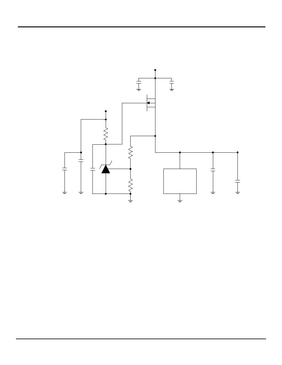
TYPICAL APPLICATIONS
INTEL
I 740
+3.3V
470µF
0.1µF
PHD 3055E
2.7V
+12V
0.1µF
AS432
120
140
500
0.1µF
1000µF
0.1µF
*If the output voltage has noise, then please add a 0.1
µF in between drain and gate of power
MOSFET to reduce the noise.
