1
Product Description
EDS-103299 Rev B
The information provided herein is believed to be reliable at press time. Sirenza Microdevices assumes no responsibility for inaccuracies or omissions. Sirenza Microdevices assumes no responsibility for the use of
this information, and all such information shall be entirely at the user's own risk. Prices and specifications are subject to change without notice. No patent rights or licenses to any of the circuits described herein are
implied or granted to any third party. Sirenza Microdevices does not authorize or warrant any Sirenza Microdevices product for use in life-support devices and/or systems. Copyright 2001 Sirenza Microdevices, Inc..
All worldwide rights reserved.
303 South Technology Court Phone: (800) SMI-MMIC http://www.sirenza.com
Broomfield, CO 80021
Symbol
Parameter
Units Frequency
M in.
T yp.
M ax.
G
p
Small Signal Power Gain [2]
dB
dB
dB
dB
dB
850 MHz
1950 MHz
2400 MHz
6000 MHz
10000 MHz
10.7
8.8
12.5
12.2
12.0
12.5
10.3
13.7
11.8
G
F
Gain Ripple
dB
0.1-8 GHz
+/- 0.5
BW 3dB 3dB Bandwidth
GHz
10.5
P
1dB
Output Power at 1dB Compression [2]
dBm
dBm
1950 MHz
10000 MHz
9
9.5
11.0
11.5
OIP
3
Output Third Order Intercept Point [2]
dBm
dBm
1950 MHz
10000 MHz
21
21
24.0
24.0
NF
Noise Figure
dB
1950 MHz
5
RL
Input / Output Return Loss
dB
1950 MHz
13
ISOL
Reverse Isolation
dB
0.1-10 GHz
16
V
D
Device Operating Voltage [1]
V
3.1
3.6
4.1
I
D
Device Operating Current [1]
mA
35
40
45
dG/dT
Device Gain Temperature Coefficient
dB/�C
-0.0015
R
TH
, j-b Thermal Resistance (junction to backside)
�C/W
280
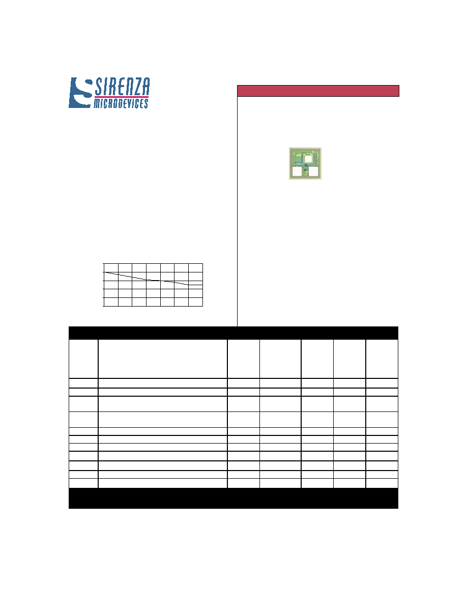
Sirenza Microdevices' SNA-100S is a GaAs monolithic
broadband amplifier (MMIC) in die form. This amplifier
provides 12.2dB of gain at 1950 MHz and 10.3dB at
10,000 MHz.
These unconditionally stable amplifiers are designed for use
as general purpose 50 ohm gain blocks. Its small size
(0.350mm x 0.345mm) and gold metallization make it an
ideal choice for use in hybrid circuits. The SNA-100S is
100% DC tested and sample tested for RF performance.
External DC decoupling capacitors determine low frequency
response. The use of an external resistor allows for bias
flexibility and stability.
The SNA-100S is supplied in gel paks of 100 devices.
Also available in packaged form (SNA-176 & SNA-186)
SNA-100S
DC-10 GHz, Cascadable
GaAs HBT MMIC Amplifier
Product Features
�
Cascadable 50 Ohm Gain Block
�
12.2dB Gain, +11dBm P1dB
�
1.5:1 Input and Output VSWR
�
Operates From Single Supply
�
Through wafer via for ground
Applications
�
Broadband Driver Amplifier for Fiber & CATV
transmitters
�
IF Amplifier or gain stage for VSAT, LMDS,
WLAN, and Cellular Systems
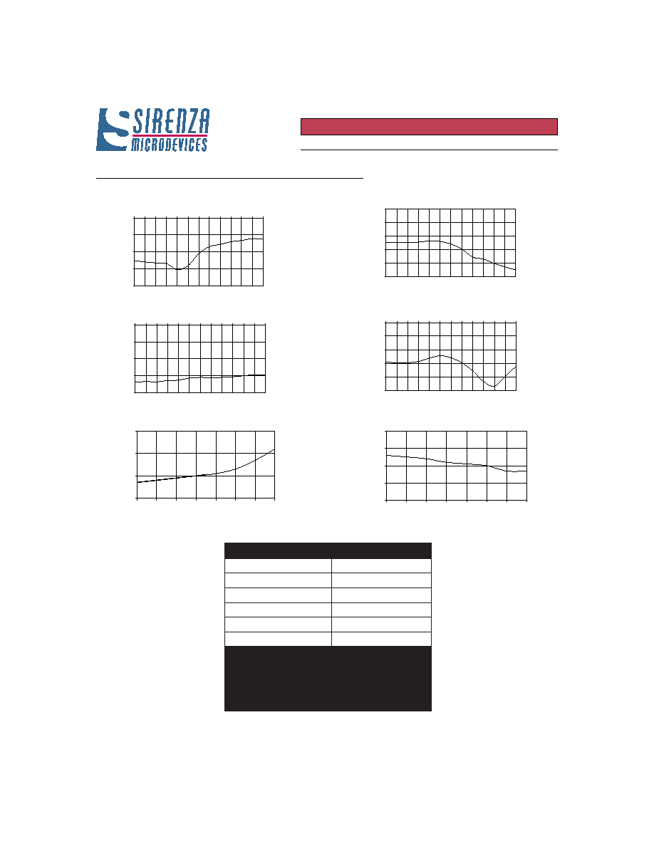
Output Power vs. Frequency
8
9
10
11
12
13
0.5
1
1.5
2
4
6
8
10
GHz
dBm
Test Conditions:
V
S
= 8 V
I
D
= 40 mA Typ.
OIP
3
Tone Spacing = 1.2 MHz, Pout per tone = 0 dBm
R
BIAS
= 110 Ohms
T
L
= 25�C, Z
S
= Z
L
= 50 Ohms, [1] 100% DC Tested, [2] Sample Tested
2
EDS-103299 Rev B
Preliminary
SNA-100S DC-10 GHz Cascadable MMIC Amplifier
303 South Technology Court Phone: (800) SMI-MMIC http://www.sirenza.com
Broomfield, CO 80021
Noise Figure vs. Frequency
5
6
7
8
0.5
1
1.5
2
4
6
8
10
dB
GHz
22
23
24
25
26
0.5
1
1.5
2
4
6
8
10
|S11| vs. Frequency
|S21| vs. Frequency
|S12| vs. Frequency
|S22| vs. Frequency
TOIP vs. Frequency
-20
-15
-10
-5
0
0.5
1
1.5
2
4
6
8
10
12
14
16
18
20
-20
-15
-10
-5
0
0.5
1
1.5
2
4
6
8
10
12
14
16
18
20
0
5
10
15
20
25
0.5
1
1.5
2
4
6
8
10
12
14
16
18
20
-25
-20
-15
-10
-5
0
0.5
1
1.5
2
4
6
8
10
12
14
16
18
20
dB
GHz
Typical Performance at 25
��
��
�
C (Vds =3.8V, Ids = 40mA)
(data includes bond wires)
dB
GHz
dBm
GHz
dB
GHz
dB
GHz
Absolute Maximum Ratings
r
e
t
e
m
a
r
a
P
t
i
m
i
L
e
t
u
l
o
s
b
A
.
x
a
M
t
n
e
r
r
u
C
e
c
i
v
e
D
I
(
D
)
0
9
A
m
.
x
a
M
e
c
i
v
e
D
V
(
e
g
a
tl
o
V
D
)
V
6
.
x
a
M
r
e
w
o
P
t
u
p
n
I
F
R
m
B
d
0
2
+
.
x
a
M
p
m
e
T
n
o
it
c
n
u
J
T
(
.
J
)
+
0
0
2
C
�
p
m
e
T
g
n
it
a
r
e
p
O
T
(
e
g
n
a
R
.
L
)
C
�
5
8
+
o
t
C
�
0
4
-
.
x
a
M
p
m
e
T
e
g
a
r
o
t
S
.
C
�
0
5
1
+
y
a
m
s
ti
m
il
e
s
e
h
t
f
o
e
n
o
y
n
a
d
n
o
y
e
b
e
c
i
v
e
d
s
i
h
t
f
o
n
o
it
a
r
e
p
O
,
n
o
it
a
r
e
p
o
s
u
o
n
it
n
o
c
e
l
b
a
il
e
r
r
o
F
.
e
g
a
m
a
d
t
n
e
n
a
m
r
e
p
e
s
u
a
c
m
u
m
i
x
a
m
e
h
t
d
e
e
c
x
e
t
o
n
t
s
u
m
t
n
e
r
r
u
c
d
n
a
e
g
a
tl
o
v
e
c
i
v
e
d
e
h
t
.
e
n
o
e
g
a
p
n
o
e
l
b
a
t
e
h
t
n
i
d
e
if
i
c
e
p
s
s
e
u
l
a
v
g
n
it
a
r
e
p
o
:
n
o
i
s
s
e
r
p
x
e
g
n
i
w
o
ll
o
f
e
h
t
y
f
s
it
a
s
o
s
l
a
d
l
u
o
h
s
s
n
o
it
i
d
n
o
C
s
a
i
B
I
D
V
D
T
(
<
J
T
-
L
R
/
)
H
T
l-
j
,
3
EDS-103299 Rev B
Preliminary
SNA-100S DC-10 GHz Cascadable MMIC Amplifier
303 South Technology Court Phone: (800) SMI-MMIC http://www.sirenza.com
Broomfield, CO 80021
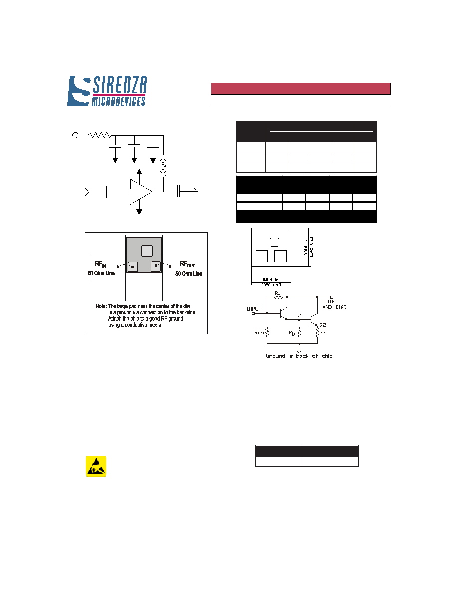
Typical Application Circuit
For recommended handling, die attach, and bonding methods, see the following application note at
www.sirenza.com.
AN-041 (PDF) Handling of Unpackaged Die
e
c
n
e
r
e
f
e
R
r
o
t
a
n
g
i
s
e
D
)
z
h
M
(
y
c
n
e
u
q
e
r
F
0
0
5
0
5
8
0
5
9
1
0
0
4
2
0
0
5
3
C
B
F
p
0
2
2
F
p
0
0
1
F
p
8
6
F
p
6
5
F
p
9
3
C
D
F
p
0
0
1
F
p
8
6
F
p
2
2
F
p
2
2
F
p
5
1
L
C
H
n
8
6
H
n
3
3
H
n
2
2
H
n
8
1
H
n
5
1
RF in
RF out
1 uF
C
B
C
B
C
D
R
BIAS
L
C
1
2
3
4
1000
pF
SNA-100
Suggested Bonding Arrangement
(above configuration used for S-parameter data)
Part Number Ordering Information
r
e
b
m
u
N
t
r
a
P
k
c
a
P
l
e
G
S
0
0
1
-
A
N
S
k
c
a
p
r
e
p
.
s
c
p
0
0
1
Caution: ESD sensitive
Appropriate precautions in handling, packaging
and testing devices must be observed.
Die are shipped per Sirenza application note
AN-039 Visual Criteria For Unpackaged Die
Application Circuit Element Values
Simplified Schematic of MMIC
Supply Voltage (V
S
)
6V
8V
10V
12V
R
BIAS
60
110
160
210
Note: R
BIAS
provides DC bias stability over temperature.
Recommended Bias Resistor Values for I
D
= 40mA
R
BIAS
= (V
S
- V
D
) / I
D
RFIN
RFOUT
GND
VIA
Die Thickness - 0.004 [0.1]
Dimensions - inches [mm]