ST
Sitronix
ST23L1610
16-Mbit (2M x 8 / 1M x16 ) Mask ROM
Ver 1.0
1
/
6 2002-Sep-13
F
F
E
E
A
A
T
T
U
U
R
R
E
E
S
S
Bit organization
- 2M x 8 (byte mode)
- 1M x 16 (word mode)
Fast access time
- 150ns (max.) @ 2.6V ~ 3.6V
Current
- Operating: 25mA
- Standby: 15uA
Supply voltage
- 2.6V ~ 3.6V
B
B
L
L
O
O
C
C
K
K
D
D
I
I
A
A
G
G
R
R
A
A
M
M
G
G
E
E
N
N
E
E
R
R
A
A
L
L
D
D
E
E
S
S
C
C
R
R
I
I
P
P
T
T
I
I
O
O
N
N
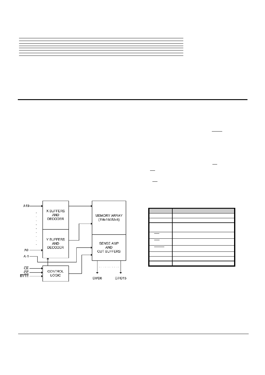
The ST23L1610 is a wide range operation, 16M-bit, Read
Only Memory. It is organized as 2M x 8 bits (byte mode) or
as 1M x 16 bit (word mode) depending on BYTE
(pin)
voltage level. ST23L1610 has a static standby mode, and
has an access time of 150 ns. It is designed to be
compatible with all microprocessors and similar
applications in which high performance, large bit storage
and simple interfacing are important design considerations.
ST23L1610 offers automatic power-down, with
power-down controlled by the chip enable ( CE
) input.
When CE
is not selected, the device automatically
powers down and remains in a low-power standby mode as
long as CE
stays in the unselected mode.
P
P
I
I
N
N
D
D
E
E
S
S
C
C
R
R
I
I
P
P
T
T
I
I
O
O
N
N
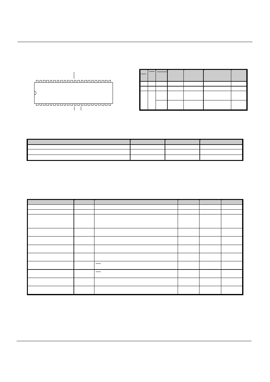
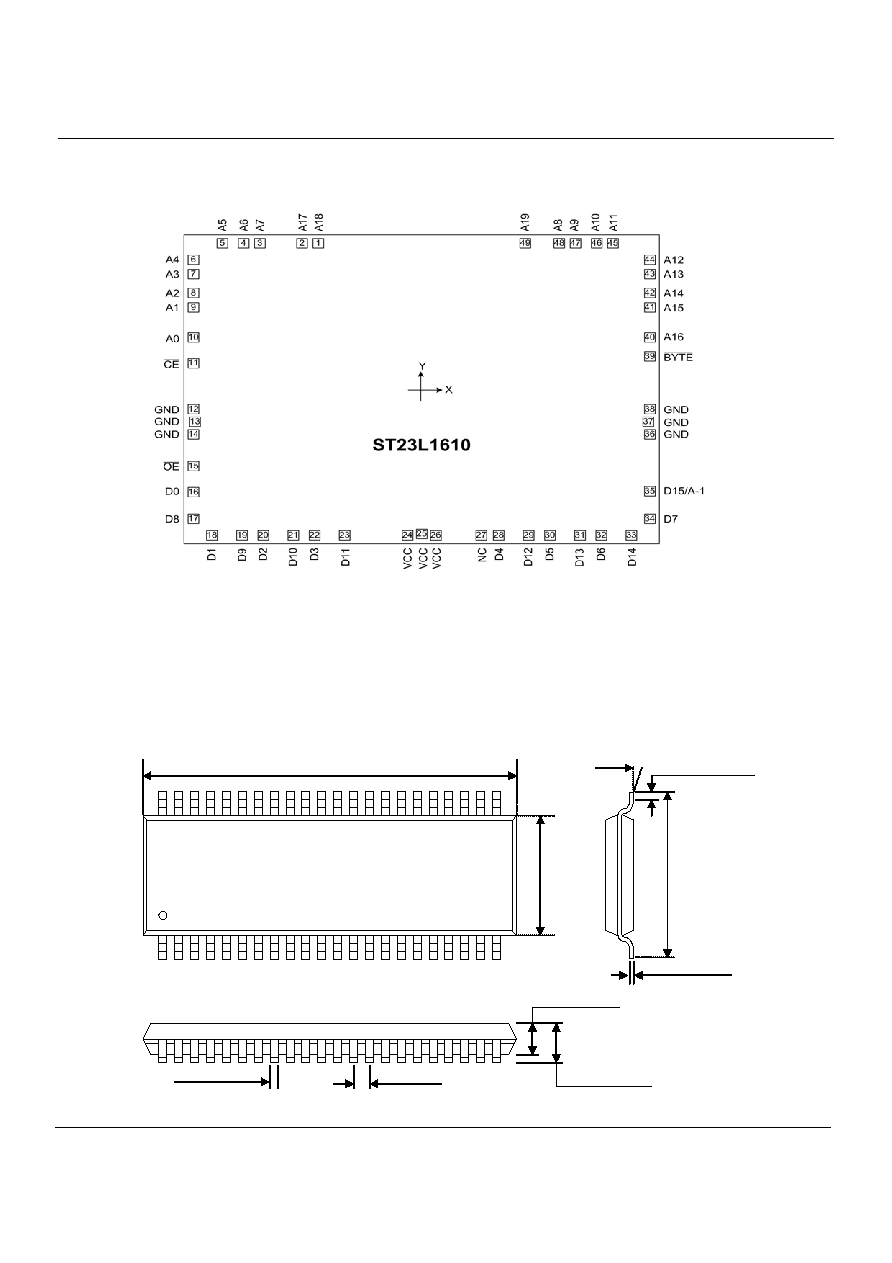
Symbol
Pin Function
A0~A19 Address
Inputs
D0~D14 Data
Outputs
D15/A-1
D15 (Word Mode) / LSB Address
(Byte Mode)
CE
Chip Enable Input
OE
Output Enable Input
BYTE
Word/Byte Mode Selection
VCC
Power Supply Pin
GND Ground
Pin
NC No
Connection
Sitronix ST23L1610
Ver 1.0
2/6
2002-Sep-13
P
P
I
I
N
N
C
C
O
O
N
N
F
F
I
I
G
G
U
U
R
R
A
A
T
T
I
I
O
O
N
N
2
3
4
5
6
7
8
9
10
11
12
13
14
1
15
16
17
18
19
NC
A1
8
A1
7
A7
A6
A5
A4
A3
A2
A1
A0
CE
GN
D
OE
D0
D8
D1 D9
D2
20
D10
NC
A1
9
A8
A9
A1
0
A1
1
A1
2
A1
3
A1
4
A1
5
A1
6
BY
T
E
GN
D
D15
/
A
-
1
D7
D14
D6
D13
D5
D12
21
D3
D4
22
D11
VC
C
33
32
31
30
29
28
27
26
25
24
23
43
42
41
40
39
38
37
36
35
34
44
44SOP
M
M
O
O
D
D
E
E
S
S
E
E
L
L
E
E
C
C
T
T
I
I
O
O
N
N
CE
OE
BYTE
D15/A-1 Mode
Data
Power
H X X
X Standby
High-Z Standby
L H X
X Operating High-Z
Active
H Output
Operation
(Word)
D0~D15: Dout Active
L L
L Input
Operation
(Byte)
D0~D7: Dout
D8~D14: Hi-Z
Active
A
A
B
B
S
S
O
O
L
L
U
U
T
T
E
E
M
M
A
A
X
X
I
I
M
M
U
U
M
M
R
R
A
A
T
T
I
I
N
N
G
G
S
S
Item
Symbol
Ratings
Unit
Voltage on Any Pin Relative to GND
V
IN
-0.3 to 4.3
V
Ambient Operating Temperature
T
OPR
0 to 70
Storage Temperature
T
STG
-65 to 125
NOTE: Minimum DC voltage on input or I/O pins is -0.5V. During Voltage transitions, inputs may undershoot GND to -1.3V for periods of
up to 20ns. Maximum DC voltage on input or I/O pins is VCC+0.5V. During voltage transitions, input may overshoot VCC to
VCC+2.0V for periods of up to 20ns.
D
D
C
C
C
C
H
H
A
A
R
R
A
A
C
C
T
T
E
E
R
R
I
I
S
S
I
I
C
C
S
S
(
(
T
T
A
A
=
=
0
0
�
�
C
C
~
~
7
7
0
0
�
�
C
C
,
,
V
V
C
C
C
C
=
=
2
2
.
.
6
6
V
V
~
~
3
3
.
.
6
6
V
V
)
)
Item
Symbol
Conditions
Min.
Max.
Unit
Output High Voltage
VOH
IOH=-400uA 2.3V
-
V
Output Low Voltage
VOL
IOL=1.6mA -
0.4V
V
Input High Voltage
VIH
MAX. number:
VCC+0.3V is under normal operation mode.
VCC+0.7V is under non-operating mode
2.1V VCC+0.3 V
Input Low Voltage
VIL
-0.3V
0.2xVCC
V
Input Leakage Current
ILI
0V, VCC
-
5
uA
Output Leakage Current
ILO
0V, VCC
-
5
uA
Operating Current
ICC1
tRC=120ns, all output open
-
25
mA
Standby Current (TTL)
ISB1
CE =VIH
- 0.5
mA
Standby Current (CMOS)
ISB2
CE >VCC-0.2V
- 15 uA
Input Capacitance
CIN
Ta=25, f=1MHz
- 10 pF
Output Capacitance
COUT
Ta=25, f=1MHz
- 10 pF
Sitronix ST23L1610
Ver 1.0
3/6
2002-Sep-13
A
A
C
C
C
C
H
H
A
A
R
R
A
A
C
C
T
T
E
E
R
R
I
I
S
S
I
I
C
C
S
S
(
(
T
T
A
A
=
=
0
0
�
�
C
C
~
~
7
7
0
0
�
�
C
C
,
,
V
V
C
C
C
C
=
=
2
2
.
.
6
6
V
V
~
~
3
3
.
.
6
6
V
V
)
)
Item
Symbol
Min.
Max.
Unit
Read Cycle Time
tRC
150 - nS
Address Access Time
tAA
- 150 nS
Chip Enable Access Time
tACE
- 150 nS
Output Enable Time
tOE
- 70 nS
Output Hold After Address
tOH
0 - nS
Output High-Z Delay
tHZ
- 20 nS
Note: Output high-impedance delay (tHZ) is measured from
OE
or
CE
going high, and this parameter guaranteed by design over the
full voltage and temperature operating range � not tested.
A
A
C
C
T
T
E
E
S
S
T
T
C
C
O
O
N
N
D
D
I
I
T
T
I
I
O
O
N
N
S
S
Input Pulse Levels
0.4V~2.4V
Input Rise and Fall Times
10nS
Input Timing Level
1.4V
Output Timing Level
1.4V
Output Load
See Figure
DOUT
C<100pF
IOL (load)= 1.6 mA
IOH (load)= -0.4 mA
Note:
No output loading is present in tester load board.
Active loading is used and under software programming control.
Output loading capacitance includes load board's and all stray capacitance.
T
T
I
I
M
M
I
I
N
N
G
G
D
D
I
I
A
A
G
G
R
R
A
A
M
M
RANDOM READ
Sitronix ST23L1610
Ver 1.0
4/6
2002-Sep-13
D
D
E
E
V
V
I
I
C
C
E
E
I
I
N
N
F
F
O
O
R
R
M
M
A
A
T
T
I
I
O
O
N
N
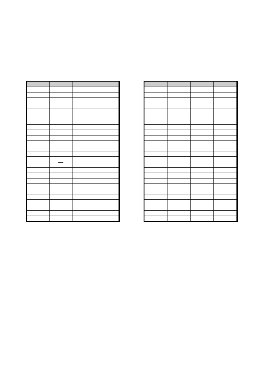
1. Pad size: 90um x 90 um
2. Substrate:
GND
3. Chip size: 6050 um x 4430 um
PAD No.
Symbol
X
Y
1 A18
-1315.0
2094.0
2 A17
-1522.0
2094.0
3 A7
-2059.0
2094.0
4 A6
-2265.0
2094.0
5 A5
-2536.0
2094.0
6 A4
-2904.0
1858.0
7 A3
-2904.0
1652.0
8 A2
-2904.0
1381.0
9 A1
-2904.0
1174.0
10 A0
-2904.0
743.0
11
CE -2904.0 372.0
12 GND
-2904.0
-285.0
13 GND
-2884.0
-465.0
14 GND
-2904.0
-645.0
15
OE -2904.0
-1101.0
16 D0
-2904.0
-1474.0
17 D8
-2904.0
-1857.0
18 D1
-2669.0
-2094.0
19 D9
-2286.0
-2094.0
20 D2
-2015.0
-2094.0
21 D10
-1633.0
-2094.0
22 D3
-1362.0
-2094.0
23 D11 -980.0
-2094.0
24 VCC -179.0
-2094.0
25 VCC
1.0
-2074.0
PAD No.
Symbol
X
Y
26 VCC 181.0
-2094.0
27 NC 759.0
-2094.0
28 D4 980.0
-2094.0
29 D12 1362.0
-2094.0
30 D5 1633.0
-2094.0
31 D13 2016.0
-2094.0
32 D6 2286.0
-2094.0
33 D14 2669.0
-2094.0
34 D7 2904.0
-1857.0
35 D15/A-1 2904.0
-1462.0
36 GND 2904.0
-645.0
37 GND 2884.0
-465.0
38 GND 2904.0
-285.0
39
BYTE 2904.0 472.0
40 A16 2904.0
743.0
41 A15 2904.0
1174.0
42 A14 2904.0
1381.0
43 A13 2904.0
1652.0
44 A12 2904.0
1858.0
45 A11 2435.0
2094.0
46 A10 2228.0
2094.0
47 A9 1958.0
2094.0
48 A8 1751.0
2094.0
49 A19 1319.0
2094.0
Sitronix ST23L1610
Ver 1.0
5/6
2002-Sep-13
P
P
A
A
D
D
D
D
I
I
A
A
G
G
R
R
A
A
M
M
P
P
A
A
C
C
K
K
A
A
G
G
E
E
I
I
N
N
F
F
O
O
R
R
M
M
A
A
T
T
I
I
O
O
N
N
44SOP (500mil)
0.
49
2
(
1
2.
5
0
)
M
I
N
0.
50
0
(
1
2.
7
0
)
M
A
X
0.009(0.229)MIN
0.0125(0.318)MAX
0.
61
2
(
1
5.
5
4
)
M
I
N
0.
65
1
(
1
6.
5
4
)
M
A
X
0.020(0.5)MIN
0.043(1.10)MAX
0~8
1.114(28.30)MIN
1.130(28.70)MAX
0.015(0.405)MIN
0.0165(0.420)MAX
0.05(1.270)
TYP
0.109(2.769)MIN
0.126(3.200)MAX
0.098(2.489)MIN
0.122(3.099)MAX
Unit:inches(mm)
#1
#44