ST
ST3001
PRELIMINARY
Speech Decoder
Notice: This is not a final specification. Some parameters are subject to change.
Ver 0.2b
1
/
10 2003-Sep-19
1
1
.
.
F
F
E
E
A
A
T
T
U
U
R
R
E
E
S
S
!
DSP based audio processor with 40MHz clock
!
One PLL to generate high system frequency from a
3.58MHz crystal/resonator
!
Operation voltage
� Core logic/analog blocks: 2.25V~2.7V
� I/O pads: 2.4V~3.6V
!
Low voltage regulator for core logic
!
Low Voltage Reset (LVR)
!
Low power down current: 2uA
!
Decompression data rate
� 32.02Kbps ADPCM / 8.33K/ 6.66K/ 6.02 K/ 4.82K/
2.42Kbps
!
One 10-bit Current DAC
� Class-AB DAC driver
� Directly drive external 8-ohm's speaker or headset
� Support ramp up, ramp down, and volume control
!
MCU interfaces
� Serial/parallel interface supported
� 8-byte data buffer for burst access
2
2
.
.
G
G
E
E
N
N
E
E
R
R
A
A
L
L
D
D
E
E
S
S
C
C
R
R
I
I
P
P
T
T
I
I
O
O
N
N
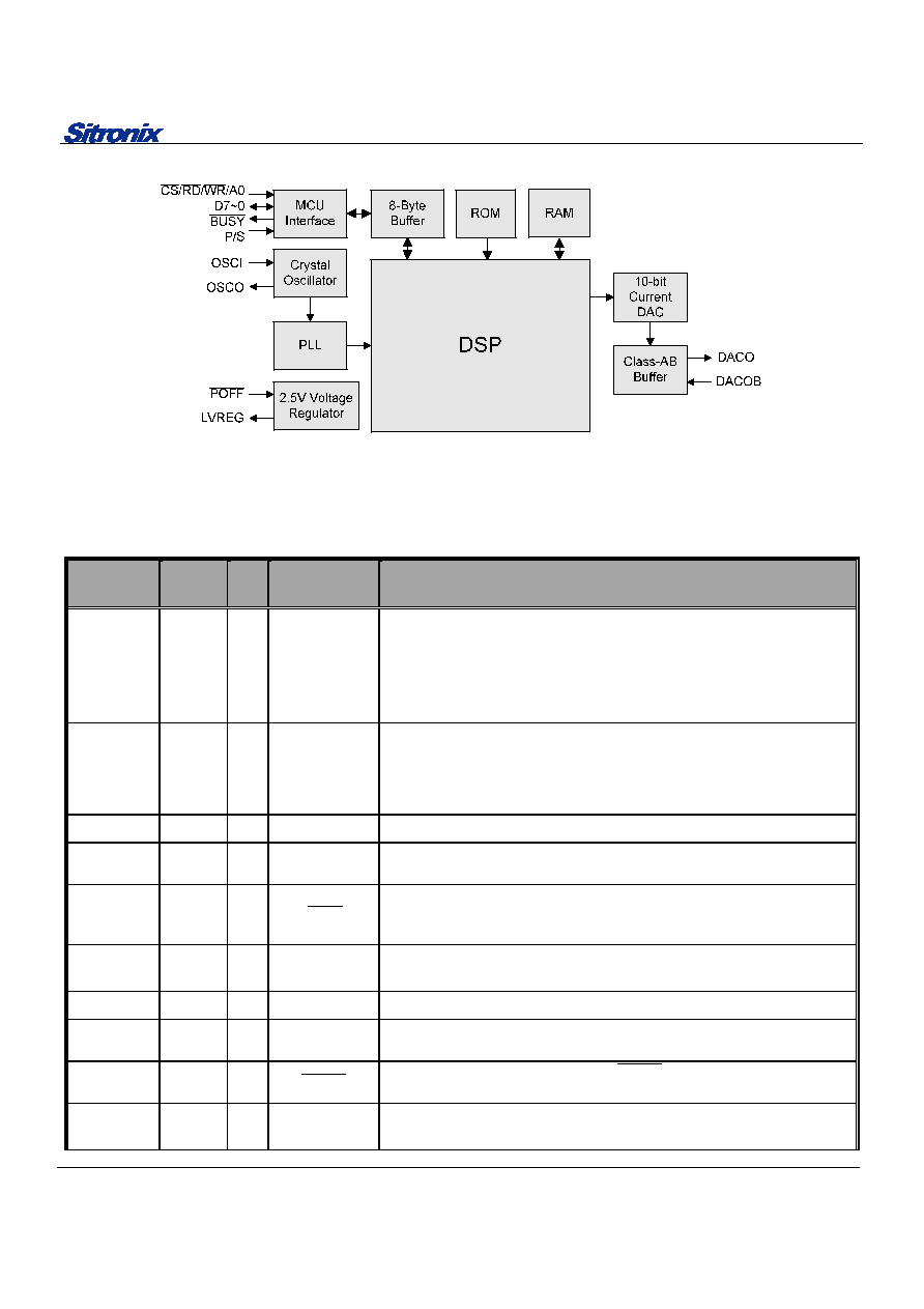
The ST3001 is a highly integrated and cost-effective DSP
based audio processor for various consumer applications. It
consists of one powerful DSP for advanced voice decoder
algorithms for natural speech with less memory. The
decompression data rate can be 32.02Kbps, 8.33Kbps,
6.66Kbps, 6.02Kbps, 4.82Kbps and 2.42Kbps.
One PLL is equipped to generate high system clock from a
low-lost 3.58MHz crystal/resonator or external clock input. For
voice playback, one 10-bit current DAC with a class-AB output
buffer provides the output signal conversion and the ability of
directly driving of an external 8-ohm's speaker or a headset.
Besides, functions such as frequency sliding, playback speed
control, ramp up/down and volume control, etc. are also
designed for better performance.
The ST3001 has a voltage regulator that generates a 2.5V
voltage for most logic and analog blocks with only few
components. One power-down mode is also supported for
reducing the power consumption. When power control pin,
POFF
, is low, this voltage regulator will be off, and only few
current about 2uA is needed at this time.
There are two kinds of interfaces, parallel and serial, for
various connection to different MCUs. Besides, one data buffer
of 8-byte length makes communication easier and more
efficient.
ST3001
Ver 0.2b
2/10
2003-Sep-19
FIGURE 2-1 ST3001 Block Diagram
3
3
.
.
S
S
I
I
G
G
N
N
A
A
L
L
D
D
E
E
S
S
C
C
R
R
I
I
P
P
T
T
I
I
O
O
N
N
S
S
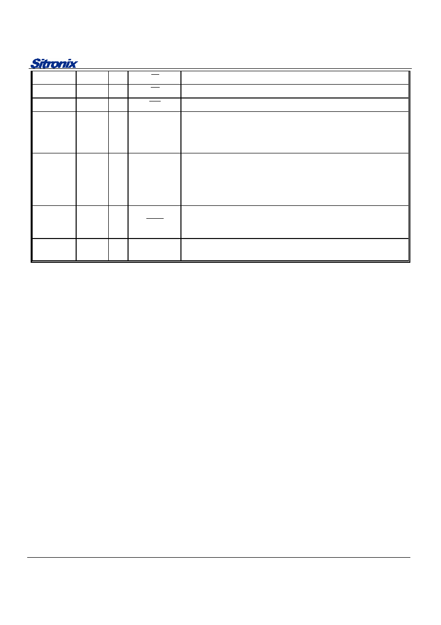
TABLE 3-1 Signal Function Description
Function
Group
Pad No. I/O
Designation
Description
Power
12,17,22
31,35,36
42,70
P
VCC, LVCC,
AVCC, BVCC
RVCC
VCC:
Power supply for I/O pads
RVCC:
Power supply for low voltage regulator
LVCC:
Power supply for core logic, connect to 2.5V
AVCC:
Power supply for analog circuit, connect to 2.5V
BVCC:
Power supply for bandgap reference, connect to 2.5V
Ground
1,7,13,
18,21,29
50,59
P
GND, LGND,
AGND, BGND
GND:
Ground for I/O pads
LGND:
Ground for core logic
AGND:
Ground for analog circuit
BGND:
Ground for bandgap reference
Voice output
19,20
O
DACO/DACOB
Outputs for current DAC
Regulator 32 O LVREG
Output for LVCC regulator control signal. Connect to the base terminal of the
external NPN transistor.
33
I
POFF
When this pin is low, low voltage regulator will be off, and ST3001 enters the
power down mode. After inputted high and wakes ST3001 up, there must
follows a reset pulse to recover the normal operation.
System
control
15,16 I/O OSCI,
OSCO Crystal oscillator input/output
2
I
TEST
Test pin. Leave it open when normal operation
30
I
BREF
Input for bandgap reference voltage. Connect one resistor between this pin
and GND.
28
I
RESET
Active low system reset signal input. RESET should be pulled up to 2.5V
with a resistor of 47k and connects to an open-drain output of the MCU.
MCU
interface
64 I
P/S
"L": select serial interface
"H": select parallel interface
ST3001
Ver 0.2b
3/10
2003-Sep-19
65
I
CS
Active low chip select input
66
I RD
Active low read signal input
67
I WR
Active low write signal input
63
I A0
Connect to least significant bit of standard MPU address bus, and it
determines whether the data register or control register is selected.
"H": select data register.
"L": select control register.
54~58
60~62
I/O
D7/SCL
D6/SDI
D5/SDO
D4~D0
Parallel mode (P/S = "H"):
D[7:0]:
8-bit bi-directional data bus to connect to standard MCUs.
Serial mode (P/S = "L"):
D7/SCL:
serial clock input
D6/SDI:
serial data input
D5/SDO:
serial data output
68 O BUSY
Buffer read/write interrupt request signal output.
"L" : Buffer is not empty or system is busy
"H" : Buffer is empty
No
connection
NC
ST3001
Ver 0.2b
4/10
2003-Sep-19
4
4
.
.
P
P
A
A
D
D
D
D
I
I
A
A
G
G
R
R
A
A
M
M
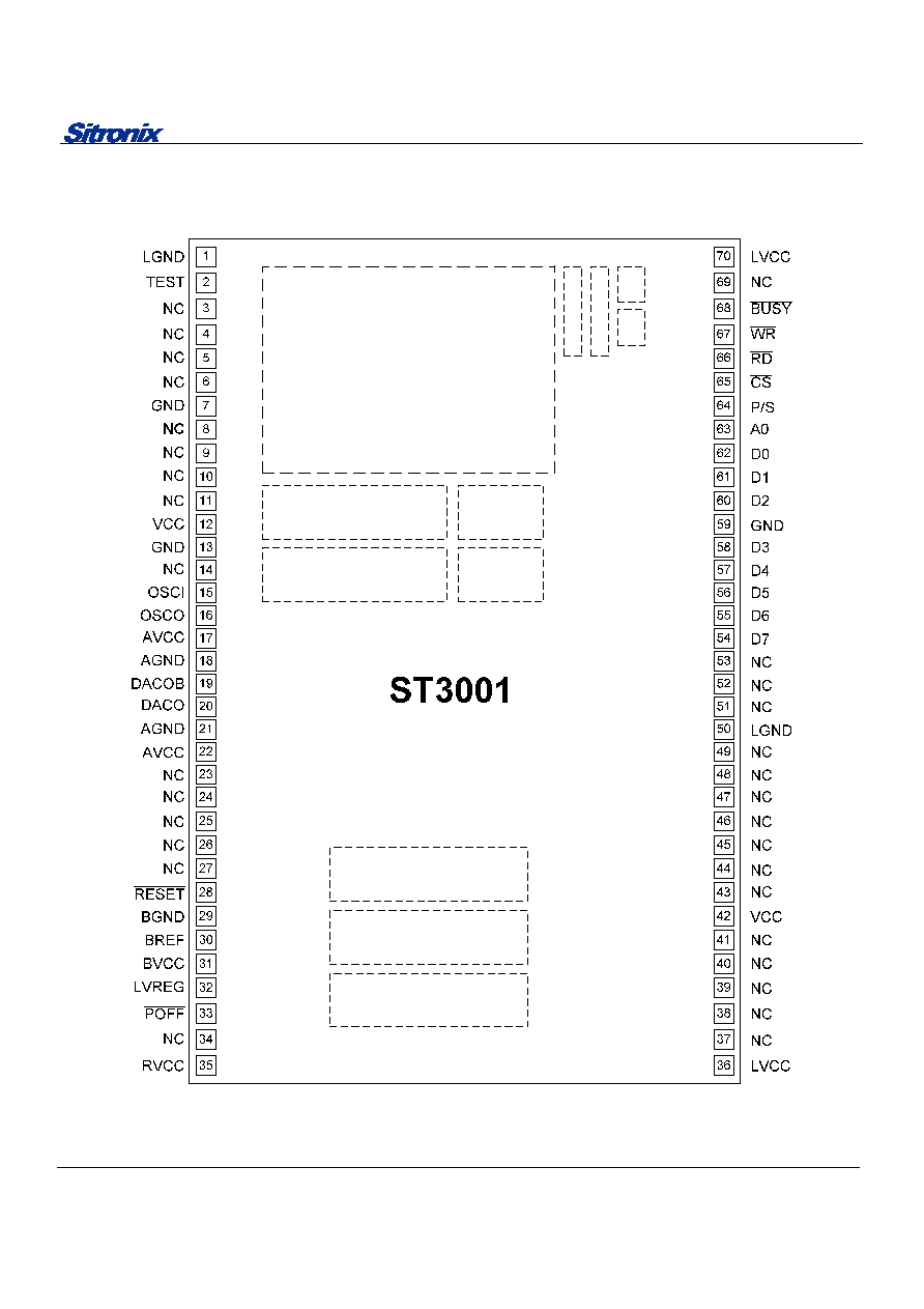
ST3001
Ver 0.2b
5/10
2003-Sep-19
5
5
.
.
D
D
E
E
V
V
I
I
C
C
E
E
I
I
N
N
F
F
O
O
R
R
M
M
A
A
T
T
I
I
O
O
N
N
1.
Pad size: 90um x 90um
2. Substrate:
GND
3.
Chip size: 2483um x 3835um
PAD No.
Symbol
X
Y
PAD No.
Symbol
X
Y
1
LGND
-1193.9
1870
36
LVCC
1193.9
-1870
2
TEST
-1193.9
1750
37
NC
1193.9
-1750
3
NC
-1193.9
1630
38
NC
1193.9
-1630
4
NC
-1193.9
1510
39
NC
1193.9
-1510
5
NC
-1193.9
1400
40
NC
1193.9
-1400
6
NC
-1193.9
1290
41
NC
1193.9
-1290
7
GND
-1193.9
1180
42
VCC
1193.9
-1180
8
NC
-1193.9
1070
43
NC
1193.9
-1070
9
NC
-1193.9
960
44
NC
1193.9
-960
10
NC
-1193.9
850
45
NC
1193.9
-850
11
NC
-1193.9
740
46
NC
1193.9
-740
12
VCC
-1193.9
630
47
NC
1193.9
-630
13
GND
-1193.9
525
48
NC
1193.9
-525
14
NC
-1193.9
420
49
NC
1193.9
-420
15
OSCI
-1193.9
315
50
LGND
1193.9
-315
16
OSCO
-1193.9
210
51
NC
1193.9
-210
17
AVCC
-1193.9
105
52
NC
1193.9
-105
18
AGND
-1193.9
0
53
NC
1193.9
0
19
DACOB
-1193.9
-105
54
D7/SCL
1193.9
105
20
DACO
-1193.9
-210
55
D6/SDI
1193.9
210
21
AGND
-1193.9
-315
56
D5/SDO
1193.9
315
22
AVCC
-1193.9
-420
57
D4
1193.9
420
23
NC
-1193.9
-525
58
D3
1193.9
525
24
NC
-1193.9
-630
59
GND
1193.9
630
25
NC
-1193.9
-740
60
D2
1193.9
740
26
NC
-1193.9
-850
61
D1
1193.9
850
27
NC
-1193.9
-960
62
D0
1193.9
960
28
RESET
-1193.9
-1070
63
A0
1193.9
1070
29
BGND
-1193.9
-1180
64
P/S
1193.9
1180
30
BREF
-1193.9
-1290
65
CS
1193.9
1290
31
BVCC
-1193.9
-1400
66
RD
1193.9
1400
32
LVREG
-1193.9
-1510
67
WR
1193.9
1510
33
POFF
-1193.9
-1630
68
BUSY
1193.9
1630
34
NC
-1193.9
-1750
69
NC
1193.9
1750
35
RVCC
-1193.9
-1870
70
LVCC
1193.9
1870
ST3001
Ver 0.2b
6/10
2003-Sep-19
6
6
.
.
E
E
L
L
E
E
C
C
T
T
R
R
I
I
C
C
A
A
L
L
C
C
H
H
A
A
R
R
A
A
C
C
T
T
E
E
R
R
I
I
S
S
T
T
I
I
C
C
S
S
6.1 Absolute Maximum Rations
DC Supply Voltage: VCC/RVCC ------------ -0.3V to +4.5V
LVCC/AVCC/BVCC - -0.3V to +3.0V
Operating Ambient Temperature --------- -10
�
C to +60
�
C
Storage Temperature ------------------------ -10
�
C to +125
�
C
6.2 DC Electrical Characteristics
Standard operation conditions: VCC
= 3.0V, GND = 0V, T
A
= 25
�
C, unless otherwise specified
Parameter
Symbol
Min.
Typ.
Max.
Unit
Condition
Operating Voltage
VCC
2.4
3.6
V
Operating
Voltage
LVCC
2.25 2.5 2.75
V
Operating
Voltage
AVCC
2.25 2.5 2.75
V
Operating
Voltage
BVCC
2.25 2.5 2.75
V
Operating Voltage
RVCC
2.4
3.6
V
Operating Current
I
OP
1
41
mA
Without
playing
speech
Operating Current
I
OP
2
100
mA
With
playing
speech
Power Down Current
I
PD
2 5
�
A
Sleep Current
I
SL
230
�
A
Output low voltage
V
OL
0.4
V
I
OL
= 4mA
Output high voltage
V
OH
2.4
V
I
OH
= -2 ~ -8mA
Input Low Voltage
V
IL
0.8
V
LVTTL
Input High Voltage
V
IH
2.0
V
LVTTL
Pull-up resistor
R
PU
40 75 190
K
Pull-down resistor
R
PD
40 75 190
K
Input Leakage Current
I
IN
<1
�A
V
IN
= VCC or 0
Low Voltage Reset Level
V
LVR
1.9 2.0 2.1
DAC Full Scale Output Voltage
(driven by internal post amp)
V
PP
1 3.6
V
DAC Full Scale Output Current
(To external BJT)
I
PP
0.762 3.84
mA
*Note:
Stresses above those listed under "Absolute Maximum
Ratings" may cause permanent damage to the device. All the
ranges are stress ratings only. Functional operation of this
device at these or any other conditions above those indicated
in the operational sections of this specification is not implied or
intended. Exposed to the absolute maximum rating conditions
for extended periods may affect device reliability.
ST3001
Ver 0.2b
7/10
2003-Sep-19
6.3 AC Electrical Characteristics
SCL
SDI
SDO
t
CSS
t
DS
t
DH
t
DD
t
DS
t
CYC
CS_
Serial Interface
FIGURE 6-1 Serial Interface Timing Diagram
A0
CS_
WR_
D[7:0]
RD_
t
AW
t
CCLR
t
DS
t
DH
t
AH
t
AW
t
AH
t
ACC
t
OH
t
CCLW
t
CCHW
t
CCHR
Parallel Interface
FIGURE 6-2 Parallel Interface Timing Diagram
TABLE 6-1 Timing parameters for FIGURE 6-1
Standard operation conditions: VCC
= 3.0V, GND = 0V, T
A
= 25
�
C
Rating
Symbol
Characteristic
Min.
Typ.
Max.
Unit
t
CSS
CS
low
to
1
st
SCL rising
100
nS
t
CYC
SCL
cycle
time
200
nS
t
DS
Data valid prior SCL falling
0
nS
t
DH
Data Hold time after SCL rising
10
nS
t
DD
SDO output delay from SCL falling
10
nS
ST3001
Ver 0.2b
8/10
2003-Sep-19
TABLE 6-2 Timing parameters for FIGURE 6-2
Standard operation conditions: VCC
= 3.0V, GND = 0V, T
A
= 25
�
C
Rating
Symbol
Characteristic
Min.
Typ.
Max.
Unit
t
AH
Address
hold
time
0
nS
t
AW
Address
setup
time
0
nS
t
CYC
System cycle time
240
nS
t
CCLW
Write pulse width
80
nS
t
CCHW
Enable H write width
80
nS
t
CCLR
Read pulse width
140
nS
t
CCHR
Enable H read width
80
nS
t
DS
Write
data
setup
time
40
nS
t
DH
Write data hold time
0
nS
t
ACC
Read access time
70
nS
t
OH
Read data disable time
5
50
nS
ST3001
Ver 0.2b
9/10
2003-Sep-19
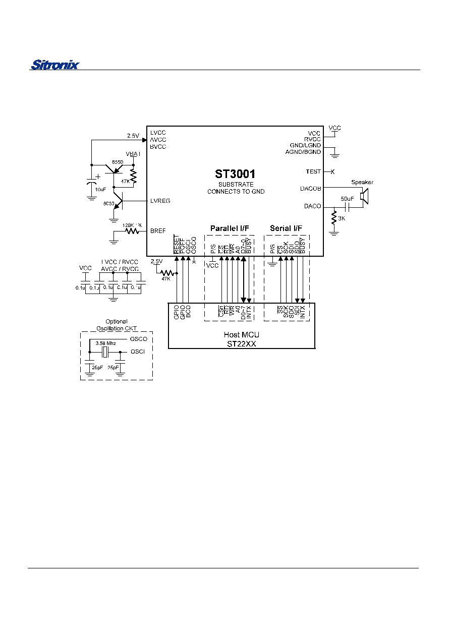
7
7
.
.
A
A
P
P
P
P
L
L
I
I
C
C
A
A
T
T
I
I
O
O
N
N
C
C
I
I
R
R
C
C
U
U
I
I
T
T

ST3001
Ver 0.2b
10/10
2003-Sep-19
8
8
.
.
R
R
E
E
V
V
I
I
S
S
I
I
O
O
N
N
S
S
REVISION DESCRIPTION
PAGE
DATE
0.2b
!
Change pin function and name of
WAKE
to NC
!
Modify description of POFF in section 3
!
Modify application circuit in section 7
2
9
2003/9/19
0.1 First
release
2003/7/13