Skyworks Solutions, Inc. [978] 241-7000
∑ Fax [978] 241-7906 ∑ Email sales@skyworksinc.com ∑ www.skyworksinc.com
1
Specifications subject to change without notice. 12/02A
25≠32 GHz GaAs MMIC
Low Noise Pre-Amplifier
Features
Single Bias Supply Operation (3.5 V or 5 V)
2.5 dB Typical Noise Figure at 26 GHz
28 dB Typical Small Signal Gain
100% On-Wafer RF, DC and Noise
Figure Testing
100% Visual Inspection to MIL-STD-883
MT 2010
Ideal for Ka Band SatCom and Point to
Multi-Point Applications
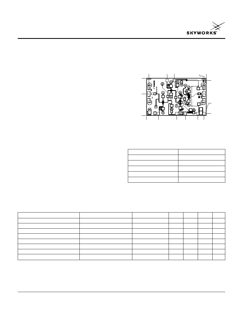
Chip Outline
AA028N2-00
Description
Skyworks' four-stage, reactively-matched GaAs MMIC
amplifier has a typical small signal gain of 28 dB with a
typical noise figure of 2.5 dB with P
1 dB
> 14 dBm at
26 GHz. The device is ideal for Ka band SatCom and point
to multi-point applications. The FETs employ surface
passivation to ensure a rugged, reliable part with
through-substrate via holes and gold-based backside
metallization to facilitate a conductive epoxy or solder die
attach process. The RF interface has been designed for
high volume automatic bonding assembly, allowing for
(2) 1.0 mil Au wire. All chips are screened for
S-parameters, output power and noise figure prior to
shipment for guaranteed performance.
Parameter
Condition
Symbol
Min.
Typ.
3
Max.
Unit
Drain Current
I
DS
245
275
mA
Small Signal Gain
F = 25≠31 GHz
G
27
28
dB
Noise Figure
F = 26 GHz
NF
2.5
3.0
dB
Input Return Loss
F = 25≠31 GHz
RL
I
-9
-6
dB
Output Return Loss
F = 25≠31 GHz
RL
O
-12
-6
dB
Output Power at 1 dB Gain Compression
1
F = 26 GHz
P
1 dB
14
dBm
Two-Tone Output Third-Order Intercept1
F = 28 GHz
OIP3
21
dBm
Thermal Resistance
2
JC
TBD
∞C/W
Electrical Specifications at 25∞C (V
DS
= 3.5 V or 5 V)
4
0.088
(2.24 mm)
0.004
(0.10 mm)
SQ TYP.
0.000
0.018
(0.46 mm)
0.046
(1.17 mm)
0.059
(1.50 mm)
0.078
(1.98 mm)
0.091
(2.31 mm)
0.000
0.033
(0.84 mm)
0.057
(1.45 mm)
0.003
(0.08 mm)
0.054
(1.37 mm)
0.003
(0.08 mm)
0.031
(0.79 mm)
0.043
(1.09 mm)
0.088
(2.24 mm)
Characteristic
Value
Operating Temperature (T
C
)
-55∞C to +90∞C
Storage Temperature (T
ST
)
-65∞C to +150∞C
Bias Voltage (V
D
)
6 V
DC
Power In (P
IN
)
10 dBm
Junction Temperature (T
J
)
175∞C
Absolute Maximum Ratings
1. Not measured on a 100% basis.
2. Calculated value based on measurement of discrete FET.
3. Typical represents the median parameter value across the specified
frequency range for the median chip.
4. 3.5 V is applied to V
D1
pad, or 5 V is applied to V
D2
pad.
Preliminary

25≠32 GHz GaAs MMIC Low Noise Pre-Amplifier
AA028N2-00
2
Skyworks Solutions, Inc. [978] 241-7000
∑ Fax [978] 241-7906 ∑ Email sales@skyworksinc.com ∑ www.skyworksinc.com
Specifications subject to change without notice. 12/02A
Frequency (GHz)
Typical Small Signal Performance
S-Parameters (V
D1
= 3.5 V)
23 24 25 26 27 28 29 30 31 32 33 34
-60
-50
-40
-30
-20
-10
0
10
20
30
40
S-Parameters (dB)
S
11
S
12
S
22
S
21
Output P
1 dB
(dBm)
Frequency (GHz)
Output P
1 dB
vs. Frequency
(V
D1
= 3.5 V)
12
13
14
15
16
17
18
19
20
23 24 25 26 27 28 29 30 31 32 33 34
Frequency (GHz)
Two-Tone Output Third-Order
Intercept @ V
D2
= 5 V
OIP3 (dBm)
18
19
20
21
22
23
24
25
26
27
26
27
28
29
30
Noise Figure (dB)
Frequency (GHz)
Typical Noise Figure Performance
vs. Frequency (V
D1
= 3.5 V)
23 24 25 26 27 28 29 30 31 32 33 34
1.0
1.5
2.0
2.5
3.0
3.5
4.0
4.5
V
D2
(V)
Two-Tone Output Third-Order
Intercept @ 28 GHz
OIP3 (dBm)
19
20
21
22
23
24
4.0
4.5
5.0
5.5
6.0
Pin (dBm)
Output Power and Relative Third-Order
Intermodulation Products F = 28 GHz, V
D2
= 5 V
Pout (dBm)
-5
-4
-3
-2
-1
0
1
2
3
4
5
-27 -26
-25
-24
-23
-22
-21
-20
-19
-50
-48
-46
-44
-42
-40
-38
-36
-34
-32
-30
IM3 (dBc)
IM3
P
OUT
Typical Performance Data
25≠32 GHz GaAs MMIC Low Noise Pre-Amplifier
AA028N2-00
Skyworks Solutions, Inc. [978] 241-7000
∑ Fax [978] 241-7906 ∑ Email sales@skyworksinc.com ∑ www.skyworksinc.com
3
Specifications subject to change without notice. 12/02A
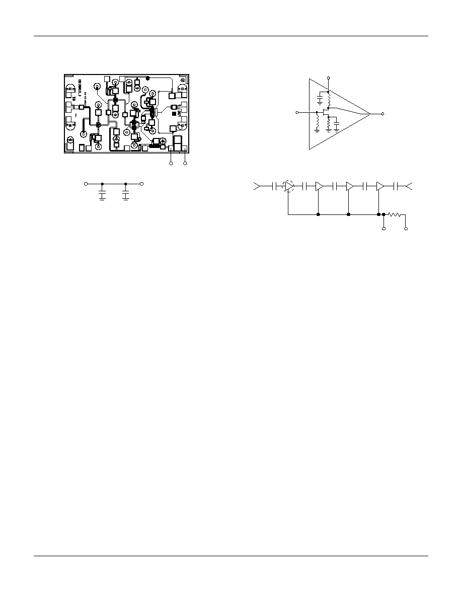
V
D
V
D2
V
D1
CONNECTED TO
V
D1
OR V
D2
RF IN
RF OUT
0.01
µF 50 pF
Bias Arrangement
RF IN
RF OUT
V
D1
V
D2
(Optional)
D
See
Detail A
Detail A
Circuit Schematic
For biasing on, adjust V
DS
from zero to the desired value (3.5 V = V
D1
or
5 V = V
D2
is recommended). For biasing off, reverse the biasing on procedure.
Recommended RF Bonding
Input: Two 1 mil wires
10 mils long.
Output: Two 1 mil wires 20 ± 5 mils long.