 | –≠–ª–µ–∫—Ç—Ä–æ–Ω–Ω—ã–π –∫–æ–º–ø–æ–Ω–µ–Ω—Ç: AP107-81 | –°–∫–∞—á–∞—Ç—å:  PDF PDF  ZIP ZIP |
Skyworks Solutions, Inc. [978] 241-7000
∑
Fax [978] 241-7906
∑
Email sales@skyworksinc.com
∑
www.skyworksinc.com
1
Specifications subject to change without notice. 3/99A
GaAs IC 1.9 GHz Power Amplifier
Features
PCS TDMA IS136
PCS CDMA IS95
Linear Power up to 31 dBm (PEP)
6 V Operation
Efficiency Greater Than 30%
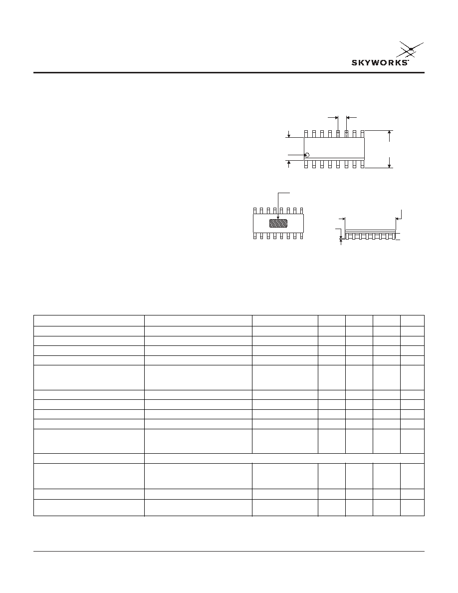
High Power 16 Lead SOIC Package
with Slug
SOIC-16 Slug
AP107-81
Description
The AP107-81 is a low cost IC power amplifier designed
for the 1.85≠1.91 GHz frequency band. It features 5
cell battery operation and operates with excellent
linearity and high efficiency. The amplifier is designed
to be stable over a temperature range of -30 to 100∞C and
over 3:1 VSWR loads.
Characteristic
Condition
Frequency
Min.
Typ.
Max.
Unit
Output Power (PEP)
P
IN
2 dBm (Avg.)
1.85≠1.91 GHz
31
dBm
Efficiency
P
OUT
(PEP) = 31 dBm
30
35
%
Gain (Small Signal)
P
IN
= -20 dBm
27
30
33
dB
Gain (Large Signal)
P
OUT
(PEP) = 31 dBm
25
28
31
dB
Noise in the Receive Band
P
OUT
(PEP) = 31 dBm
-100
-95
dBm
R
X
Band = 1930≠1990 MHz
R
X
Bandwidth = 30 kHz
Negative Bias Current
P
OUT
(PEP) = 31 dBm
6
8
mA
Input VSWR
P
IN
= -30 to +2 (Avg.)
2:1
IM3@ Rated P
OUT
P
OUT
= 31 dBm (PEP)
-26
dBc
IM5@ Rated P
OUT
P
OUT
= 31 dBm (PEP)
-35
dBc
Harmonic Power
P
OUT
= 31 dBm (PEP)
2fo
-30
dBc
3fo
-45
dBc
Modulation
Channel Spacing = 30 kHz, 832 Channels, Pi/4 QPSK
P
ADJ
30 kHz
-30
dBc
60 kHz
-50
dBc
90 kHz
-55
dBc
Input Impedance
50
Load Impedance
9-j5.4
(Measured at Pins 12 & 13)
Electrical Specifications at 25∞C
1,2
0.050 (1.27 mm) BSC
16
9
1
8
0.158 (4.00 mm)
0.150 (3.80 mm)
0.244 (6.20 mm)
0.228 (5.80 mm)
PIN
INDICATOR
16
9
1
8
0.394 (10.00 mm)
0.386 (9.80 mm)
0.65 (1.65 mm) MAX.
0.004
(0.010 mm)
MAX.
HEAT SLUG 0.066 X 0.140 REF
LOCATED ON CENTER-LINE
OF THE PACKAGE

2
Skyworks Solutions, Inc. [978] 241-7000
∑
Fax [978] 241-7906
∑
Email sales@skyworksinc.com
∑
www.skyworksinc.com
Specifications subject to change without notice. 3/99A
GaAs IC 1.9 GHz Power Amplifier
AP107-81
P
OUT
(dBm)
Gain (dB)
PAE (%)
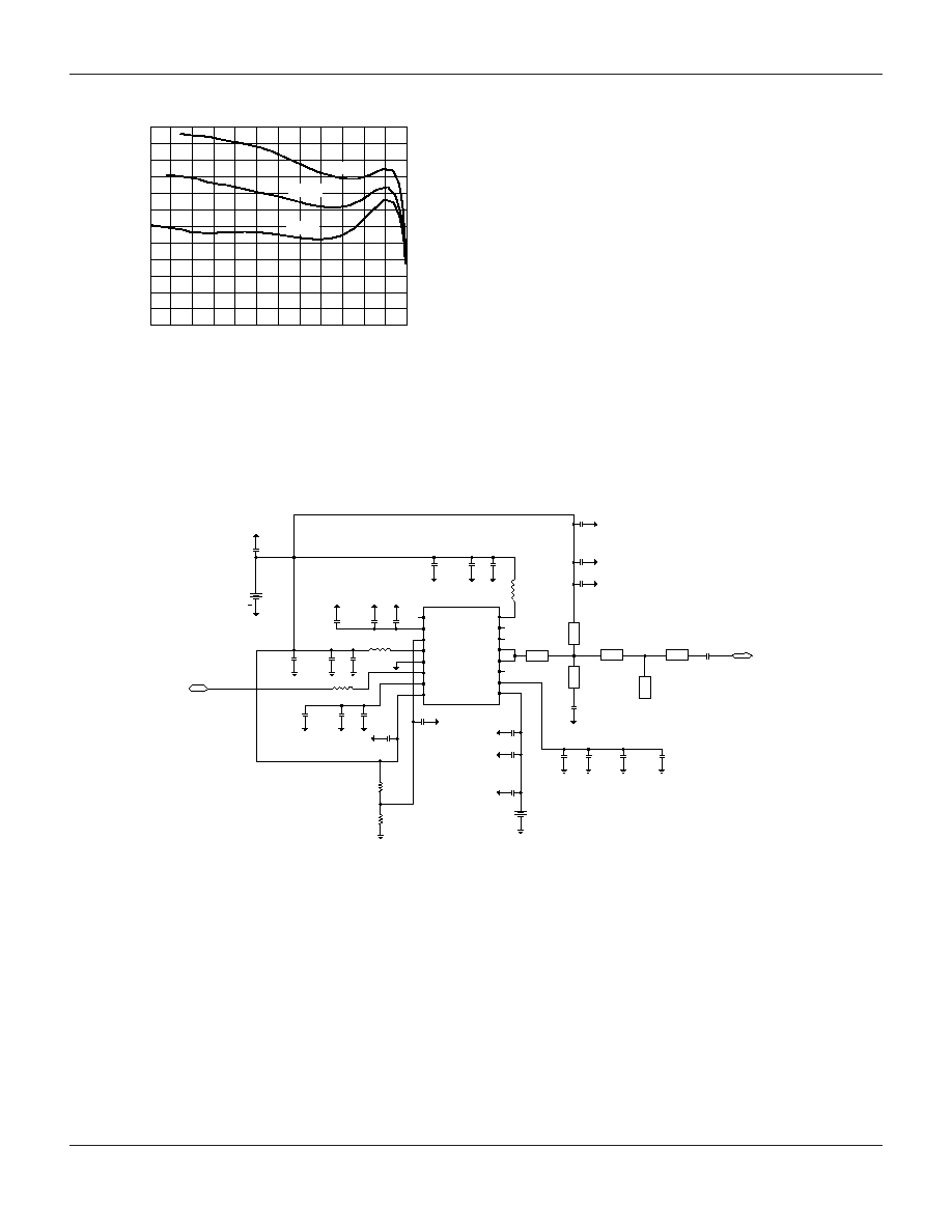
Figure 1. Gain, P.A.E. vs. Output Power
30
29
28
27
26
25
24
23
22
21
45
40
35
30
25
20
15
10
5
0
15 16 17 18 19 20 21 22 23 24 25 26 27 28 29 30
PAE
Gain
P
IN
(dBm)
P
OUT
(dBm)
34
32
30
28
26
24
22
20
18
16
14
12
10
8
-20-18-16-14 -12-10 -8 -6 -4 -2
0 2
4 6
8
6.5 V
5.8 V
5.0 V
Figure 3. P
OUT
vs. P
IN
Over Drain Voltage
P
OUT
(dBm)
Distortion (dBc)
Figure 2. Intermodulation
Distortion vs. Output Power
15 16 17 18 19 20 21 22 23 24 25 26 27 28 29 30
15
20
25
30
35
40
45
50
55
60
65
IM3
IM3
IM5
IM7
P
IN
(dBm)
P
OUT
(dBm)
Figure 4. P
OUT
vs. P
IN
Over Temperature
-20-18 -16-14-12-10 -8 -6 -4 -2
0 2
4 6 8
34
32
30
28
26
24
22
20
18
16
14
12
10
8
6
-30∞C
Room
+85∞C
P
OUT
(dBm)
Gain (dB)
Figure 5. Gain vs. P
OUT
Over Frequency
30.0
29.5
29.0
28.5
28.0
27.5
27.0
26.5
26.0
25.5
25.0
24.5
24.0
8 10 12 14 16 18 20 22 24 26 27 28 30
1.85 GHz
1.88 GHz
1.91 GHz
V
REF
(V)
ldq (mA)
Figure 6. Quiescent Current vs.
Reference Voltage
250
200
150
100
50
0
3.9 3.95
4.0 4.05
4.1 4.15
4.2 4.25
4.3
Idq
Typical Performance Data (1.85≠1.91 GHz)
1. Performance in Figures 1, 2, 3, 4 and 5 is with V
REF
set to 4.1 V through resistive voltage divider as shown in schematic.
2. Performance shown in Figures 1 and 2 is with a two-tone input signal at 1.88 GHz and 1.88001 GHz.
3. Performance in Figures 3, 4 and 7 is with a 1.88 GHz CW input signal.
4. For Figures 6 and 7, V
REF
was varied using a DC supply connected directly to the V
REF
pin.
Skyworks Solutions, Inc. [978] 241-7000
∑
Fax [978] 241-7906
∑
Email sales@skyworksinc.com
∑
www.skyworksinc.com
3
Specifications subject to change without notice. 3/99A
GaAs IC 1.9 GHz Power Amplifier
AP107-81
P
OUT
(dBm)
Gain (dB)
Figure 7. Gain vs. P
OUT
vs.
Reference Voltage
30.0
29.0
28.0
27.0
26.0
25.0
24.0
8 10 12 14 16 18 20 22 24 26 28 30 32
4.1 V
3.9 V
4.3 V
Output Matching Circuit
The output match for the AP107 is provided externally in
order to improve performance, reduce cost and add
flexibility. By making use of either ceramic surface mount
components or a distributed microstrip network, a much
lower loss match is achievable than could be obtained
using integrated elements on GaAs. This lower loss results
in better linearity and efficiency at rated output power for
the amplifier. Also, by keeping these elements external to
the GaAs IC, die size is smaller and the overall cost is thus
reduced. This off-chip approach also permits the flexibility
to tweak the amplifier for optimum performance at different
powers, and/or frequencies.
The board schematic demonstrates a distributed load
matching network on FR4 substrate, which presents the
optimum load match while also providing a path for
DC bias to the output stage.
Power Amplifier Typical Configuration
1
V
G2
V
REF
V
DD1
GND
RF In
V
G1
V
DBC
V
DD2
15
14
RF Out
RF
Out
11
V
G3
V
SS
Power Supply
Voltage
+
5.8 V
V
DD
10 µF
C21
C3
1000 pF
C6
1000 pF
C9
1000 pF
C15
1000 pF
C30
10 µF
C 20
1000 pF
C12
1000 pF
C28
1000 pF
C2
100 pF
C5
100 pF
C8
100 pF
C14
100 pF
C19
100 pF
C17
100 pF
C16
100 pF
C11
100 pF
C27
100 pF
C1
8.2 pF
C4
8.2 pF
C7
8.2 pF
C13
8.2 pF
Negative Supply Voltage
C18
8.2 pF
C10
8.2 pF
C26
8.2 pF
L3
12 nH
L1
1.8 nH
AP107-81
L2
3.3 nH
R1
R2
3.3k
8.2k
RF In
50
RF input
mline
W = 50 L = 50
mline
W = 50 L = 410
mline
W = 50 L = 130
mline
W = 50 L = 230
mline
W = 26 L = 70
C29
1.2 pF
mstub
W = 50 L = 100
C22
15 pF
RF Out
50
RF output
FR4 Substrate Parameters
Er = 4.5 H = 14 T = 0.7 Rho = 1.2
V
SS
+
-4 V
-
Bias Controller Circuit
An on-chip bias controller eliminates the need to
individually adjust the gate bias voltages. This circuit uses
+5.8 V and an externally supplied negative voltage
(-4 V) to set the gate voltages on each stage for the proper
bias current. The voltage on Pin 3 (V
REG
), which can be
adjusted using the off-chip resistors R1 and R2, can be
used to vary the quiescent current thus providing some
gain control and also allowing higher efficiency operation
at lower output power levels. However, to obtain the
specified linearity at rated power, the amplifier should be
biased with 150-200 mA of quiescent current.
Standby Mode
The power amplifier should be turned off whenever
possible to reduce overall power consumption. The AP107
can be turned off in a number of ways. The simplest
method is to switch the bias controller voltage (Pin 8) open,
which has the effect of setting the gate voltages to
approximately V
SS
(-4 V). The bias current of the amplifier
in this condition will drop to less than 1 mA. By adding
PMOS switches to the drain lines, bias-off currents of the
order of <10 µA can be obtained.
GaAs IC 1.9 GHz Power Amplifier
AP107-81
4
Skyworks Solutions, Inc. [978] 241-7000
∑
Fax [978] 241-7906
∑
Email sales@skyworksinc.com
∑
www.skyworksinc.com
Specifications subject to change without notice. 3/99A
GaAs IC 1.9 GHz Power Amplifier
AP107-81
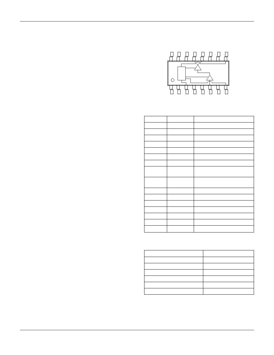
Pin Out Assignments
Pin 2: V
G2
Second stage gate voltage tap. Should be RF bypassed.
Pin 3: V
REF
Sets quiescent current of amplifier. Nominal value of
~4.1 V can be set, by voltage dividing from V
DBC
(5.8 V)
using resistors R1 and R2 as shown in the schematic.
Pin 4: V
DD1
Drain of stage 1. Requires matching inductor, good
RF bypassing and the +5.8 V nominal supply voltage.
Pin 5: GND
DC and RF ground.
Pin 6: RF In
50
RF input. Series inductor on input line improves input
match.
Pin 7: V
G1
First stage gate voltage tap. Requires good RF bypassing.
Pin 8: V
DBC
Bias controller supply voltage. Connect to +5.8 V
nominal supply voltage.
Pin 9: V
SS
Negative voltage for bias controller circuit. Nominally -4 V.
Pin 10: V
G3
Third stage gate voltage tap.
Requires good
RF bypassing.
Pin 12, 13: RF Out/V
DD3
RF output and bias feed for third stage drain. Output
matching is required to transform the optimum load
impedance to 50
. The circuit must also provide a path
for the +5.8 V nominal DC bias and have good
RF bypassing.
Pin 16: V
DD2
Second stage drain voltage. Requires matching inductor,
good RF bypassing and connection to the +5.8 V nominal
supply voltage.
1
2
3
4
5
6
7
8
16
15
14
13
12
11
10
9
Bias
Control
V
DD2
N/C N/C
RF
Out
N/C V
G3
V
SS
RF
Out
N/C V
G2
V
REF
V
DD1
RF In V
G1
V
DBC
GND
Pin Out
Pin Configuration
Terminal
Symbol
Function
1
N/C
Not Connected
2
V
G2
Gate Voltage 2
3
V
REF
Reference Voltage
4
V
DD1
Drain Voltage 1
5
GND
Ground
6
RF In
RF Input
7
V
G1
Gate Voltage 1
8
V
DBC
Positive Bias
Controller Supply Voltage
9
V
SS
Negative Bias
Controller Supply Voltage
10
V
G3
Gate Voltage 3
11
N/C
Not Connected
12
RF Out/V
DD3
RF Output/Drain Voltage 3
13
RF Out/V
DD3
RF Output/Drain Voltage 3
14
N/C
Not Connected
15
N/C
Not Connected
16
V
DD2
Drain Voltage 2
Characteristic
Value
Drain Voltage (V
DD
)
10 V
Bias Voltage (V
SS
)
-6 V
Reference Voltage (V
REF
)
6 V
Power Input (P
IN
)
12 dBm
Operating Temperature (T
OPT
)
-30 to +100∞C
Storage Temperature (T
STG
)
-35 to +120∞C
Absolute Maximum Ratings