 | –≠–ª–µ–∫—Ç—Ä–æ–Ω–Ω—ã–π –∫–æ–º–ø–æ–Ω–µ–Ω—Ç: CX65002 | –°–∫–∞—á–∞—Ç—å:  PDF PDF  ZIP ZIP |

Skyworks Solutions, Inc. ∑ Phone [781] 376-3000 ∑ Fax [781] 376-3100 ∑ sales@skyworksinc.com ∑ www.skyworksinc.com
101467E ∑ Skyworks Proprietary and Confidential information ∑ Products and Product Information are Subject to Change Without Notice ∑ October 11, 2004
1
DATA SHEET
CX65002: 700 ≠ 1400 MHz Linear Power Amplifier Driver
Applications
∑ AMPS/CDMA/TDMA/GSM handsets
∑ Wireless Local Loop (WLL) and Industrial, Scientific, Medical
(ISM) bands
∑ Repeaters
∑ Paging
∑ Mobile radios
∑ Telematics
∑ UHF TV broadcasts
Features
∑ 5 V single supply operation
∑ Linear P
OUT
of 24 dBm
∑ OIP3 of 46 dBm
∑ Excellent CDMA performance
∑ Internal bias circuits
∑ 8-pin SOIC 5.994 x 4.928 mm package with downset paddle
1
2
3
4
8
7
6
5
C1215
NC
VB
RFIN
Y
VCC1
RFOUT
RFOUT
VCC2
Figure 1. CX65002 Pinout ≠ 8-Pin SOIC Package
(Top View)
Description
Skyworks CX65002 power amplifier driver offers a desirable
combination of features that provide superb performance and
ease of use in a low-cost Surface-Mounted Technology (SMT)
package. The Gallium Arsenide (GaAs) Heterojunction Bipolar
Transistor (HBT) power amplifier driver was developed and
optimized for extreme linear performance in a variety of
applications. It is ideal as a driver or output stage for transceivers
and repeaters in AMPS/CDMA/TDMA/GSM paging base stations,
mobile radios, telematics, and many other applications.
The 8-pin Small Outline Integrated Circuit (SOIC) device package
and pinout are shown in Figure 1. Figure 2 shows a functional
block diagram for the CX65002. Signal pin assignments and
functional pin descriptions are provided in Table 1.
Driver Bias
Input Bias
VCC1
8
5
2
3
6
7
4
Y
VCC2
VB
RFIN
RFOUT
PA
C1216
Figure 2. CX65002 Functional Block Diagram

DATA SHEET ∑ CX65002
Skyworks Solutions, Inc. ∑ Phone [781] 376-3000 ∑ Fax [781] 376-3100 ∑ sales@skyworksinc.com ∑ www.skyworksinc.com
2
October 11, 2004 ∑ Skyworks Proprietary and Confidential information ∑ Products and Product Information are Subject to Change Without Notice ∑ 101467E
Table 1. CX65002 Signal Descriptions
Pin #
Name
Description
Pin #
Name
Description
1 NC
No
connection
5 VCC2
Supply
voltage
2
VB
Input bias for amplifier driver
6
RFOUT
RF output
3 RFIN
RF
input
7 RFOUT
RF
output
4
Y
Output of internal bias circuit
8
VCC1
Supply voltage
Table 2. CX65002 Absolute Maximum Ratings
Parameter Symbol
Min
Typical
Max
Units
RF input power
P
IN
10
dBm
Supply voltage (VCC1 and VCC2 pins)
VCC
5.5
V
Supply current (I
D
+ I
BIAS
) I
CC
240
mA
Power dissipation
1.3
W
Case operating temperature
T
C
≠40
+85
∞C
Storage temperature
T
ST
≠55
+125
∞C
Junction temperature
T
J
+150
∞C
Note: Exposure to maximum rating conditions for extended periods may reduce device reliability. There is no damage to device with only one parameter set at the limit and all other
parameters set at or below their nominal value.
Technical Description
The CX65002 is a single stage linear amplifier. The device can be
externally matched for optimum gain and linearity using two to
three passive components. These external components allow the
amplifier to be set to a desired operating frequency.
The CX65002 contains a bias circuit for optimum temperature
tracking performance. An external resistor is used to set the bias
current level. The value of this resistor can be selected to set the
amplifier operational mode to Class A, B, or AB.
Package and Handling Information
Since the device package is sensitive to moisture absorption, it is
baked and vacuum packed before shipping. Instructions on the
shipping container label regarding exposure to moisture after the
container seal is broken must be followed. Otherwise, problems
related to moisture absorption may occur when the part is
subjected to high temperature during solder assembly.
If the part is attached in a reflow oven, the temperature ramp rate
should not exceed 5
∞C per second. Maximum temperature
should not exceed 225
∞C and the time spent at a temperature
that exceeds 210
∞C should be limited to less than 10 seconds. If
the part is manually attached, precaution should be taken to
ensure that the part is not subjected to a temperature that
exceeds 300
∞C for more than 10 seconds.
Care must be taken when attaching this product, whether it is
done manually or in a production solder reflow environment.
Production quantities of this product are shipped in a standard
tape and reel format. For packaging details, refer to the Skyworks
Application Note, Tape and Reel, document number 101568.
Electrical and Mechanical Specifications
The absolute maximum ratings of the CX65002 are provided in
Table 2. The recommended operating conditions are specified in
Table 3 and electrical specifications are provided in Table 4.
Typical performance characteristics of the CX65002 are shown in
Figures 3 through 12. Figure 19 shows the package dimensions
for the 8-pin SOIC and Figure 20 provides the tape and reel
dimensions.
Electrostatic Discharge (ESD) Sensitivity
The CX65002 is a static-sensitive electronic device. Do not
operate or store near strong electrostatic fields. Take proper ESD
precautions.

DATA SHEET ∑ CX65002
Skyworks Solutions, Inc. ∑ Phone [781] 376-3000 ∑ Fax [781] 376-3100 ∑ sales@skyworksinc.com ∑ www.skyworksinc.com
101467E ∑ Skyworks Proprietary and Confidential information ∑ Products and Product Information are Subject to Change Without Notice ∑ October 11, 2004
3
Table 3. CX65002 Recommended Operating Conditions
Parameter Symbol
Min
Typical
Max
Units
Supply voltage (VCC1 and VCC2 pins)
VCC
5
V
Operating frequency
F
O
700
1400
MHz
Junction temperature
T
J
140
∞C
Maximum bias condition
(VCC
◊ I
D
) < (T
J
_
RECOMMENDED
≠ T
C
)/R
TH
,
J
-
C
Table 4. CX65002 Electrical Characteristics
(VCC = 5 V, T
C
= 25 ∞C)
Parameter Symbol
Test
Conditions Min
Typical
Max Units
OIP3 Match, Frequency = 900 MHz (Note 1)
Quiescent current (l
D
+ l
BIAS
) Iq
R
BIAS
= 270
120
130
mA
Small signal gain
G
P
IN
= ≠15 dBm
16.5
18
dB
Linear output power (Note 2)
P
OUT
P
IN
= +7 dBm
22.5
24
dBm
Power Added Efficiency
PAE
P
IN
= +7 dBm
34
38
%
Noise Figure (NF)
NF
5
6
dB
Output IP3
OIP3
Two CW tones with 1 MHz
spacing, P
IN
= ≠12 dBm
per tone
40 44 dBm
Thermal resistance (junction ≠ case)
R
TH
,
J
-
C
65
∞C/W
ACPR Match, Frequency = 881.5 MHz (Note 3)
Quiescent current (l
D
+ l
BIAS
) Iq
R
BIAS
= 270
115
135
mA
Small signal gain
G
P
IN
= ≠15 dBm
15.5
17
dB
Peak envelope power (Note 2)
P
PEP
IS95 downlink CDMA
signal, 9 ch Fwd,
P
IN
= 3 dBm
29 dBm
Average output power
@ ACPR = ≠45 dBc, 885 kHz offset
P
OUT
ACPR
IS95 downlink CDMA
signal, 9 ch Fwd,
P
IN
= 4.5 dBm
19.5 21.5 dBm
Note 1: Device matched for optimum OIP3 according to circuit shown in Figure 15.
Note 2: For reliable operation, do not violate the maximum input drive level specified in Table 2.
Note 3: Device matched for optimum ACPR according to circuit shown in Figure 16.
10
13
16
19
22
25
-6
-4
-2
0
2
4
6
8
Pin (dBm)
P
out (dB
m
)
-40C
25C
85C
Figure 3. Typical P
OUT
vs P
IN
@ 900 MHz Over Temperature (Circuit
Match for Optimum OIP3)
0
10
20
30
40
50
-6
-4
-2
0
2
4
6
8
Pin (dBm)
PAE (
%
)
-40C
25C
85C
Figure 4. Typical PAE vs P
IN
@ 900 MHz Over Temperature
(Circuit Match for Optimum OIP3)
DATA SHEET ∑ CX65002
Skyworks Solutions, Inc. ∑ Phone [781] 376-3000 ∑ Fax [781] 376-3100 ∑ sales@skyworksinc.com ∑ www.skyworksinc.com
4
October 11, 2004 ∑ Skyworks Proprietary and Confidential information ∑ Products and Product Information are Subject to Change Without Notice ∑ 101467E
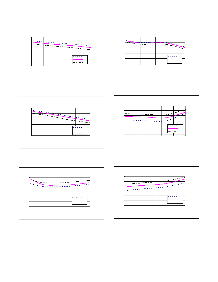
17
18
19
20
21
700
730
760
790
820
850
Freq (MHz)
Small Signal Gain (dB)
-40C
25C
85C
Figure 5. Typical Small Signal Gain From 700 to 850 MHz Over
Temperature (Circuit Match for Optimum Gain)
13
14
15
16
17
18
1100
1175
1250
1325
1400
Freq (MHz)
Small Signal Gain (dB)
-40C
25C
85C
Figure 7. Typical Small Signal Gain From 1.1 to 1.4 GHz Over
Temperature (Circuit Match for Optimum Gain)
0
1
2
3
4
5
6
850
877.5
905
932.5
960
Freq (MHz)
NF
(d
B)
-40C
25C
85C
Figure 9. Typical NF From 850 to 960 MHz Over Temperature
(Circuit Match for Optimum OIP3)
14
15
16
17
18
19
850
877.5
905
932.5
960
Freq (MHz)
Small Signal Gain (
d
B)
-40C
25C
85C
Figure 6. Typical Small Signal Gain From 850 to 960 MHz Over
Temperature (Circuit Match for Optimum OIP3)
0
1
2
3
4
5
6
700
730
760
790
820
850
Freq (MHz)
NF
(d
B)
-40C
25C
85C
Figure 8. Typical NF From 700 to 850 MHz Over Temperature
(Circuit Match for Optimum Gain)
0
1
2
3
4
5
6
1100
1175
1250
1325
1400
Freq (MHz)
NF
(d
B)
-40C
25C
85C
Figure 10. Typical NF From 1.1 to 1.4 GHz Over Temperature
(Circuit Match for Optimum Gain)

DATA SHEET ∑ CX65002
Skyworks Solutions, Inc. ∑ Phone [781] 376-3000 ∑ Fax [781] 376-3100 ∑ sales@skyworksinc.com ∑ www.skyworksinc.com
101467E ∑ Skyworks Proprietary and Confidential information ∑ Products and Product Information are Subject to Change Without Notice ∑ October 11, 2004
5
30
35
40
45
50
55
850
877.5
905
932.5
960
Freq (MHz)
OIP3 (dBm)
-40C
25C
85C
Figure 11. Typical OIP3 vs Frequency Over Temperature
(Circuit Match for Optimum OIP3)
-65
-60
-55
-50
-45
-40
10
12
14
16
18
20
22
24
Pout (dBm)
ACP
R (dBc
)
Figure 12. Typical ACPR vs P
OUT
@ 881.5 MHz, 750 kHz Offset,
25
∞C (Circuit Match for Optimum ACPR)
Evaluation Board Description
Skyworks CX65002 Evaluation Board is used to test the
performance of the CX65002 power amplifier driver. An
Evaluation Board schematic diagram, optimized for the 3
rd
Order
Output Intercept Point (OIP3), is shown in Figure 13. A schematic
diagram optimized for Adjacent Channel Power Rejection (ACPR)
is provided in Figure 14. The Evaluation Board assembly diagram
is shown in Figure 15 and the Evaluation Board layer detail is
shown in Figure 16. The mounting footprint for the CX65002 is
shown in Figure 17.
Circuit Design Configurations
The following design considerations are general in nature and
must be followed regardless of final use or configuration.
1. Paths to ground should be made as short as possible.
2. The ground pad of the CX65002 power amplifier has special
electrical and thermal grounding requirements. This pad is the
main thermal conduit for heat dissipation. Since the circuit
board acts as the heat sink, it must shunt as much heat as
possible from the amplifier. As such, design the connection to
the ground pad to dissipate the maximum wattage produced
to the circuit board. Multiple vias to the grounding layer are
required.
NOTE: Junction temperature (T
J
) of the device increases with a
poor connection to the slug and ground. This reduces the
lifetime of the device.
3. External bypass capacitors are required on the VCC line and
on pins 4, 5, and 8.
4. Bias resistor R1 is used to control the reference voltage of the
bias circuit (VCC1) at pin 8.
5. Inductor L2 is placed between the bias circuit output (pin 4)
and the base of the RF transistor (pin 2) for bias circuit and RF
transistor connection.
Suggested matching circuits are shown in Figures 13 and 14.
Testing Procedure
Use the following procedure to set up the CX65002 Evaluation
Board for testing. Refer to Figure 18 for guidance:
1. Connect a 5.0 V supply to VCC. If available, enable the current
limiting function of the power supply to 240 mA.
2. Connect a signal generator to the RF signal input port. Set it to
the desired RF frequency at a power level of ≠15 dBm or less
to the Evaluation Board but do NOT enable the RF signal.
3. Connect a spectrum analyzer to the RF signal output port.
4. Enable the power supply.
5. Enable the RF signal.
6. Take measurements.
CAUTION: If any of the input signals exceed the rated maximum
values, the CX65002 Evaluation Board can be
permanently damaged.