
Data Sheet
Skyworks
Doc. No. 101472D
Proprietary Information and Specifications Are Subject to Change
March 12, 2002
CX65101
1700 - 2200 MHz Linear Power Amplifier
Skyworks' CX65101 power amplifier is a fully matched 8-pin Leadless Chip Carrier
(LCC) surface mount module, developed for Personal Communications System
(PCS) and Wireless Local Loop (WLL) applications. This small, power-efficient
amplifier has a full 1700 to 2200 MHz bandwidth coverage packed into a single
compact package. All active circuitry in the module is contained in a single Gallium
Arsenide (GaAs) Microwave Monolithic Integrated Circuit (MMIC). This device is
manufactured with Skyworks' Aluminum (Al)GaAs Heterojunction Bipolar Transistor
(HBT) process, which allows for single supply operation while maintaining high
efficiency and good linearity.
Figure 1 shows a functional block diagram for the CX65101. The device package
and pinout are shown in Figure 2.
OUTPUT
MATCH
DA
DA
RFOUT
RFIN
GND
5, 7
6
2
V
CC1
V
CC2
4
3
INPUT MATCH
DRIVER STAGE
BIAS
INTERSTAGE
MATCH
POWER STAGE
BIAS
1
GND
VR
E
F
MMIC
MODULE
8
Figure 1. CX65101 Functional Block Diagram
Distinguishing Features
∑
Typical P
OUT
of 28.5 dBm
∑
High linearity
∑
Low power consumption
∑
8-pin LCC package
∑
Single +3.4 V supply
Applications
∑
PCS/DCS/UMTS
∑
Repeaters
∑
WLL, and Industrial, Scientific, Medical (ISM)
bands
∑
Mobile radio
∑
Telematics
GND
VREF
GND
GND
RFIN
V
CC2
V
CC1
RFOUT
1
2
3
4
5
6
7
8
Figure 2. CX65101 Pinout≠ 8-Pin LCC Package
Top View
CX65101
Power Amplifier
2
Skyworks
101472D
Proprietary Information and Specifications Are Subject to Change
March 12, 2002
Electrical and Mechanical Specifications
The signal pin assignments and functions are described in
Table 1. The absolute maximum ratings of the CX65101 are
provided in Table 2. The recommended operating conditions are
specified in Table 3 and electrical specifications are provided in
Table 4.
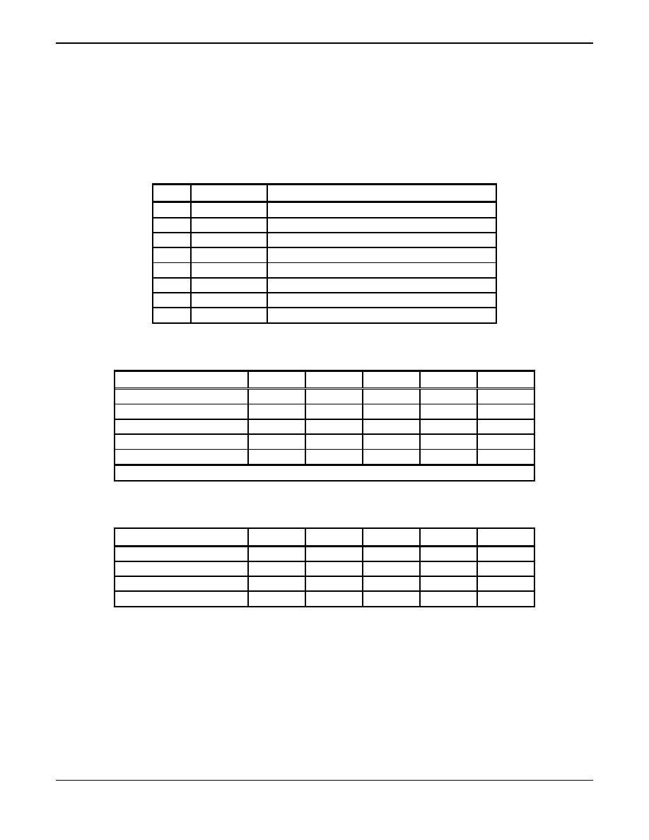
Typical performance characteristics over temperature of the
CX65101 are illustrated in Figures 3, 4, 5, 6, 7 and 8.
Table 1. CX65101 Signal Descriptions
Pin #
Name
Description
1 GND
Ground
2 RFIN
RF
input
3 VREF
Reference
voltage
4 VCC2
Supply
voltage
5 GND
Ground
6 RFOUT
RF
output
7 GND
Ground
8 VCC1
Supply
voltage
Table 2. CX65101 Absolute Maximum Ratings
Parameter Symbol
Min
Typical
Max
Units
RF input power
P
IN
10
dBm
Supply voltage
VCC
5
V
Reference voltage
V
REF
3.6 V
Case operating temperature
T
C
≠30 100 ∞C
Storage temperature
T
ST
≠55 125 ∞C
Note: No damage to device if only one parameter is applied at a time with other parameters at nominal conditions.
Table 3. CX65101 Recommended Operating Conditions
Parameter Symbol
Min
Typical
Max
Units
Supply voltage
VCC
3.4
V
Reference voltage
V
REF
3.3 V
Operating frequency
F
O
1700 1900 2200 MHz
Case operating temperature
T
C
≠30 25 85 ∞C
Power Amplifier
CX65101
101472D
Skyworks
3
March 12, 2002
Proprietary Information and Specifications Are Subject to Change
Table 4. CX65101 Electrical Characteristics
(VCC = 3.4 V, V
REF
= 3.3 V, Frequency = 1900 MHz, T
C
= 25 ∞C)
Parameter Symbol
Test
Conditions
Min Typical Max Units
Analog Inputs
Frequency
range
1700 1900 2200 MHz
Quiescent current
Iq
130
170
mA
Small signal gain
G
P
IN
= ≠15 dBm
20.0
21.5
dB
Output power
P
OUT
P
IN
= 7 dBm
27.5
28.5
dBm
Efficiency PAE
P
IN
= 7 dBm
27.5
30.0
%
Noise Figure (NF)
NF
5
6
dB
Output IP3
OIP3
Two tones with
100 kHz
spacing
P
IN
= 0 dBm
per tone
37 40 dBm
Note: The above specifications apply only to the 1900 MHz operating frequency.
24
25
26
27
28
29
30
3
4
5
6
7
8
Pin (dBm)
Pout
(
d
B
m
)
-30C
25C
85C
Figure 3. Typical P
OUT
vs P
IN
Over Temperature

CX65101
Power Amplifier
4
Skyworks
101472D
Proprietary Information and Specifications Are Subject to Change
March 12, 2002
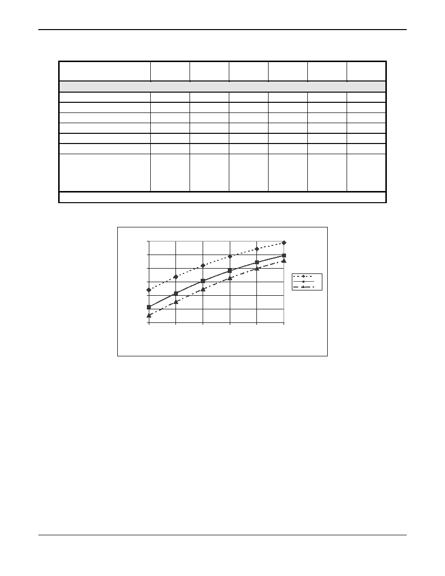
18
20
22
24
26
28
30
32
34
3
4
5
6
7
8
Pin (dBm)
PA
E (
%
)
-30C
25C
85C
Figure 4. Typical PAE vs P
IN
Over Temperature
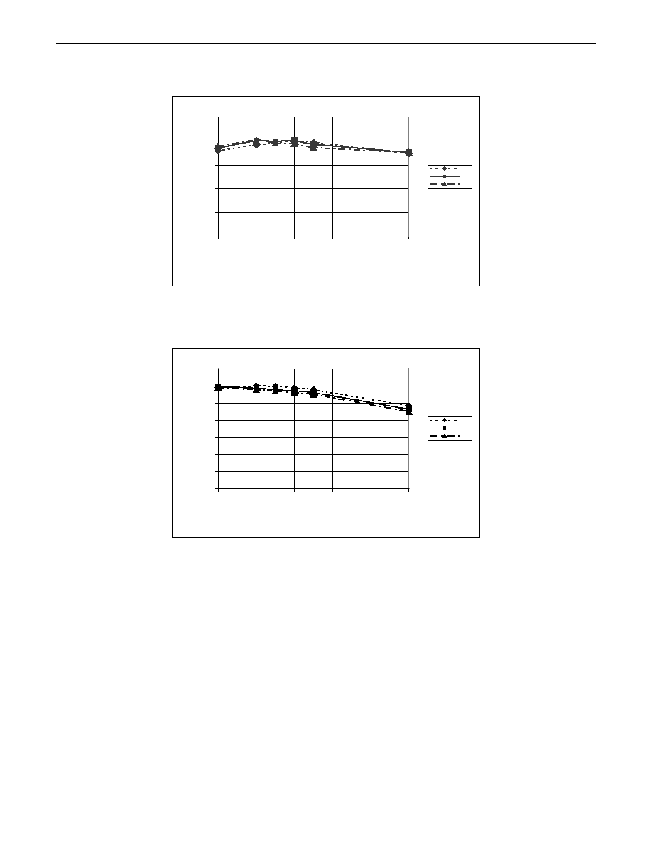
0
5
10
15
20
25
30
1700
1800
1900
2000
2100
2200
Freq (MHz)
Sma
ll Signa
l G
a
in (
d
B
)
-30C
25C
85C
Figure 5. Typical Small Signal Gain vs Frequency Over Temperature
0
1
2
3
4
5
6
7
8
1700
1800
1900
2000
2100
2200
Freq (MHz)
NF
(d
B)
-30C
25C
85C
Figure 6. Typical Noise Figure vs Frequency Over Temperature
Power Amplifier
CX65101
101472D
Skyworks
5
March 12, 2002
Proprietary Information and Specifications Are Subject to Change
0
10
20
30
40
50
1700
1800
1900
2000
2100
2200
Freq (MHz)
OI
P
3
(dBm
)
-30C
25C
85C
Figure 7. Typical OIP3 vs Frequency Over Temperature
0
5
10
15
20
25
30
35
1700
1800
1900
2000
2100
2200
Freq (MHz)
Pout
(
d
B
m
)
-30C
25C
85C
Figure 8. Typical P
OUT
vs Frequency Over Temperature
Evaluation Board Description
Skyworks' CX65101 Evaluation Board is used to test the
CX65101 power amplifier's performance. The CX65101
Evaluation Board schematic diagram is shown in Figure 9. The
schematic shows the basic design of the board for the 1700 to
2200 MHz range. Figure 10 provides the Evaluation Board
assembly diagram. Figure 11 provides the Evaluation Board
layer detail.
Circuit Design Considerations ________________________
The following design considerations are general in nature and
must be followed regardless of final use or configuration:
1. Paths to ground should be made as short as possible.
2. The ground pad of the CX65101 power amplifier has
special electrical and thermal grounding requirements. This
pad is the main thermal conduit for heat dissipation. Since
the circuit board acts as the heat sink, it must shunt as
much heat as possible from the amplifier. As such, design
the connection to the ground pad to dissipate the maximum
wattage produced to the circuit board. Multiple vias to the
grounding layer are required.
3. Two external output bypass capacitors, 0.01
µ
F and
4.7
µ
F, are required on the VCC1 (pin 8) supply input. The
same two capacitors are also required on the VCC2 (pin 4)
supply input. Both capacitors should be placed in parallel