Skyworks Solutions, Inc. ∑ Phone [781] 376-3000 ∑ Fax [781] 376-3100 ∑ sales@skyworksinc.com ∑ www.skyworksinc.com
200137 Rev. A ∑ Skyworks Proprietary Information ∑ Products and Product Information are Subject to Change Without Notice. ∑ February 7, 2005
1
Characteristic
Value
Operating temperature
-65 ∞C to +150 ∞C
Storage temperature
-65 ∞C to +200 ∞C
Power dissipation (derate
250 mW
linearly to zero @ 175 ∞C)
Typical lead strength
8 grams pull
Absolute Maximum Ratings
Features
Low capacitance
Low resistance
Fast switching
Oxide-nitride passivated
Durable construction
High voltage
Description
The DSG9500-000 is designed for low resistance, low capaci-
tance and fast switching time. The oxide-nitride passivation
layers provide reliable operation and stable junction parameters
that provide complete sealing of the junction permitting use in
assemblies with some degree of moisture sealing.
The DSG9500-000 is ideal for microstrip or stripline circuits and
for circuits requiring high isolation from a series mounted diode
such as broad band multi-throw switches, phase shifters, lim-
iters, attenuators and modulators.
DSG9500-000: Planar Beam Lead PIN Diode
DATA SHEET
Applications
Designed for switching applications
Performance is guaranteed only under the conditions listed in the specifications table and is
not guaranteed under the full range(s) described by the Absolute Maximum specifications.
Exceeding any of the absolute maximum/minimum specifications may result in permanent
damage to the device and will void the warranty.
CAUTION: Although this device is designed to be as robust as
possible, Electrostatic Discharge (ESD) can damage
this device. This device must be protected at all times
from ESD. Static charges may easily produce poten-
tials of several kilovolts on the human body or
equipment, which can discharge without detection.
Industry-standard ESD precautions must be employed
at all times.
Breakdown
Capacitance
Series Resistance
Minority Carrier
Voltage
Total @ 50 V,
(From Ins. Loss
Lifetime
RF Switching
Outline
Part
@ 10
µ
µA
1 MHz
@ 3 GHz, 50 mA)
(1)
I
F
= 10 mA,
Time
Drawing
Number
(V)
(pF)
(
)
I
R
= 6 mA (ns)
T
S
(ns)
(2)
Number
Min.
Max.
Max.
Typ.
DSG9500≠000
200
0.02
4.0
250
25
169-001
Low Capacitance Planar Beam Lead Diode
1. Total capacitance calculated from isolation at 9 GHz zero bias. Series resistance and capacitance are measured at microwave frequencies on a sample basis from each lot.
All diodes are characterized for capacitance at ≠50 V, 1 MHz, and series resistance at 1 KHz, 50 mA, measurements which correlate well with microwave measurements.
2. T
S
measured from RF transition, 90% to 10%, in series configuration.
DATA SHEET ∑ DSG9500-000
Skyworks Solutions, Inc. ∑ Phone [781] 376-3000 ∑ Fax [781] 376-3100 ∑ sales@skyworksinc.com ∑ www.skyworksinc.com
February 7, 2005 ∑ Skyworks Proprietary Information ∑ Products and Product Information are Subject to Change Without Notice. ∑ 200137 Rev. A
2
Duroid
Metal Conductor
Preferred Beam
Lead Orientation
Beam Lead Pin
0.005"
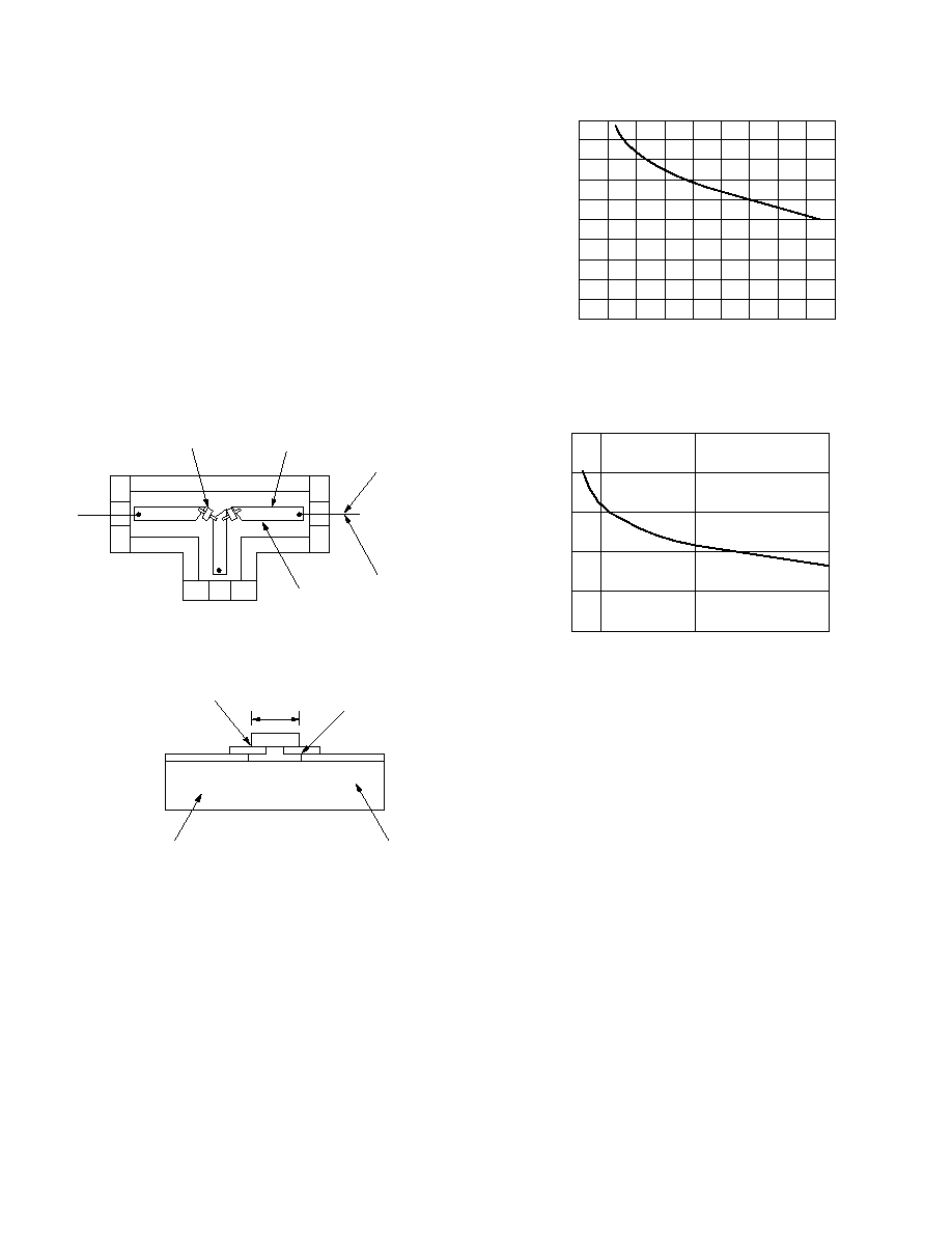
Figure 1. Typical SPDT Circuit Arrangement
Figure 2. Typical Beam Lead Mounting
Beam Lead Pin
Duroid Substrate
50
Glass Bead
Connecting
Lead
50
Transmission LIne
Isolation Loss (dB)
Frequency (GHz)
Figure 3. Isolation vs. Frequency, SPDT
0
2
4
6
8
10
12
14
16
18
0
8
4
12
16
20
24
28
32
36
38
Insertion Loss (dB)
Bias Current (mA)
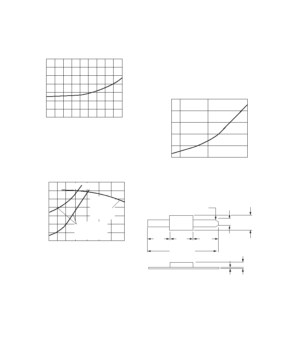
Figure 4. Diode Insertion Loss vs. Bias,
SPST 18 GHz
0
10
50
100
0.5
1.0
1.5
2.0
2.5
0
Performance Data for DSG9500≠000
Figures 1 and 2 show a single pole double-throw 1≠18 GHz
switch these diodes are mounted an Alumina, Duroid, or Teflon
fiberglass 50
microstrip circuits. Typical bonding methods
include thermal compression bonding, parallel gap welding, and
soldering.
SPDT isolation curves are shown in Figure 3 and insertion loss in
Figures 4 and 5. With proper transitions and bias circuits, VSWR
is better than 2.0 to 1 through 18 GHz.
Switching Considerations
The typical minority carrier lifetime of the DSG9500 diodes is
100 ns. With suitable drivers, the individual diodes can be
switched from high impedance (off) to low R
S
(on) in about 10 ns.
DATA SHEET ∑ DSG9500-000
Skyworks Solutions, Inc. ∑ Phone [781] 376-3000 ∑ Fax [781] 376-3100 ∑ sales@skyworksinc.com ∑ www.skyworksinc.com
200137 Rev. A ∑ Skyworks Proprietary Information ∑ Products and Product Information are Subject to Change Without Notice. ∑ February 7, 2005
3
Isolation Loss (dB)
Frequency (GHz)
Figure 5. Diode Insertion Loss vs. Frequency,
SPST 50 mA Bias00
0.2
0.4
0.6
0.8
1.0
0
1.2
0
2
4
6
8
10
12
14
16
18
1.4
CW Power (Milliwatts)
Frequency (GHz)
Figure 6. Typical Series Switch Behavior
at Room Temperature and Biased at
50 mA/1 V/4 V
50
100
200
500
1000
20
2000
0.1
0.2
0.5
1.0
2.0
5.0
10
20
5000
10% increase
in small signal
insertion loss
when biased at
50 mA
10% decrease in
small signal insertion
loss when biased at
≠1 V/≠4 V
0.4 V
0.1 V
Peak Power (W)
Reverse Bias (V)
Figure 7. Peak Power Handling,
SPST 1 GHz
0
10
50
100
20
40
60
80
100
0
Power Handling for DSG9500≠000
Beam lead diodes are not suitable for high power operation
because of high internal thermal impedance of about 600 ∞C/W.
For pulsed operation, the total RF plus bias voltage must not
exceed the rated breakdown. Skyworks has made high power
tests at 1 GHz with 1
µs pulses, 0.001 duty, with 200 V diodes.
With 50 mA forward bias, there is no increase in insertion loss
over the 0 dBm level with a peak power input of 50 W. In the
open state, reverse bias voltage is required to keep the diode
from "rectifying," with resultant decrease in isolation and pos-
sible failure. Figure 7 shows allowed peak power versus reverse
bias at 1 GHz. At this frequency, the required reverse voltage is
almost equal to the peak RF voltage; at high frequency, the bias
can be reduced somewhat. Experimentation is necessary.
With maximum CW power dissipation of 250 mW, the
DSG9500≠000 diodes are normally rated at 2 W CW with linear
derating between 25 ∞C and 150 ∞C. Figure 6 presents data on
CW power handling as a function of bias and frequency.
0.004 (0.10 mm)
0.002 (0.05 mm)
0.004 (0.10 mm)
0.002 (0.05 mm)
0.035 (0.89 mm)
0.033 (0.84 mm)
0.007
(0.18 mm)
Max.
0.0005
(0.013 mm)
Max.
0.010
(0.25 mm)
Min.
0.010
(0.25 mm)
Min.
0.011
(0.28 mm)
Max.
Cathode End Has
Blunted Point
169-001

DATA SHEET ∑ DSG9500-000
Skyworks Solutions, Inc. ∑ Phone [781] 376-3000 ∑ Fax [781] 376-3100 ∑ sales@skyworksinc.com ∑ www.skyworksinc.com
February 7, 2005 ∑ Skyworks Proprietary Information ∑ Products and Product Information are Subject to Change Without Notice. ∑ 200137 Rev. A
4
Beam-Lead Diodes
Handling
Due to their small size, beam-lead devices are fragile and should
be handled with extreme care. The individual plastic packages
should be handled and opened carefully, so that no undue
mechanical strain is applied to the packaged device. It is recom-
mended that the beam-lead devices be handled through use of a
vacuum pencil using an appropriate size vacuum needle or a
pointed wooden stick such as a sharpened Q-tip or match stick.
The device will adhere to the point and can easily be removed
from the container and positioned accurately for bonding without
damage. Such handling should be done under a binocular micro-
scope with magnification in the range of 20X to 30X.
Special handling precautions are also required to avoid electrical
damage, such as static discharge.
Bonding
The DSG9500-000 can best be bonded to substrates by means of
thermocompression bonding. Essentially this type of bonding
involves pressing the gold beam of the device against the gold
plated metalized substrate under proper conditions of heat and
pressure so that a metallurgical bond joint between the two
occurs.
Procedure
The beam-lead devices to be bonded should be placed on a
clean, hard surface such as a microscope slide. It is recom-
mended that the beam side of the device be down so that this
side will be toward the substrate when bonded. The device can
be picked up by pressing lightly against one beam with the
heated tip. The substrate can then be appropriately positioned
under the tip and the device brought down against the substrate,
with proper pressure applied by means of the weld head.
A bonding tip temperature in the 350 ∞C to 450 ∞C range is rec-
ommended along with a bonding force of 50 to 70 grams. The
bonding time is in the range of 2 to 3 seconds. Optimum bonding
conditions should be determined by trial and error to compensate
for slight variations in the condition of the substrate, bonding tip,
and the type of device being bonded.
Equipment
The heat and pressure are obtained through use of a silicon car-
bide bonding tip with a radius of two to three mils. Such an item
is available from several commercial sources. In order to supply
the required tip-travel and apply proper pressure, a standard
miniature weld head can be used. Also available is a heated
wedge shank which is held by the weld head and in turn holds
the tip and supplies heat to it. The wedge shank is heated by
means of a simple AC power supply or a pulse type heated tool.
Substrate
For optimum bonding a gold plated surface at least 100
microinches thick is necessary. Although it is possible to bond to
relatively soft metalized substrate material such as epoxy-fiber-
glass, etc., optimum bonding occurs when a hard material such
as ceramic can be used.
Quality
If a good bond has been obtained, it is impossible to separate the
beam-lead device from the metalized substrate without damage.
If the device is destructively removed, the beam will tear away,
leaving the bonded portion attached to the substrate.
Beam≠Lead Packaging
The DSG-9500-000 is shipped in 2" x 2" black gel packs. The
beam-leads are mounted on the gel, the devices are covered
with a piece of lint-free release paper, on top of which is placed
a piece of conductive foam.

DATA SHEET ∑ DSG9500-000
Skyworks Solutions, Inc. ∑ Phone [781] 376-3000 ∑ Fax [781] 376-3100 ∑ sales@skyworksinc.com ∑ www.skyworksinc.com
200137 Rev. A ∑ Skyworks Proprietary Information ∑ Products and Product Information are Subject to Change Without Notice. ∑ February 7, 2005
5
Copyright © 2002, 2003, 2004, 2005, Skyworks Solutions, Inc. All Rights Reserved.
Information in this document is provided in connection with Skyworks Solutions, Inc. ("Skyworks") products. These materials are provided by Skyworks as a service to its customers and may be
used for informational purposes only by the customer. Skyworks assumes no responsibility for errors or omissions in these materials. Skyworks may make changes to its documentation, products,
specifications and product descriptions at any time, without notice. Skyworks makes no commitment to update the information and shall have no responsibility whatsoever for conflicts,
incompatibilities, or other difficulties arising from future changes to its documentation, products, specifications and product descriptions.
No license, express or implied, by estoppel or otherwise, to any intellectual property rights is granted by or under this document. Except as may be provided in Skyworks Terms and Conditions of
Sale for such products, Skyworks assumes no liability whatsoever in association with its documentation, products, specifications and product descriptions.
THESE MATERIALS ARE PROVIDED "AS IS" WITHOUT WARRANTY OF ANY KIND, EITHER EXPRESS OR IMPLIED OR OTHERWISE, RELATING TO SALE AND/OR USE OF SKYWORKS PRODUCTS INCLUDING
WARRANTIES RELATING TO FITNESS FOR A PARTICULAR PURPOSE, MERCHANTABILITY, PERFORMANCE, QUALITY OR NON-INFRINGEMENT OF ANY PATENT, COPYRIGHT OR OTHER INTELLECTUAL
PROPERTY RIGHT. SKYWORKS FURTHER DOES NOT WARRANT THE ACCURACY OR COMPLETENESS OF THE INFORMATION, TEXT, GRAPHICS OR OTHER ITEMS CONTAINED WITHIN THESE MATERIALS.
SKYWORKS SHALL NOT BE LIABLE FOR ANY DAMAGES, INCLUDING SPECIAL, INDIRECT, INCIDENTAL, OR CONSEQUENTIAL DAMAGES, INCLUDING WITHOUT LIMITATION, LOST REVENUES OR LOST
PROFITS THAT MAY RESULT FROM THE USE OF THESE MATERIALS WHETHER OR NOT THE RECIPIENT OF MATERIALS HAS BEEN ADVISED OF THE POSSIBILITY OF SUCH DAMAGE.
Skyworks products are not intended for use in medical, lifesaving or life-sustaining applications. Skyworks customers using or selling Skyworks products for use in such applications do so at their
own risk and agree to fully indemnify Skyworks for any damages resulting from such improper use or sale.
The following are trademarks of Skyworks Solutions, Inc.: Skyworks
Æ
, the Skyworks logo, and Breakthrough Simplicity
Æ
. Product names or services listed in this publication are for identification
purposes only, and may be trademarks of Skyworks or other third parties. Third-party brands and names are the property of their respective owners. Additional information, posted at
www.skyworksinc.com, is incorporated by reference.