 | ÐлекÑÑоннÑй компоненÑ: RM008 | СкаÑаÑÑ:  PDF PDF  ZIP ZIP |
100781d.book
Data Sheet
Skyworks Solutions, Inc. Proprietary
100781D
© 19992002 Skyworks Solutions, Inc., All Rights Reserved.
July 26, 2002
RM008
PA Module for Dual-band GSM900 and DCS1800 Applications
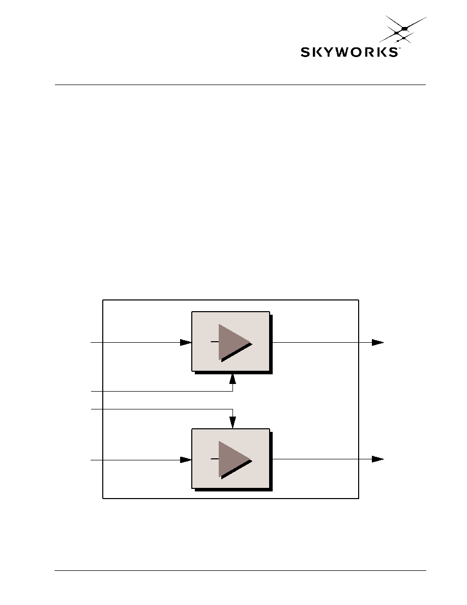
The RM008 is a dual-band Power Amplifier Module (PAM) designed in a compact
form factor for Class 4 GSM900 and Class 1 DCS1800 operation.
The PAM consists of two Gallium Arsenide (GaAs) Heterojunction Bipolar Transistor
(HBT) power amplifiers and internal components that match the RF input and output
ports to 50 ohms, which reduces the number of external components for a dual-band
design. Optimized for lithium-ion battery operation, both PAs share common power
supply pins to distribute current. The RM008 dual PAM has extremely low standby
current, which maximizes handset standby time.
A block diagram of the RM008 is shown below. The Analog Power Control (APC) pins
(GSM APC and DCS APC), control output power level. Table 4 of this data sheet
shows the complete signal pin assignments and descriptions of the RM008
dual-band Power Amplifier Module.
Functional Block Diagram
HBT
DCS IN
DCS OUT
GSM OUT
GSM IN
DCS APC
GSM APC
HBT
Distinguishing Features
·
High efficiency
GSM 50%
DCS 45%
·
Input and output matching
50 ohms internal
·
Small outline
9.1 mm x 11.61 mm
·
Low profile
1.64 mm
Applications
·
Class 4 GSM900 and Class 1
DCS1800 dual-band cellular
handsets
Electrical Characteristics
RM008
PA Module for Dual-band GSM900 and DCS1800 Applications
2
Skyworks Solutions, Inc. Proprietary
100781D
July 26, 2002
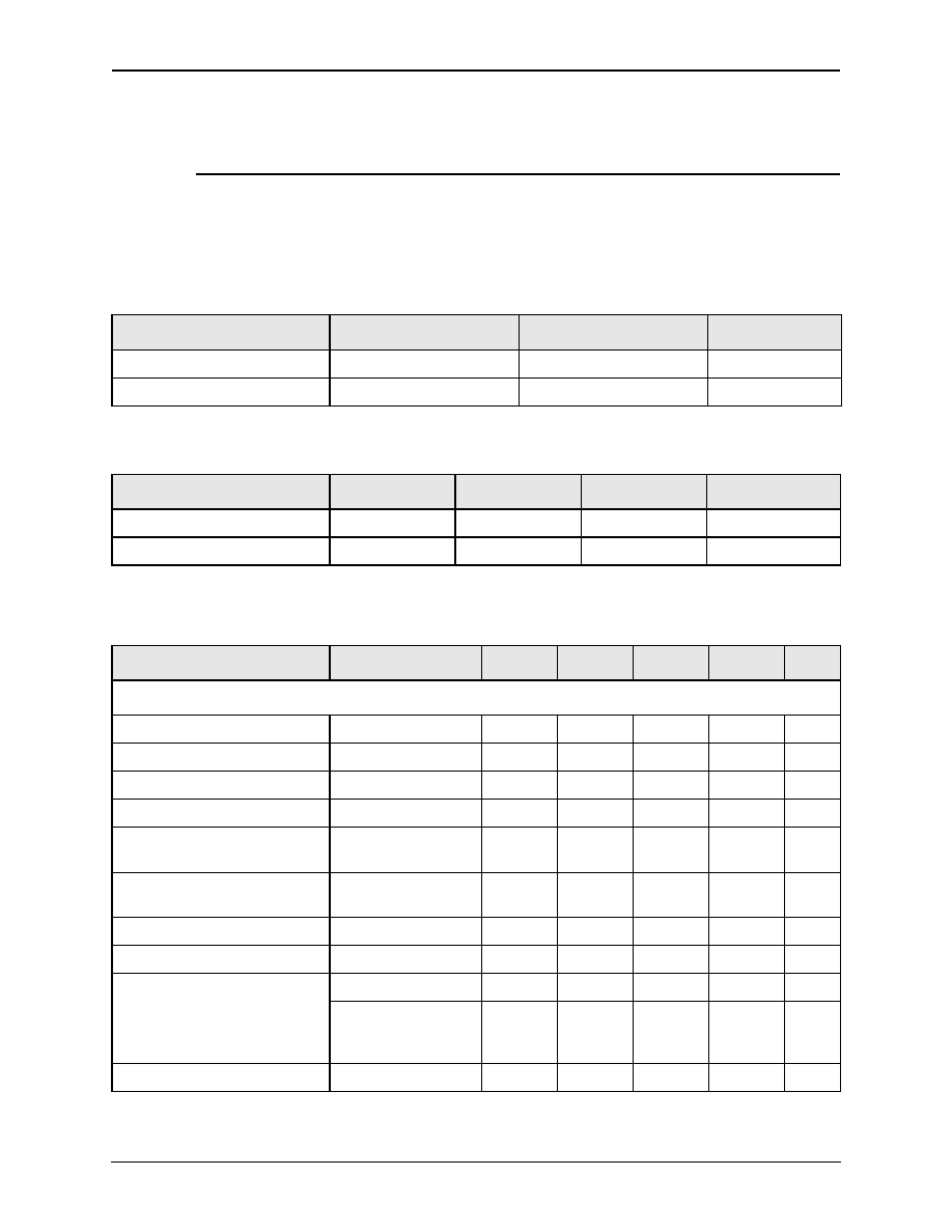
Electrical Characteristics
The following tables list the electrical characteristics of the RM008 Power Amplifier.
Table 1
depicts the absolute maximum ratings and
Table 2
specifies the recommended operating conditions
to achieve the performance specifications in
Table 3
.
Table 1. Absolute Maximum Ratings
Parameter
Minimum
Maximum
Units
Supply Voltage (V
CC
)
--
7
V
Storage Temperature
55
+125
°C
Table 2. Recommended Operating Conditions
Parameter
Minimum
Typical
Maximum
Units
Supply Voltage (V
CC
)
2.9
3.3
4.6
V
Temperature
30
--
+85
°C
Table 3. Electrical Specifications for Nominal Operating Conditions (1 of 2)
Parameter
Test Conditions
Symbol
Minimum
Typical
Maximum
Units
GSM Mode (f = 880915 MHz and P
IN
= 8 to 13 dBm)
Frequency Range
--
f1
880
--
915
MHz
Input Power
--
P
INGSM
8
10
13
dBm
Control Voltage Range
V
GSMAPC
V
APC
0.2
--
2.5
V
Control Current Into V
APC
--
l
GSMAPC
--
40
70
mA
Leakage Current
V
CC
= 4.6 V
V
APC
= 0 V
I
LEAKAGE
--
--
25
µA
Efficiency P
INGSM
= 10 dBm
P
OUTGSM
= 34 dBm
GSM
--
50
--
%
2nd Harmonic Distortion
P
OUTGSM
= 34.5 dBm
H
2GSM
--
--
5
dBm
3rd7th Harmonic Distortion
P
OUTGSM
= 34.5 dBm
H3H7
--
--
7
dBm
Output Power
P
INGSM
= 10 dBm
P
OUTGSM
34.0
34.5
--
dBm
P
INGSM
= 10 dBm
V
CC
= 2.9 V
T
CASE
= 30 °C to +85 °C
P
OUTDCS
32.5
33.0
--
dBm
Input VSWR
All
VSWR
(IN)
--
1.5:1
2:1
--
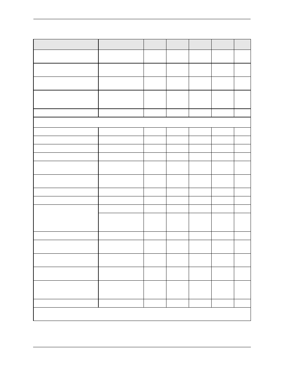
RM008
Electrical Characteristics
PA Module for Dual-band GSM900 and DCS1800 Applications
100781D
Skyworks Solutions, Inc. Proprietary
3
July 26, 2002
Isolation
P
INGSM
= 10 dBm
APC = 0.5 V
--
--
--
30
dBm
Stability Condition VSWR(load) (no
spurious oscillation > 35 dBm)
--
--
--
--
8:1
all angles
--
Load Mismatch VSWR(load) (no
damage/degradation)
--
--
--
--
10:1
all angles
--
Noise Floor
P
INGSM
= 10 dBm
BW = 100 kHz
f
O
±20 MHz offset
--
--
--
85
dBm
Full Power Control Voltage
P
OUTGSM
= 34.5 dBm
--
--
2.0
--
--
DCS Mode (f = 17101785 MHz and P
IN
= 6 to 11 dBm)
Frequency Range
--
f2
1710
--
1785
MHz
Input Power
--
P
INDCS
6
8.0
11
dBm
Control Voltage Range
V
DCSAPC
V
APC
0.2
--
2.5
V
Control Current Into V
APC
--
l
DCSAPC
--
30
70
mA
Leakage Current
V
CC
= 4.6 V
V
APC
= 0 V
I
LEAKAGE
--
--
25
µA
Efficiency
P
INDCS
= 8 dBm
P
OUTDCS
= 32 dBm
DCS
--
45
--
%
2nd Harmonic Distortion
P
OUTDCS
= 32.5 dBm
H
2DCS
--
--
7
dBm
3rd7th Harmonic Distortion
P
OUTDCS
= 32.5 dBm
H3H7
--
--
7
dBm
Output Power
P
INDCS
= 8 dBm
P
OUTDCS
32.0
32.5
--
dBm
P
INDCS
= 8 dBm
V
CC
= 2.9 V
T
CASE
= 30 °C to +85 °C
P
OUTDCS
30.5
31.0
--
dBm
Input VSWR
All
VSWR
(IN)
--
1.5:1
2:1
--
Isolation
P
INDCS
= 8 dBm
APC = 0.5 V
--
--
--
35
dBm
Stability Condition VSWR (load) no
spurious oscillation > 35 dBm)
--
--
--
--
8:1
all angles
--
Load Mismatch VSWR(load) (no
damage/degradation)
--
--
--
--
10:1
all angles
--
Noise Floor DCS1800
P
INDCS
= 8 dBm
BW = 100 kHz
f
O
±20 MHz offset
--
--
--
77
dBm
Full Power Control Voltage
P
OUTDCS
= 32.5 dBm
--
--
2.0
--
--
NOTE(S):
T
CASE
= 25 °C, RL = 50
, pulsed operation with pulse width = 577 µsec and duty cycle of 1:8, V
CC
= 3.3 V unless specified
otherwise
Table 3. Electrical Specifications for Nominal Operating Conditions (2 of 2)
Parameter
Test Conditions
Symbol
Minimum
Typical
Maximum
Units
Electrical Characteristics
RM008
PA Module for Dual-band GSM900 and DCS1800 Applications
4
Skyworks Solutions, Inc. Proprietary
100781D
July 26, 2002
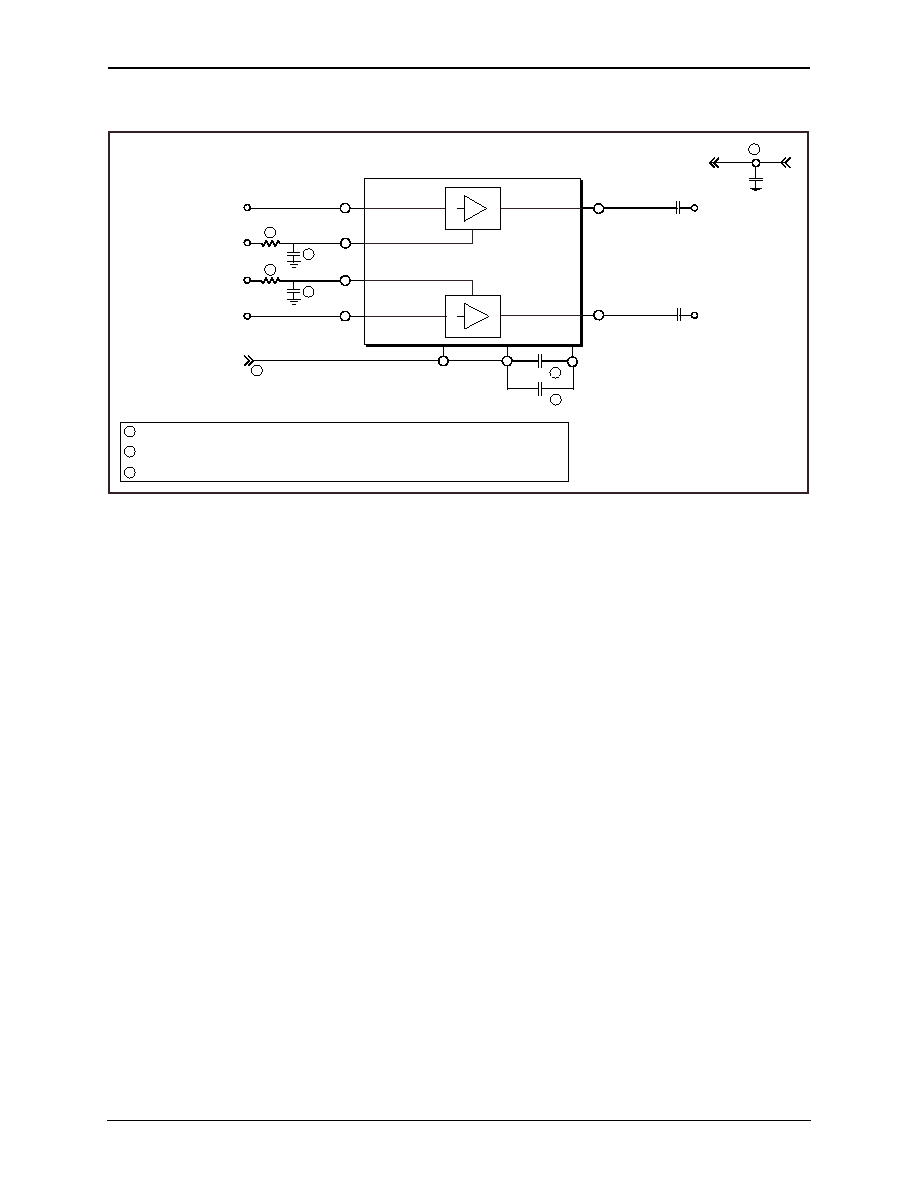
Figure 1. Typical RM008 PAM Application
DCS APC from PAC
G S M I N
DCS IN
G S M A P C f r o m P A C
10 pF
33 pF
DCS OUT
G S M O U T
2
4
1 0
1 2
1 6
1 4
VCC2
VCC1
8
6
101585_003
10 nF
100 pF
9
GND
10
µF
TANTALUM
Vbat
C
A
A
B
B
Vcc
Place caps at closest proximity to PA module with the capacitor ground directly connected to the PAM grounds.
Optional depending on PAC circuit.
Common connect Vbat to all Vcc pins.
A
B
C
C
HBT
HBT
B
B
G S M A P C
DCS APC
RM008
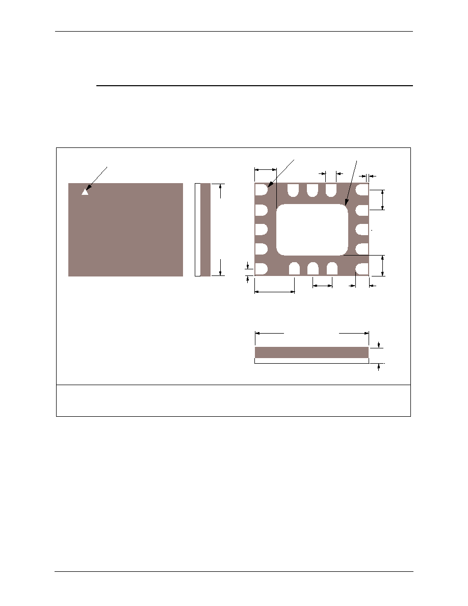
Package Dimensions and Pin Descriptions
PA Module for Dual-band GSM900 and DCS1800 Applications
100781D
Skyworks Solutions, Inc. Proprietary
5
July 26, 2002
Package Dimensions and Pin Descriptions
Figure 2
provides the package dimensions for the 16-pin RM008 leadless MCM.
Figure 3
shows
the device pin configuration and
Table 4
lists the pins and signal descriptions.
Figure 2. RM008 Package Dimensions--16-pin PAM (All Views)
SIDE VIEW
TOP VIEW
BOTTOM VIEW
FRONT VIEW
R0.381 Typ
0.762 Typ
1.02 Typ
2.286 ± 0.051
2.286 ± 0.051
PIN 1
0.127 Ref
1.905 ± 0.051
3.899 ± 0.051
1.64 max.
R0.860 Typ
NOTE(S):
1. All contact points are gold plated, lead free-surfaces.
2. All dimensions are in millimeters.
9.10 +0.20, -0.08
11.60 +0.20, -0.08
1.905 ± 0.051
0.737 ± 0.051
100781_004
Document Outline