
Data Sheet
Skyworks ≠ Preliminary
Doc. No. 101907A
Proprietary Information and Specifications Are Subject to Change
November 11, 2002
SKY73001
2-3500 MHz Direct Conversion Mixer
Skyworks' SKY73001 direct conversion mixer is an integrated, high-dynamic range,
zero Intermediate Frequency (IF) architecture down-converter for use in wireless
communication applications. High second and third order intercept points (IIP2 and
IIP3, respectively) allow seamless integration into high performance systems. The
SKY73001 has a wide RF and Local Oscillator (LO) frequency range of 2 to
3500 MHz.
Figure 1 shows a functional block diagram for the SKY73001. The device package
and pinout for the 32-pin Radio Frequency Land Grid Array (RFLGATM) are shown
in Figure 2.
C1267
LOI+
LOI≠
LOQ+
LOQ≠
RF+
RF≠
IFI+
IFI≠
IFQ+
IFQ≠
Figure 1. SKY73001 Functional Block Diagram
Distinguishing Features
∑
High second and third order Input Intercept Points
(IIP2 and IIP3)
∑
Wideband RF and LO input frequency range
(2 to 3500 MHz)
∑
Single +3.0 V supply
∑
≠40
∞
C to +85
∞
C operating temperature range
∑
Zero IF architecture eliminates need for image
rejection filter
∑
Differential IF output supports direct interface to
A/D circuitry
∑
AM demodulation immunity
∑
Low power consumption
∑
32-pin RFLGA package
Applications
∑
Personal Communications Systems (PCS)
∑
Digital Communications Systems (DCS)
∑
Global System for Mobile Communications (GSM)
∑
Third Generation (3G) wireless communications
∑
Mobile base stations
∑
Wireless Local Loops (WLLs)
∑
Wireless Local Area Networks (WLANs)
∑
Direct conversion receivers
C1266
GND
GND
GND
VCC
VCC
VCC
GND
GND
GND
25
24
23
22
21
20
19
18
17
LOIN
GND
LOIP
LOQN
GND
LOQP
GND
32
31
30
26
29
28
27
GND
GND
RFP
GND
GND
RFN
GND
10
11
12
16
13
14
15
GND
IFIP
GND
IFIN
GND
IFQP
GND
IFQN
GND
1
2
3
4
5
6
7
8
9
Figure 2. SKY73001 Pinout≠ 32-Pin RFLGA
Package (Top View)
SKY73001
Mixer
2
Skyworks ≠ Preliminary
101907A
Proprietary Information and Specifications Are Subject to Change
November 11, 2002
Electrical and Mechanical Specifications
The signal pin assignments and functions are described in
Table 1. The absolute maximum ratings of the SKY73001 are
provided in Table 2. The recommended operating conditions are
specified in Table 3 and electrical specifications are provided in
Table 4.
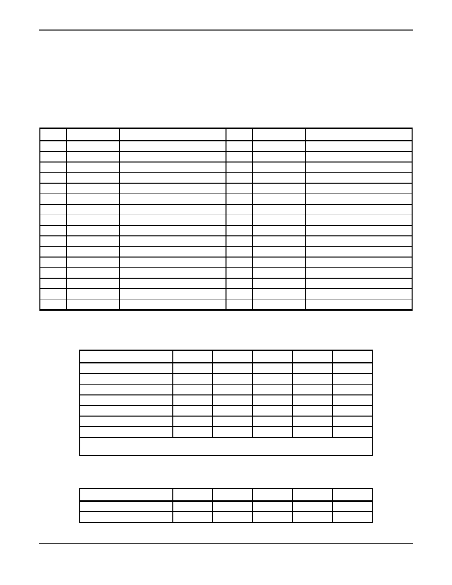
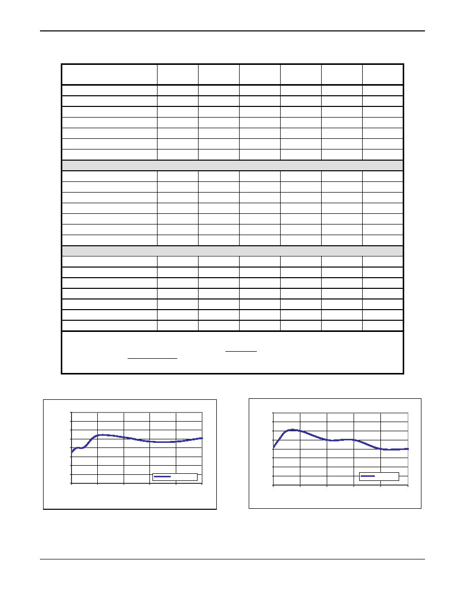
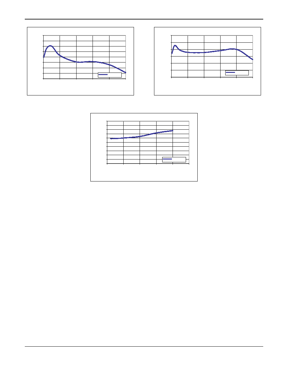
Typical performance characteristics of the SKY73001 with respect
to varying conditions are illustrated in Figures 3, 4, 5, 6, and 7.
Table 1. SKY73001 Signal Descriptions
Pin #
Name
Description
Pin #
Name
Description
1
GND Ground
17
GND Ground
2
GND
Ground
18
IFQN
Negative quadrature IF output
3
GND Ground
19
GND Ground
4
VCC
+3 VDC supply
20
IFQP
Positive quadrature IF output
5
VCC
+3 VDC supply
21
GND
Ground
6
VCC
+3 VDC supply
22
IFIN
Negative in-phase IF output
7
GND Ground
23
GND Ground
8
GND
Ground
24
IFIP
Positive in-phase IF output
9
GND Ground
25
GND Ground
10
LOIN
Negative LO input
26
GND
Ground
11 GND
Ground
27 GND
Ground
12
LOIP
Positive LO input
28
RFN
Negative RF input
13 GND
Ground
29 GND
Ground
14
LOQP
Positive quadrature LO input
30
RFP
Positive RF input
15 GND
Ground
31 GND
Ground
16
LOQN
Negative quadrature LO input
32
GND
Ground
Table 2. SKY73001 Absolute Maximum Ratings
(T
A
= +25
∞
∞
∞
∞
C, unless otherwise noted)
Parameter Symbol
Min
Typical
Max
Units
+3 V supply voltage
VCC
2.7
3.6
V
Power dissipation
140
230
mW
RF input power
+20
dBm
LO input power
+3
dBm
Thermal resistance
jc
36 ∞C/W
Operating case temperature
≠40
+85
∞C
Storage case temperature
≠40
0
+125
∞C
Note: Exposure to maximum rating conditions for extended periods may reduce device reliability. There is no damage to device
with only one parameter set at the limit and all other parameters set at or below their nominal values.
Table 3. SKY73001 Recommended Operating Conditions
Parameter Symbol
Min
Typical
Max
Units
+3 V supply voltage
VCC
2.7
3.0
3.3
V
Operating case temperature
≠40
+85
∞C
Mixer
SKY73001
101907A
Skyworks ≠ Preliminary
3
November 11, 2002
Proprietary Information and Specifications Are Subject to Change
Table 4. SKY73001 Electrical Characteristics
(IF = 10 MHz, LO input power = 0 dBm, T
C
= 25 ∞C unless otherwise noted)
Parameter Symbol
Test
Conditions
Min Typical Max Units
RF input frequency range
2
3500
MHz
LO input frequency range
2
3500
MHz
IF frequency range
DC
100
MHz
I/Q amplitude imbalance
≠0.3
+0.3
dB
I/Q phase error
1
deg
Image
rejection
(Note
1)
dB
IF output impedance
500
RF Input (900 MHz)
Voltage conversion gain
≠3
≠1
dBV
SSB Noise Figure
16
19
dB
IIP2
67
dBm
IIP3
23 26 dBm
≠1 dB compression point
13
15
dBm
RF input impedance
1.5:1
2.0:1
VSWR
LO input impedance
1.5:1
2.0:1
VSWR
RF Input (1900 MHz)
Voltage conversion gain
≠3.5
≠1.5
dBV
SSB Noise Figure
17.5
20.5
dB
IIP2
70
dBm
IIP3
22 25 dBm
≠1 dB compression point
12
14
dBm
RF input impedance
1.5:1
2.0:1
VSWR
LO input impedance
1.5:1
2.0:1
VSWR
Note 1: Image rejection is determined using the following equation:
[ ]
[ ]
˜
˜
¯
ˆ
Á
Á
Ë
Ê
-
+
+
+
=
cos
A
2
2
A
1
cos
A
2
2
A
1
log
10
IR
where
˜
˜
¯
ˆ
Á
Á
Ë
Ê
-
=
20
error
amplitude
10
A
in dB.
-6.0
-5.0
-4.0
-3.0
-2.0
-1.0
0.0
1.0
2.0
0
500
1000
1500
2000
2500
Frequency (MHz)
Conversion Gain (dBV)
IF = 10 MHz
Figure 3. Voltage Conversion Gain vs Frequency
10
11
12
13
14
15
16
17
18
0
500
1000
1500
2000
2500
Frequency (MHz)
Co
m
p
P
t
(
d
Bm
)
IF = 10 MHz
Figure 4. 1 dB Compression Point vs Frequency
SKY73001
Mixer
4
Skyworks ≠ Preliminary
101907A
Proprietary Information and Specifications Are Subject to Change
November 11, 2002
20.0
22.0
24.0
26.0
28.0
30.0
32.0
34.0
36.0
0
500
1000
1500
2000
2500
Frequency (MHz)
IIP3 (dBm
)
IF = 10 MHz
Figure 5. IIP3 vs Frequency (100 kHz Tone Spacing)
50.0
55.0
60.0
65.0
70.0
75.0
80.0
0
500
1000
1500
2000
2500
Frequency (MHz)
IIP2 (dBm
)
IF = 10 MHz
Figure 6. IIP2 vs Frequency
10.0
11.0
12.0
13.0
14.0
15.0
16.0
17.0
18.0
19.0
20.0
0
500
1000
1500
2000
2500
Frequency (MHz)
NF (
d
B)
IF = 10 MHz
Figure 7. Noise Figure vs Frequency (IF = 10 MHz)
Evaluation Board Description
Skyworks' SKY73001 Evaluation Board is used to test the
SKY73001 mixer's performance. The SKY73001 Evaluation
Board schematic diagram is shown in Figure 8. Figure 9
provides the Evaluation Board assembly diagram.
Circuit Design Considerations ________________________
The following design considerations are general in nature and
must be followed regardless of final use or configuration:
1. Paths to ground should be made as short as possible.
2. The ground pad of the SKY73001 direct conversion mixer
has special electrical and thermal grounding requirements.
This pad is the main thermal conduit for heat dissipation.
Since the circuit board acts as the heat sink, it must shunt
as much heat as possible from the mixer. As such, design
the connection to the ground pad to dissipate the maximum
wattage produced to the circuit board. Multiple vias to the
grounding layer are required.
3. Two external output bypass capacitors are required on the
VCC pin. The values of these capacitors will change with
respect to the desired RF frequency. One capacitor should
be used for low frequency bypassing and the other
capacitor for high frequency bypassing. Special attention
should be given so that the smaller value capacitor does
not go into self-resonance at the desired RF frequency.
See Figure 8 for a detailed diagram.
4. Wire wound balanced transformers (baluns) were used
during the test and characterization of the SKY73001.
Ceramic baluns can be used to create the differential input
signals (i.e., RF and LO). However, their performance will
limit the overall system performance of the SKY73001.
Testing Procedure ___________________________________
Use the following procedure to set up the SKY73001 Evaluation
Board for testing. Refer to Figure 10 for guidance:
1. Connect the SKY73001 Evaluation Board to a +3.0 VDC
power supply using an insulated supply cable. If available,
enable the current limiting function of the power supply to
100 mA for the +3 VDC supply current.
2. Connect a signal generator to the RF signal input port. Set
it to the desired RF frequency at a power level of 0 dBm but
do NOT enable.

Mixer
SKY73001
101907A
Skyworks ≠ Preliminary
5
November 11, 2002
Proprietary Information and Specifications Are Subject to Change
C1318
2-Pin Header
SKY73001
TCM-4-25
TCM-9-16
TCM-9-16
TCM-4-25
TCM-4-25
RF
SMA
IFIP
I_IF
Q_IF
Q_LO
I_LO
LOIN
LOIP
LOQP
LOQN
IFIN
IFQP
IFQN
C1
33 pF
C2
1000 pF
GND
GND
GND
RFP
RFN
GND
VCC
1
2
3
2
1
6
1
SMA
1
SMA
SMA
SMA
1
1
1
1
4
4
2
3
25
24
23
22
21
20
19
18
17
1
2
3
4
5
6
7
32
31
30
29
28
27
26
10
33
Pin 33
11
12
13
14
15
16
8
9
1
6
6
4
4
1
2
3
1
2
3
2
3
4
GND
Figure 8. SKY73001 Evaluation Board Schematic
3. Connect a signal generator to the LOQ signal input port.
Set to the desired LO frequency at a power level of 0 dBm,
but do not enable.
4. Connect a spectrum analyzer to the IFQ signal output port
and terminate the IFI signal input port in 50
.
5. Enable the power supply.
6. Enable the LO input signal.
7. Enable the RF signal.
8. Take measurements and repeat these steps for channel I.
Caution: If any of the input signals exceed the rated maximum
values, the SKY73001 Evaluation Board can be
permanently damaged.
Package Dimensions
Figure 11 shows the package dimensions for the 32-pin
SKY73001 RFLGA and Figure 12 provides the tape and reel
dimensions.
Package and Handling Information
Since the device package is sensitive to moisture absorption, it
is baked and vacuum packed before shipping. Instructions on
the shipping container label regarding exposure to moisture
after the container seal is broken must be followed. Otherwise,
problems related to moisture absorption may occur when the
part is subjected to high temperature during solder assembly.