
∑
Two Pulse Width Modulators
-
Independent Clock Rates
-
7-bit Duty Cycle Granularity
∑
Intelligent Auto Power Management
∑
2.88MB Super I/O Floppy Disk Controller
-
Relocatable to 480 Different Addresses
-
13 IRQ Options
-
4 DMA Options
-
Open Drain / Push-Pull Configurable
Output Drivers
-
Licensed CMOS 765B Floppy Disk
Controller
-
Advanced Digital Data Separator
-
Software and Register Compatible with
SMC's Proprietary 82077AA Compatible
Core
-
Sophisticated Power Control Circuitry
(PCC) Including Multiple Powerdown
Modes for Reduced Power Consumption
-
Supports Two Floppy Drives Directly
-
24 mA AT Bus Drivers
-
Low Power CMOS Design
∑
Licensed CMOS 765B Floppy Disk
Controller Core
-
Supports Vertical Recording Format
-
16 Byte Data FIFO
-
100% IBMÆ Compatibility
-
Detects All Overrun and Underrun
Conditions
-
48 mA Drivers and Schmitt Trigger
Inputs
-
DMA Enable Logic
-
Data Rate and Drive Control Registers
∑
Enhanced Digital Data Separator
-
Low Cost Implementation
-
No Filter Components Required
-
2 Mbps, 1 Mbps, 500 Kbps, 300 Kbps,
250 Kbps Data Rates
-
Programmable Precompensation Modes
∑ Multi-Mode
TM
Parallel Port with ChiProtect
TM
-
Relocatable to 480 Different Addresses
-
13 IRQ Options
-
4 DMA Options
-
Enhanced Mode
-
Standard Mode:
-
IBM PC/XT, PC/AT, and PS/2
TM
Compatible Bidirectional Parallel Port
-
Enhanced Parallel Port (EPP)
Compatible - EPP 1.7 and EPP 1.9
(IEEE 1284 Compliant)
-
High Speed Mode
-
Microsoft and Hewlett Packard
Extended Capabilities Port (ECP)
Compatible (IEEE 1284 Compliant)
-
Incorporates ChiProtect
TM
Circuitry for
Protection Against Damage Due to
Printer Power-On
-
12 mA Output Drivers
∑
Serial Ports
-
Relocatable to 480 Different Addresses
-
13 IRQ Options
-
Two High Speed NS16C550 Compatible
UARTs with Send/Receive 16 Byte
FIFOs
-
Programmable Baud Rate Generator
-
Modem Control Circuitry Including 230K
and 460K Baud
-
IrDA, HP-SIR, ASK-IR Support
∑
208 Pin QFP/TQFP Package Options

i
TABLE OF CONTENTS
GENERAL DESCRIPTION ................................ ................................ ................................ ..............1
PIN CONFIGURATION ................................ ................................ ................................ ....................2
DESCRIPTION OF PIN FUNCTIONS ................................ ................................ .............................. 3
ALTERNATE FUNCTION PIN LIST ................................ ................................ .............................. 13
BUFFER TYPE DESCRIPTIONS ................................ ................................ ................................ ..15
FUNCTIONAL DESCRIPTION ................................ ................................ ................................ .......16
AUTO POWER MANAGEMENT ................................ ................................ ................................ ...20
FLOPPY DISK CONTROLLER ................................ ................................ ................................ .....26
FDC INSTRUCTION SET ................................ ................................ ................................ ...............53
FDC DATA TRANSFER COMMANDS ................................ ................................ .......................... 65
FDC CONTROL COMMANDS ................................ ................................ ................................ .......74
COMPATIBILITY ................................ ................................ ................................ ............................ 82
SERIAL PORT (UART) ................................ ................................ ................................ ..................85
REGISTER DESCRIPTION ................................ ................................ ................................ ............85
PROGRAMMABLE BAUD RATE GENERATOR ................................ ................................ .........95
FIFO INTERRUPT MODE OPERATION ................................ ................................ ....................... 97
FIFO POLLED MODE OPERATION ................................ ................................ ............................. 98
NOTES ON SERIAL PORT FIFO MODE OPERATION ................................ .............................. 102
INFARED COMMUNICATIONS CONTROLLER (IRCC) ................................ ............................ 105

ii
INTEGRATION OF IRCC LOGIC INTO ORION DEVICE ................................ ........................... 106
IRRX / IRTX PIN ENABLE ................................ ................................ ................................ ...........106
IR REGISTERS - LOGICAL DEVICE 5 ................................ ................................ ....................... 107
IR DMA CHANNELS ................................ ................................ ................................ ....................108
IR IRQS ................................ ................................ ................................ ................................ .........108
PARALLEL PORT ................................ ................................ ................................ ........................ 109
PARALLEL PORT INTERFACE MULTIPLEXOR ................................ ................................ ......135
HOST (LEGACY) PARALLEL PORT INTERFACE (FDC37C957FR STANDARD) ..................136
PARALLEL PORT FDC INTERFACE ................................ ................................ ......................... 136
PARALLEL PORT - 8051 CONTROL (FDC37C957FR STANDARD) ................................ .......137
8051 EMBEDDED CONTROLLER ................................ ................................ .............................. 138
FEATURES................................ ................................ ................................ ................................ ...138
8051 FUNCTIONAL OVERVIEW ................................ ................................ ................................ .138
8051 MEMORY MAP ................................ ................................ ................................ ....................142
8051 CONTROL REGISTERS ................................ ................................ ................................ .....147
WATCH DOG TIMER ................................ ................................ ................................ ...................162
SHARED FLASH INTERFACE ................................ ................................ ................................ ....164
8051 SYSTEM POWER MANAGEMENT ................................ ................................ ....................169
KEYBOARD CONTROLLER ................................ ................................ ................................ .......179
MAILBOX REGISTER INTERFACE ................................ ................................ ............................ 192
PS/2 INTERFACE DESCRIPTION ................................ ................................ .............................. 195
ACCESS BUS INTERFACE DESCRIPTION ................................ ................................ ..............196

iii
LED CONTROLS ................................ ................................ ................................ ......................... 200
PULSE WIDTH MODULATORS ................................ ................................ ................................ ..201
REAL TIME CLOCK CMOS ACCESS ................................ ................................ ........................ 202
8051 CONTROLLED PARALLEL PORT ................................ ................................ ....................204
8051 CONTROLLED IR PORT ................................ ................................ ................................ ....207
GENERAL PURPOSE I/O (GPIO) ................................ ................................ ............................... 208
MULTIPLEXED PINS ................................ ................................ ................................ ...................214
REAL TIME CLOCK ................................ ................................ ................................ .....................222
VCC1 POR ................................ ................................ ................................ ................................ ....224
INTERNAL REGISTERS: ................................ ................................ ................................ ............225
TIME CALENDAR AND ALARM ................................ ................................ ................................ .226
UPDATE CYCLE ................................ ................................ ................................ .......................... 228
CONTROL AND STATUS REGISTERS ................................ ................................ .....................229
INTERRUPTS ................................ ................................ ................................ ............................... 233
FREQUENCY DIVIDER ................................ ................................ ................................ ................233
PERIODIC INTERRUPT SELECTION ................................ ................................ ......................... 233
POWER MANAGEMENT ................................ ................................ ................................ .............234
ACCESS BUS ................................ ................................ ................................ .............................. 236
BACKGROUND ................................ ................................ ................................ ............................ 236
REGISTER DESCRIPTION ................................ ................................ ................................ ..........236
PS/2 DEVICE INTERFACE ................................ ................................ ................................ ..........242
PS/2 LOGIC OVERVIEW ................................ ................................ ................................ .............242

iv
PS/2 EMULATION LOGIC REGISTER OPERATIONAL DESCRIPTION. ................................ .243
SERIAL INTERRUPTS ................................ ................................ ................................ ................247
FDC37C957FR CONFIGURATION ................................ ................................ ............................. 251
CONFIGURATION ELEMENTS ................................ ................................ ................................ ..251
CONFIGURATION REGISTERS ................................ ................................ ................................ .254
OPEN MODE REGISTERS ................................ ................................ ................................ ..........277
TYPICAL SEQUENCE OF CONFIGURATION OPERATION ................................ ....................280
APPENDIX A (CONFIGURATION SECTION) ................................ ................................ ............281
ELECTRICAL SPECIFICATIONS ................................ ................................ ............................... 285
TIMING DIAGRAMS ................................ ................................ ................................ .....................290
LOAD CAPACITANCE ................................ ................................ ................................ ................290

1
GENERAL DESCRIPTION
The FDC37C957FR incorporates an 8051
based keyboard controller; a Flash Interface;
four PS/2 ports; real-time clock; SMC's true
CMOS 765B floppy disk controller with
advanced digital data separator and 16 byte
data FIFO; two 16C550 compatible UARTs, the
second UART contains a Synchronous
Communications Engine to provide for IrDA Ver
1.1 (Fast IR) compliance; one Multi-Mode
parallel port which includes ChiProtect
TM
circuitry plus EPP and ECP support; 8584 style
Access Bus interface; Serial IRQ peripheral
agent interface; General Purpose I/O; Two
independent pulse width modulators; on-chip 24
mA AT bus drivers and two floppy direct drive
support. The true CMOS 765B core provides
100% compatibility with IBM PC/XT and PC/AT
architectures in addition to providing data
overflow and underflow protection. The SMC
advanced digital data separator incorporates
SMC's patented data separator technology,
allowing for ease of testing and use. Both on-
chip UARTs are compatible with the
NS16C550. The parallel port is compatible with
IBM PC/AT architecture, as well as EPP and
ECP. The 8051 controller can also take control
of the parallel port interface to provide remote
diagnostics or "Flashing" of the Flash memory.
The FDC37C957FR has three separate power
planes which allows it to provide "instant on"
and system power management functions.
Additionally, the FDC37C957FR incorporates
sophisticated power control circuitry (PCC).
The PCC supports multiple low power down
modes.
The FDC37C957FR's configuration register set
is compatible with the ISA Plug-and-Play
Standard (Version 1.0a) and provides the
functionality to support Windows '95. Through
internal configuration registers, each of the
FDC37C957FR's logical device's I/O address,
DMA channel and IRQ channel may be
programmed. There are 480 I/O address
location options, 13 IRQ options, and two DMA
channel options for each logical device.
The FDC37C957FR does not require any
external filter components and is, therefore,
easy to use and offers lower system cost and
reduced board area. The FDC37C957FR is
software and register compatible with SMC's
proprietary 82077AA core.
IBM, PC/XT and PC/AT are registered trademarks and PS/2 is
a trademark of International Business Machines Corporation
SMC is a registered trademark and Ultra I/O, ChiProtect, and
Multi-Mode are trademarks of Standard Microsystems
Corporation

2
PIN CONFIGURATION
XOSEL
157
XTAL1
158
XTAL2
159
AGND
160
FAD0
161
FAD1
162
FAD2
163
FAD3
164
FAD4
165
FAD5
166
GND
167
FAD6
168
FAD7
169
FA8
170
FA9
171
FA10
172
FA11
173
FA12
174
FA13
175
VCC1
176
FA14
177
FA15
178
FA16
179
FA17
180
FALE
181
nFRD
182
nFWR
183
GPIO0
184
GPIO1
185
GPIO2
186
GPIO3
187
GPIO4
188
GPIO5
189
GPIO6
190
GPIO7
191
GND
192
nEA
193
MODE
194
AB_DATA
195
AB_CLK
196
nBAT_LED
197
nFDD_LED
198
OUT11
199
OUT10
200
OUT9
201
OUT8
202
IRRX
203
IRTX
204
VCC2
205
GPIO17
206
GPIO18
207
GPIO19
208
VCC1_PWGD
105
nRESET_OUT
106
GND
107
32KHz_OUT
108
24MHz_OUT
109
nPWR_LED
110
PWRGD
111
SLCT
112
PE
113
BUSY
114
nACK
115
PD7
116
PD6
117
PD5
118
PD4
119
VCC2
120
PD3
121
PD2
122
PD1
123
PD0
124
nSLCTIN
125
nINIT
126
nERROR
127
nALF
128
nSTB
129
RXD1
130
TXD1
131
GND
132
nDSR1
133
nRTS1
134
nCTS1
135
nDTR1
136
nDCD1
137
nRI1
138
GPIO15
139
GPIO14
140
GPIO8
141
GPIO9
142
VCC1
143
GPIO13
144
GPIO10
145
GPIO11
146
GPIO12
147
IN0
148
IN1
149
IN2
150
IN3
151
IN4
152
IN5
153
IN6
154
IN7
155
VCC0
156
104
VCC2
103
CLOCKI
102
OUT7
101
SIRQ
100
PSBDAT
99
PSBCLK
98
nMEMWR
97
nMEMRD
96
nROMCS
95
IOCHRDY
94
TC
93
DRQ1
92
nDACK1
91
DRQ0
90
nDACK0
89
GND
88
SD7
87
SD6
86
SD5
85
SD4
84
SD3
83
VCC2
82
SD2
81
SD1
80
SD0
79
AEN
78
nIOW
77
nIOR
76
nNOWS
75
OUT4
74
OUT3
73
GND
72
OUT2
71
OUT1
70
OUT0
69
SA15
68
SA14
67
SA13
66
SA12
65
SA11
64
SA10
63
SA9
62
SA8
61
SA7
60
SA6
59
SA5
58
SA4
57
SA3
56
SA2
55
SA1
54
SA0
53
GPIO21
GND
1
OUT5
2
OUT6
3
DRVDEN0
4
DRVDEN1
5
nMTR0
6
GND
7
nDS0
8
nDIR
9
nSTEP
10
nWDATA
11
nWGATE
12
nHDSEL
13
nINDEX
14
nTRK0
15
nWPROT
16
nRDATA
17
nDSKCHG
18
MID_0
19
GPIO16
20
FPD
21
KSO13
22
KSO12
23
KSO11
24
KSO10
25
KSO9
26
KSO8
27
KSO7
28
VCC2
29
KSO6
30
KSO5
31
KSO4
32
KSO3
33
KSO2
34
KSO1
35
KSO0
36
KSI7
37
KSI6
38
KSI5
39
KSI4
40
KSI3
41
KSI2
42
KSI1
43
KSI0
44
EMCLK
45
EMDAT
46
IMCLK
47
IMDAT
48
GND
49
KBCLK
50
KBDAT
51
GPIO20
52
FDC37C957FR
SMC
208 PIN PQFP/TQFP
FIGURE 1 - FDC37C957FR PIN CONFIGURATION

3
DESCRIPTION OF PIN FUNCTIONS
Pin #
Name
Description
Supply
Voltage
Type
HOST (ISA) INTERFACE
80:82,
84:88
SD[0:7]
System Data Bus
VCC2
I/O24
54:69
SA[0:15]
System Address Bus
VCC2
I
96
nROMCS
ROM Chip select
VCC2
I
79
AEN
Address Enable (DMA master has bus
control)
VCC2
I
95
IOCHRDY
I/O Channel Ready
VCC2
OD24
91,93, 202,
201
DRQ[0:3]/
OUT9,8
DMA Requests
VCC2
O24
90,92, 207,
208
nDACK[0:3]/
GPIO18,19
DMA Acknowledge
VCC2
I
94
TC
Terminal Count
VCC2
I
77
nIOR
I/O Read
VCC2
I
78
nIOW
I/O Write
VCC2
I
97
nMEMRD
Memory Read
VCC2
I
98
nMEMWR
Memory Write
VCC2
I
70
IRQ6(FDC)/
OUT0
Floppy Disk Interrupt Request/
Generic Output 0
VCC2
O24
71
nIRQ8/
OUT1
Active low Interrupt Request 8/
Generic Output 1
VCC2
O24
72
IRQ7(PP)/
OUT2
Parallel Port Interrupt Request/
Generic Output 2
VCC2
O24
74
IRQ12(M)/
OUT3
Mouse Interrupt Request/
Generic Output 3
VCC2
O24
75
IRQ1(KB)/
OUT4
Keyboard Interrupt Request/
Generic Output 4
VCC2
O24
76
nNOWS
No Wait State
VCC2
OD24

4
Pin #
Name
Description
Supply
Voltage
Type
FLASH ROM/ Memory Map Interface
161:166,
168:169
FAD[0:7]
Flash Address/Data[7:0] Bus
VCC1
I/O8
170:175,
177:180
FA[8:17]
Flash Address[17:8]
VCC1
O8
182
nFRD
Flash MEM READ
VCC1
O8
183
nFWR
Flash MEM WRITE
VCC1
O8
181
FALE
Flash Address latch Enable
VCC1
O8
Keyboard
36:30,28: 22
KSO[0:13]
Keyboard Scan Outputs(14*8=112)
Configuring GPIO4 and GPIO5 as
KSO14 and KSO15 yields a scan
matrix of 16x8=128.
VCC1
OD4
44:37
KSI[0:7]
Keyboard Scan Inputs
VCC1
ISP
193
nEA
External Access for 2K ROM
VCC1
I
45
EMCLK
EM Serial Clk
VCC2
I/OD 24
46
EMDAT
EM Serial Data
VCC2
I/OD 24
47
IMCLK
IM Serial Clk
VCC2
I/OD 24
48
IMDAT
IM Serial Data
VCC2
I/OD 24
50
KBCLK
KBD Serial Clk
VCC2
I/OD 24
51
KBDAT
KBD Serial Data
VCC2
I/OD 24
52
PS2CLK/
8051RX/
GPIO[20]
PS2 Serial Clk
VCC2
I/OD24

5
Pin #
Name
Description
Supply
Voltage
Type
53
PS2DAT/
8051TX/
GPIO[21]
PS2 Serial Data
VCC2
I/OD24
Serial IRQ / UART IRQs
101
SIRQ /
IRQ3(UA1)
Serial Interrupt
UART1 Interrupt
VCC2
I/O24
/O24
99
PSBCLK
PCI Clock input
VCC2
I
100
PSBDAT
UART2 Interrupt
VCC2
I/O24
/O24
FDD INTERFACE
The following FDC output pins can be configured as either Open Drain outputs capable of
sinking 24mA (OD24) or as push-pull outputs capable of driving 12mA and sinking 24mA
(O24). The FDC output pins must tristate when the FDC is in powerdown mode (it is required
that the board designer provide external pull-up resistors on these output pins).
17
nRDATA
Read Disk Data
VCC2
IS
12
nWGATE
Write Gate
VCC2
O24 /
OD24
11
nWDATA
Write Disk Data
VCC2
O24 /
OD24
13
nHDSEL
Head Select (1 = side 0 )
VCC2
O24 /
OD24
9
nDIR
Step Direction (1 = out )
VCC2
O24 /
OD24
10
nSTEP
Step Pulse
VCC2
O24 /
OD24
18
nDSKCHG
Disk Change
VCC2
IS

6
Pin #
Name
Description
Supply
Voltage
Type
8
nDS0
Drive Select 0
VCC2
O24 /
OD24
6
nMTR0
Motor On 0
VCC2
O24 /
OD24
2
nDS1 /
OUT5
Drive Select 1 /
Output 5
VCC2
O24 /
OD24
O24
3
nMTR1 /
OUT6
Motor On 1 /
Output 6
VCC2
O24 /
OD24
O24
16
nWPROT
Write Protected
VCC2
IS
15
nTRK0
Track 0
VCC2
IS
14
nINDEX
Index Pulse Input
VCC2
IS
4:5
DRVDEN[0:1]
Drive Density Select [0:1]
VCC2
O24 /
OD24
19
MID[0]
Media ID 0 input. In floppy enhanced
mode 2 this input is the media ID [0]
input.
VCC2
IS
20
MID[1]/
GPIO16
Media ID 0 input. In floppy enhanced
mode 2 this input is the media ID [1]
input.
General Purpose I/O
VCC2
IS
I/O8
21
FPD
Floppy Power Down output control.
This is the output of three power down
modes of the floppy (3F4, auto-power
down, config).
VCC2
O8
SERIAL PORT 1 INTERFACE
130
RXD1
Receive Serial Data 1
VCC2
I
131
TXD1
Transmit Serial Data 1
VCC2
O4

7
Pin #
Name
Description
Supply
Voltage
Type
134
nRTS1
Request to Send 1
VCC2
O4
135
nCTS1
Clear to Send 1
VCC2
I
136
nDTR1
Data Terminal Ready 1
VCC2
O4
133
nDSR1
Data Set Ready 1
VCC2
I
137
nDCD1
Data Carrier Detect 1
VCC2
I
138
nRI1
Ring Indicator 1
VCC1
I
SERIAL PORT 2 INTERFACE
141
RXD2 /
GPIO8
Receive Serial Data 2/
General Purpose I/O 8
VCC1
I /
I/O8
142
TXD2 /
GPIO9
Transmit Serial Data 2/
General Purpose I/O 9
VCC1
O8 /
I/O8
145
nRTS2 /
GPIO10
Request to Send 2 /
General Purpose I/O 10
VCC1
O8 /
I/O8
146
nCTS2 /
GPIO11
Clear to Send 2 /
General Purpose I/O 11
VCC1
I /
I/O8
147
nDTR2 /
GPIO12
Data Terminal Ready2
/ General Purpose I/O 12
VCC1
O8 /
I/O8
144
nDSR2 /
GPIO13
Data Set Ready 2 /
General Purpose I/O 13
VCC1
I /
I/O8
140
nDCD2 /
GPIO14
Data Carrier Detect 2 /
General Purpose I/O 14
VCC1
I /
I/O8
139
nRI2 /
GPIO15
Ring Indicator 2 /
General Purpose I/O 15
VCC1
I /
I/O8
PARALLEL PORT INTERFACE
124:121,
119:116
PD[0:7]
Parallel Port Data Bus
VCC2
I/O24
125
nSLCTIN
Printer Select
VCC2
OD24/
O24
126
nINIT
Initiate Output
VCC2
OD24/
O24

8
Pin #
Name
Description
Supply
Voltage
Type
128
nALF
Auto Line Feed
VCC2
OD24/
O24
129
nSTB
Strobe Signal
VCC2
OD24/
O24
114
BUSY
Busy Signal
VCC2
I
115
nACK
Acknowledge Handshake
VCC2
I
113
PE
Paper End
VCC2
I
112
SLCT
Printer Selected
VCC2
I
127
nERROR
Error at Printer
VCC2
I
RTC
158
XTAL1
32Khz Crystal Input
VCC0
ICLK2
159
XTAL2
32Khz Crystal Output
VCC0
OCLK2
Miscellaneous
102
nSMI /
OUT7
System Management Interrupt
Output 7
VCC2
O24
108
32KHz_OUT
32KHz Out -- The 32KHz output is
enabled / disabled by setting / clearing
bit-0 of the Output Enable 8051
memory mapped register. When
disabled the 32KHz_OUT pin is driven
low. The 32KHz_OUT pin defaults to
the disabled state on VCC1 POR.
VCC1
O8
109
24MHz_OUT
Programmable Clock Output.
1.8432MHz (default = 24MHz / 13)
14.318MHz
16MHz
24MHz
48MHz
VCC2
O24

9
Pin #
Name
Description
Supply
Voltage
Type
103
CLOCKI
14.318Mhz Clock Input
VCC2
ICLK
195
AB_DATA
AB Serial Data
VCC1
I/OD8
196
AB_CLK
AB Clock
VCC1
I/OD8
194
MODE
Set Configuration register address
VCC1
I
157
XOSEL
Test Mode Enable Input Pin.
XOSEL = 1 is required to qualify all pin
defined test modes.
XOSEL = 0 prevents the pin test
modes from ever being invoked.
VCC1
I
203
IRRX
Infared Receive
VCC2
I
204
IRTX
Infared Transmit
VCC2
O8
200
PWM0 /
OUT10
Pulse Width Modulator 0
Output A
VCC2
O24
199
PWM1 /
OUT11
Pulse Width Modulator 1
Output B
VCC2
O24
105
VCC1_PWGD
VCC1 Power Good Input pin. The
trailing edge of VCC1 POR is released
20ms from the assertion of this pin. If
this pin is pulled low while VCC1 is
valid, then VCC1 POR will be asserted
and held until 20ms from re-assertion
of this pin. This pin has an internal
weak (90uA) pull-up to VCC1.
VCC1
I
106
nRESET_OUT
System reset (active low)
VCC2
O8
197
nBAT_LED
Battery LED (0=on)
VCC1
OD24
110
nPWR_LED
Power LED (0=on)
VCC1
OD24

10
Pin #
Name
Description
Supply
Voltage
Type
198
nFDD_LED
Floppy LED. This pin is asserted
whenever either DRVSEL1 or
DRVSEL0 is asserted or controlled by
the 8051. (0=on)
VCC1
OD24
111
PWRGD
Powergood
VCC2
I
148
WK_EE4 / IN0
Wakeup event
VCC1
I
149
WK_EE2 / IN1
Wakeup event
VCC1
I
150
WK_EE3 / IN2
Wakeup event
VCC1
I
151
nGPWKUP /
IN3
Wakeup event
VCC1
I
152
WK_HL1 / IN4
Wakeup event
VCC1
I
153
WK_HL2 / IN5
Wakeup event
VCC1
I
154
WK_HL6 / IN6
Wakeup event
VCC1
I
155
WK_EE1 / IN7
Wakeup event
VCC1
I
184
WK_HL3 /
GPIO0
Wakeup event
VCC1
I /
I/O8
185
WK_HL4 /
GPIO1
Wakeup event
VCC1
I /
I/O8
186
WK_HL5 /
GPIO2
Wakeup event
VCC1
I /
I/O8
187
TRIGGER /
GPIO3
Interrupt 1 event
VCC1
I /
I/O8
184:191,
141:142,
145,146,
147,
144,140,
139
GPIO[0:7]
GPIO[8:9,10]
GPIO[11,12,
13]
GPIO[14,15]
General Purpose Inputs/Outputs
VCC1
I/O8
20,
206:208
GPIO16
GPIO17 -
GPIO19
General Purpose Inputs/Outputs
VCC2
IS/O8
I/O8
52:53
GPIO20 -
GPIO21
General Purpose Inputs/Outputs
VCC2
I/
OD24

11
Pin #
Name
Description
Supply
Voltage
Type
2:3
70:72,
74:75,
102,
202:199
OUT5-OUT6
OUT0-OUT2,
OUT3-OUT4,
OUT7
OUT8 -
OUT11
Output 5 - 6
Outputs 0 - 4, 7-9, A, B
VCC2
VCC2
024
O24
148:155
IN0-IN7
Generic Inputs
VCC1
I

12
Table 1 - Power Pin List
Bias Pins
156
VCC0
RTC Supply Voltage
143,176
VCC1
8051 + AB +4.7V Supply Voltage
29,83,104,
120,205
VCC2
Core +5V Supply Voltage
160
AGND
Analog Ground for VCC0.
1, 7, 49, 73, 89,
107, 132, 167, 192
GND
Ground

13
ALTERNATE FUNCTION PIN LIST
Table 2- Alternate Function Pin List
Pin
Number
Function
I/O Type
Mux
VCC Plane
Default
Alternate
Default
Alternate
Control
70
OUT0
IRQ6 (FDC)
O124
O124
MISC0
VCC2
71
OUT1
nIRQ8
O124
O124
72
OUT2
IRQ7 (PP)
O124
O124
74
OUT3
IRQ12(Mouse)
O124
O124
75
OUT4
IRQ1(KBD)
O124
O124
2
OUT5
nDS1
O24
O24/OD24
MISC5
3
OUT6
nMTR1
O24
O24/OD24
102
OUT7
nSMI
O124
O124
MISC0
202
OUT8
DRQ2 (note1) |
CPU_RESET
O124
O124
MISC10 +
MISC6
201
OUT9
DRQ3 (note1)
O124
O124
MISC11
200
OUT10
PWM0
O124
O124
MISC4
199
OUT11
PWM1
O124
O124
148
IN0
WK_EE4
I
I
alternate
VCC1
149
IN1
WK_EE2
I
I
input
masked
150
IN2
WK_EE3
I
I
by wake-up
mask
Register bits
151
IN3
nGPWKUP
I
I
152
IN4
WK_HL1
I
I
153
IN5
WK_HL2
I
I
154
IN6
WK_HL6
I
I
155
IN7
WK_EE1
I
I
184
GPIO0
WK_HL3
I/O8
I
VCC1
185
GPIO1
WK_HL4
I/O8
I
186
GPIO2
WK_HL5
I/O8
I
187
GPIO3
TRIGGER
I/O8
I
Masked by
INT1 mask
register bit-
3.
188
GPIO4
KSO14
I/O8
OD8
MISC9
189
GPIO5
KSO15
I/O8
OD8
190
GPIO6
IR_MODE | FRX
I/O8
O8 | I
MISC[14:13]
191
GPIO7
I/O8

14
Pin
Number
Function
I/O Type
Mux
VCC Plane
Default
Alternate
Default
Alternate
Control
141
GPIO8
COM-RX
I/O8
I
MISC7
142
GPIO9
COM-TX
I/O8
O8 (note2)
145
GPIO10
nRTS2 |
IR_MODE | FRX
I/O8
O8 | O8 | I
(note1)
MISC[16:15]
146
GPIO11
nCTS2
I/O8
I
MISC12
147
GPIO12
nDTR2
I/O8
O8 (note2)
144
GPIO13
nDSR2
I/O8
I
140
GPIO14
nDCD2
I/O8
I
139
GPIO15
nRI2
I/O8
I
20
GPIO16
MID1
IS/O8
IS
MISC8
VCC2
206
GPIO17
GATEA20
I/O8
O8
MISC6
207
GPIO18
nDACK2 (note1)
I/O8
I
MISC17
208
GPIO19
nDACK3 (note1)
I/O8
I
MISC11
52
GPIO20
PS2CLK |
8051RX
I/OD24
I/OD24 | I
MISC1 +
53
GPIO21
PS2DAT |
8051TX
I/OD24
I/OD24 |
OD24
MISC3
101
SIRQ
IRQ3 (UA1)
O8
O8
MISC0
23
KSO12
OUT8
OD4
OD4
MISC17 + 6
VCC1
22
KSO13
GPIO18
OD4
OD4
MISC17
Alternate Function Notes:
NOTE1 : With the inclusion of Fast IR two additional DMA channel are provided.
NOTE2: When GPIO6, GPIO9, GPIO10 and/or GPIO12 are configured as
IR_MODE, COM-TX, nRTS2|IR_MODE, and/or nDTR2 respectively and
POWERGOOD=0 (VCC2 low) then these pins will tri-state to prevent back-biasing
of external circuitry.
The Mux Control Column in Table
2 lists the Misc Bits which the 8051 has access to through the
three Multiplexing registers. See the 8051 section of this spec for a description of the Multiplexing
registers.

15
Buffer Type Descriptions
I
Input, TTL compatible.
IS
Input with Schmitt trigger
ISP
Input with Schmitt trigger, 90uA pull-up.
ICLK
Input to crystal oscillator circuit (CMOS levels)
ICLK2
Crystal input
OCLK2
Output to external crystal
O4
Output, 4mA sink, 2mA source.
O8
Output, 8mA sink, 4mA source.
OD8
Open Drain Output, 8mA sink.
O8SR
Output, 8mA sink, 4mA source with Slew Rate Limiting
O16
Output, 16mA sink, 8mA source.
OD16
Open Drain Output, 16mA sink.
O24
Output, 24mA sink, 12mA source.
OD24
Output, 9Open Drain, 24mA sink.
OD48
Output, Open Drain, 48mA sink

16
FUNCTIONAL DESCRIPTION
*1 -- GPIO pin multiplexed option
*2 -- OUT pin multiplexed option
*3 -- Muxed with SIRQ and PSBDATA pins
SMC
PROPRIETARY
82077 COMPATIBLE
VERTICAL FLOPPY DISK
CONTROLLER CORE
nDSKCHG, nWPROT,
nTRK0, nINDEX, MID0,
MID1(*1)
nWGATE, nHDSEL, nDIR,
nSTEP, nDS0, nDS1 (*2),
nMTR0, nMRT1 (*2),
DRVDEN0, DRVDEN1 (*2),
FPD
WDATA
WCLOCK
RDATA
RCLOCK
DIGITAL DATA
SEPARATOR
WITH WRITE
PRECOMPENSATION
nRDATA,
nWDATA
VCC2 POWERED CIRCUITRY
VCC1 POWERED CIRCUITRY
TXD1, nRTS1, nDTR1
RXD1, nCTS1, nDSR1, nDCD1
16C550
COMPATIBLE
SERIAL PORT 1
TXD2(*1), nRTS2(*1), nDTR2 (*1)
RXD2(*1), nCTS2(*1), nDSR2(*1),
nDCD2(*1), nRI2 (*1)
16C550
COMPATIBLE
SERIAL PORT 2
WITH INFRARED
IRTX
IRRX
nRI1
SIRQ
SIRQ/PSB
INTERFACE
33 MHz_IN (PCI CLK)
HOST
CPU
INTERFACE
nIOR
nIOW
AEN
SA[0:15]
SD[O:7]
DRQ[0:1]
nDACK[0:1]
IRQ4
IRQ[1,6-8,12] (*2)
IRQ[3] (*3), nSMI (*2)
TC
IOCHRDY
nNOWS
nMEMRD
nMEMWR
nROMCS
SYSTEM
RESET
nRESET_OUT
CONFIGURATION REGISTERS
PD[0:7]
BUSY, SLCT, PE, nERROR, nACK
nSTB, nSLCTIN, nINIT, nALF
MULTI-MODE
PARALLEL
PORT / FDC MUX
FAD[0:7]
FA[8:17], nFRD, nFWR, FALE
28F020 (2Mbit)
FLASH INTERFACE
KSI[0:7]
KS0[O:13] , KSO[14:15](*2)
16 x 8 MATRIX
KEYBOARD
INTERFACE
EMCLK, EMDAT, IMCLK, IMDAT
KBCLK, KBDAT, PS2CLK(*1), PS2DAT(*1)
PS/2 PORTS
AB_DATA, AB_CLK
ACCESS BUS
PWM0 (*2), PWM1 (*2)
PWM
nBAT_LED, nPWR_LED, nFDD_LED
LED DRIVER
GENERAL
PURPOSE I/O
INTERFACE
IN
IN0 - 7
OUT0 - 11
GPIO16 - 21
GPIO0 - 15
I/O
I/O
OUT
MAILBOX
REGISTERS
256B External
8051 RAM
8051
SUB-BLOCK
EXTERNAL
CONTROL
REGISTERS
Ring
Oscillator
8051
PLL CLOCK
GENERATOR
CLOCKI
(14.318 MHz)
24MHz_OUT
RTC
two 128B banks
of CMOS RAM
XTAL1
XTAL2
32KHz_OUT
XOSEL
VCC0
AGND
BANK
1
BANK
2
POWER
MANAGEMENT
PWRGOOD
nEA
MODE
CONTROL
INPUTS
VCC1 (2)
VCC2 (5)
GND (9)
CONTROL
ADDRESS
DATA
CONTROL
ADDRESS
DATA
CONTROL
ADDRESS
DATA
CONTROL
ADDRESS
DATA
VCC1_PWGD
WDT
256B Direct RAM
FIGURE 2 - FUNCTIONAL BLOCK DIAGRAM

17
FDC37C957FR OPERATING REGISTERS
The address map, shown below in Table 3, shows the set of operating registers and addresses for
each of the logical blocks of the FDC37C957FR Ultra I/O controller. The base addresses of the
FDC, Parallel, Serial 1 and Serial 2 ports can be moved via the configuration registers.
HOST PROCESSOR INTERFACE
The host processor communicates with the FDC37C957FR through a series of read/write registers.
The range of base I/O port addresses for these registers is shown in Table 3. Register access is
accomplished through programmed I/O or DMA transfers. All registers are 8 bits. Most of the
registers support zero wait-state access (NOWS). All host interface output buffers are capable of
sinking a minimum of 12 mA.
Table 3- FDC37C957FR OPERATING REGISTER ADDRESSES
Logical
Device
Number
Logical
Device
Base I/O
Range
(note3)
Fixed
Base Offsets
ISA Cycle
Type
0x00
FDC
[0x100:0x0FF8]
ON 8 BYTE
BOUNDARIES
+0 : SRA
+1 : SRB
+2 : DOR
+3 : TSR
+4 : MSR/DSR
+5 : FIFO
+7:DIR/CCR
NOWS
0x03
Parallel
Port
[0x100:0x0FFC]
ON 4 BYTE
BOUNDARIES
(EPP Not supported)
or
[0x100:0x0FF8]
ON 8 BYTE
BOUNDARIES
(all modes
supported,
EPP is only available
when the base
address is on an 8-
byte boundary)
+0 : Data | ecpAfifo
+1 : Status
+2 : Control
+400h : cfifo | ecpDfifo |
tfifo | cnfgA
+401h : cnfgB
+402h : ecr
NOWS

18
Logical
Device
Number
Logical
Device
Base I/O
Range
(note3)
Fixed
Base Offsets
ISA Cycle
Type
+3 : EPP Address
+4 : EPP Data 0
+5 : EPP Data 1
+6 : EPP Data 2
+7 : EPP Data 3
Std. ISA
I/O
0x04
Serial
Port 1
[0x100:0x0FF8]
ON 8 BYTE
BOUNDARIES
+0 : RB/TB | LSB div
+1 : IER | MSB div
+2 : IIR/FCR
+3 : LCR
+4 : MCR
+5 : LSR
+6 : MSR
+7 : SCR
NOWS
0x05
Serial
Port 2
[0x100:0x0FF8]
ON 8 BYTE
BOUNDARIES
+0 : RB/TB | LSB div
+1 : IER | MSB div
+2 : IIR/FCR
+3 : LCR
+4 : MCR
+5 : LSR
+6 : MSR
+7 : SCR
NOWS
0x62,
0x63
[0x100:0x0FF8]
ON 8 BYTE
BOUNDARIES
+0 : Register Block N,
address 0
+1 : Register Block N,
address 1
+2 : Register Block N,
address 2
+3 : Register Block N,
address 3
+4 : Register Block N,
address 4
+5 : Register Block N,
address 5
+6 : Register Block N,
address 6
+7 : USRT Master Control
Reg.

19
Logical
Device
Number
Logical
Device
Base I/O
Range
(note3)
Fixed
Base Offsets
ISA Cycle
Type
0x06
RTC
Not Relocatable
Fixed Base Address
0x70, 0x74 : Address
Register
NOWS
0x71, 0x76 : Data Register
Std ISA I/O
0x07
KYBD
Not Relocatable
Fixed Base Address
0x60 : Data Register
0x64 : Command/Status Reg.
NOWS
Note 1: Refer to the configuration register descriptions for setting the base address
Note 2: Serial Port 2 supports Infrared.

20
AUTO POWER MANAGEMENT
Auto Power management capabilities are provided for the following logical devices: Floppy Disk,
UART 1, UART 2 and the Parallel Port. For each logical device, two types of power management are
provided; direct powerdown and auto powerdown.
System Power Management
See the "8051 System Power Management" section for details.
FDC Power Management
Direct power management is controlled through Global Configuration Register 22 (CR22). Refer to
CR22 in the Configuration section for more information.
Auto Power Management is enabled through bit-0 of CR23. When set, this bit allows FDC to enter
powerdown when all of the following conditions have been met:
1. The motor enable pins of the FDC's DOR register are inactive (zero).
2. The part must be idle; the MSR register =80h and the FDC's INTerrupt = 0 (INT may be high
even if MSR = 80H due to polling interrupts).
3. The head unload timer must have expired.
4. The Auto powerdown timer (10msec) must have timed out.
An internal timer is initiated as soon as the auto powerdown command is enabled. The part is then
powered down when all the conditions are met.
Disabling the auto powerdown mode cancels the timer and holds the FDC block out of auto
powerdown.
DSR From Powerdown
Bit-6 of the FDC's DSR register is another FDC powerdown bit. If DSR powerdown is used when the
part is in auto powerdown, the DSR powerdown will override the auto powerdown. However, when
the part is awakened from DSR powerdown, the auto powerdown will once again become effective.

21
Wake Up From Auto Powerdown
If the part enters the powerdown state through the auto powerdown mode, then the part can be
awakened by reset or by appropriate access to certain registers.
If a hardware or software reset is used then the part will go through the normal reset sequence. If the
access is through the selected registers, then the FDC resumes operation as though it was never in
powerdown. Besides activating the RESET pin or one of the software reset bits in the DOR or DSR
registers, the following register accesses will wake up the part:
1. Enabling any one of the motor enable bits in the DOR register (reading the DOR does not
awaken the part).
2. A read from the MSR register.
3. A read or write to the Data register.
Once awake, the FDC will reinitiate the auto powerdown timer for 10 ms. The part will
powerdown again when all the powerdown conditions are satisfied.
Register Behavior
Table 4 reiterates the AT and PS/2 (including Model 30) configuration registers available. It also
shows the type of access permitted. In order to maintain software transparency, access to all the
registers is maintained. As Table 4 shows, two sets of registers are distinguished based on whether
their access results in the part remaining in powerdown state or exiting it.
Access to all other registers is possible without awakening the part. These registers can be accessed
during powerdown without changing the status of the part. A read from these registers will reflect the
true status as shown in the register description in the FDC section. Writes to these registers will
result in the part retaining the data and subsequently reflecting it when the part awakens. Accessing
the part during powerdown may cause an increase in the power consumption by the part. The part
will revert back to its low power mode when the access has been completed.
Pin Behavior
The FDC37C957FR is specifically designed for portable PC systems in which power conservation is a
primary concern. This makes the behavior of the pins during powerdown very important.
The pins which interface to the floppy disk drive are disabled so that no power will be drawn through
the part as a result of any voltage applied to the pin within the VCC2 power supply range. Most of the
pins which interface to the system are left active to monitor system accesses that may wake up the
part.

22
System Interface Pins
Table 5 gives the state of the system interface pins in the powerdown state. Pins unaffected by the
powerdown are labeled "Unchanged". Input pins are "Disabled" to prevent them from causing
currents internal to the FDC37C957FR when they have indeterminate input values.
Table 4 - PC/AT and PS/2 Available Registers
Base + Address
Available Registers
Access
Permitted
PC-AT
PS/2 (Model 30)
Access to these registers DOES NOT wake up the part
00H
----
SRA
R
01H
----
SRB
R
02H
DOR (1)
DOR (1)
R/W
03H
---
---
---
04H
DSR (1)
DSR (1)
W
06H
---
---
---
07H
DIR
DIR
R
07H
CCR
CCR
W
Access to these registers wakes up the part
04H
MSR
MSR
R
05H
Data
Data
R/W
Note 1: Writing to the DOR or DSR does not wake up the part, however, writing any of the motor
enable bits or doing a software reset (via DOR or DSR reset bits) will wake up the part

23
Table 5 - State of System Pins in FDC Auto Powerdown
System Pins
State in Auto Powerdown
Input Pins
nIOR
Unchanged
nIOW
Unchanged
AEN
Unchanged
nMEMRD
Unchanged
nMEMWR
Unchanged
SA[15:0]
Unchanged
SD[7:0]
Unchanged
nNOWS
Unchanged(hi-Z)
nDACKx
Unchanged
TC
Unchanged
nROMCS
Unchanged
Output Pins
RESET_OUT
Unchanged
IRQx
Unchanged(low)
DB[0:7]
Unchanged
DRQx
Unchanged(low)
IOCHRDY
Unchange(n/a)
FDD Interface Pins
All pins in the FDD interface which can be connected directly to the floppy disk drive itself are either
DISABLED or TRISTATED. Pins used for local logic control or part programming are unaffected.
Table 6 depicts the state of the floppy disk drive interface pins in the powerdown state.
FDD Power Down Pin (FPD) Behavior
The FPD pin can be used to automatically shut off power to the Floppy Disk Drive when it is not
required. The FPD pin is an active high output signal which is driven based on the states of the
Floppy Disk Controller. Whenever the FDC Shutdown bit is set (see FDD Mode Register, bit-5 in the
Configuration Register Section) th FPD pin goes high. If the FDC Shutdown bit is not set then the
FPD pin will go high whenever the FDC bit (see bit-0 of the Power Mgmt Register in the
Configuration Section) is set and the FDC has entered an auto-powerdown state as described above.
If neither the FDC Shutdown bit nor the FDC bit are set then the FPD pin goes active "high" when the
Power Down bit is set (see bit-6 of the Data Rate Select Register [DSR] ) and "low" when the Power
Down bit is cleared. Refer to Table 6A.

24
Table 6 - State of Floppy Disk Drive Interface pins in FDC Powerdown
FDD Pins
State in FDC Auto
Powerdown
Input Pins
nRDATA
Input
nWPROT
Input
nTRK0
Input
nINDEX
Input
nDSKCHG
Input
Output Pins
nMTR[1:0]
Tristated
nDS[1:0]
Tristated
nDIR
Active
nSTEP
Active
nWDATA
Tristated
WGATE
Tristated
nHDSEL
Active
DRVDEN[1:0]
Active
FPD
Active
Table 6A : FPD Pin Behavior
Power Down bit,
DSR, bit-6
FDC bit, GCR23 bit-0
Auto Power Down
FDC Shutdown bit,
FDD Mode Register
FPD Pin State
0
0
0
0
1
0
0
1
X
1
0
1 (note 1)
X
X
1
1
Note 1 : The FPD pin will go active when the Floppy Disk Controller auto powers down.
Refer to FDC auto power management for more details.

25
UART Power Management
Direct power management is controlled by CR22. Refer to CR22 in the Configuration Section for
more information.
Auto Power Management is enabled by CR23 bit-4 and bit-5. When set, these bits allow the
following auto power management operations:
1. The transmitter enters auto powerdown when the transmit buffer and shift register are empty.
2. The receiver enters powerdown when the following conditions are all met:
A. Receive FIFO is empty
B. The receiver is waiting for a start bit.
Note:
While in powerdown the Ring Indicator interrupt is still valid.
Exit Auto Powerdown
The transmitter exits powerdown on a write to the transmit buffer. The receiver exits auto powerdown
when RXD changes state.
Parallel Port Power Management
Direct power management is controlled by CR22. Refer to CR22 in the Configuration Section for
more information.
Auto Power Management is enabled by CR23 bit-3. When set, this bit allows the ECP or EPP logical
parallel port blocks to be placed into powerdown when not being used.
The EPP logic is in powerdown under any of the following conditions:
1. EPP is not enabled in the configuration registers.
2. EPP is not selected through ecr while in ECP mode.
The ECP logic is in powerdown under any of the following conditions:
1. ECP is not enabled in the configuration registers.
2
SPP, PS/2 Parallel port or EPP mode is selected through ecr while in ECP mode.
Exit Auto Powerdown
The parallel port logic can change powerdown modes when the ECP mode is changed through the
ecr register or when the parallel port mode is changed through the configuration registers.

26
FLOPPY DISK CONTROLLER
The Floppy Disk Controller (FDC) provides the interface between a host microprocessor and the
floppy disk drives. The FDC integrates the functions of the Formatter/Controller, Digital Data
Separator, Write Precompensation and Data Rate Selection logic for an IBM XT/AT compatible FDC.
The true CMOS 765B core guarantees 100% IBM PC XT/AT compatibility in addition to providing
data overflow and underflow protection.
The FDC is compatible to the 82077AA using SMC's proprietary floppy disk controller core.
FDC INTERNAL REGISTERS
The Floppy Disk Controller contains eight internal registers which facilitate the interfacing between
the host microprocessor and the disk drive. shows the addresses required to access these registers.
Registers other than the ones shown are not supported.
Table 7 - Status, Data and Control Registers
FDC PRIMARY BASE I/O
ADDRESS OFFSET
REGISTER
0
1
2
3
4
4
5
6
7
7
R
R
R/W
R/W
R
W
R/W
R
W
Status Register A
Status Register B
Digital Output Register
Tape Drive Register
Main Status Register
Data Rate Select Register
Data (FIFO)
Reserved
Digital Input Register
Configuration Control Register
SRA
SRB
DOR
TSR
MSR
DSR
FIFO
DIR
CCR

27
STATUS REGISTER A (SRA)
FDC I/O Base Address + 0x00 (READ ONLY)
This register is read-only and monitors the state of the Floppy Disk Controller's Interrupt pin and
several disk interface pins in PS/2 and Model 30 modes. The SRA can be accessed at any time
when in PS/2 mode. In the PC/AT mode the data bus pins D0 - D7 are held in a high impedance
state for a read of SRA.
SRA - PS/2 Mode
7
6
5
4
3
2
1
0
INT
PENDING
nDRV2 STEP
nTRK0 HDSEL nINDX nWP
DIR
RESET
COND.
0
N/A
0
N/A
0
N/A
N/A
0
BIT 0 DIRECTION
Active high status indicating the direction of head movement. A logic "1" indicates inward direction; a
logic "0" indicates outward direction.
BIT 1 nWRITE PROTECT
Active low status of the WRITE PROTECT disk interface input. A logic "0" indicates that the disk is
write protected.
BIT 2 nINDEX
Active low status of the INDEX disk interface input.
BIT 3 HEAD SELECT
Active high status of the HDSEL disk interface input. A logic "1" selects side 1 and a logic "0" selects
side 0.
BIT 4 nTRACK 0
Active low status of the TRK0 disk interface input.
BIT 5 STEP
Active high status of the STEP output disk interface output pin.
BIT 6 nDRV2
Active low status of the DRV2 disk interface input pin, indicating that a second drive has been
installed.
BIT 7 INTERRUPT PENDING
Active high bit indicating the state of the Floppy Disk Interrupt output.

28
SRA - PS/2 Model 30 Mode
7
6
5
4
3
2
1
0
INT
PENDING
DRQ
STEP
F/F
TRK0
nHDSE
L
INDX
WP
nDIR
RESET
COND.
0
0
0
N/A
1
N/A
N/A
1
BIT 0 nDIRECTION
Active low status indicating the direction of head movement. A logic "0" indicates inward direction; a
logic "1" indicates outward direction.
BIT 1 WRITE PROTECT
Active high status of the WRITE PROTECT disk interface input. A logic "1" indicates that the disk is
write protected.
BIT 2 INDEX
Active high status of the INDEX disk interface input.
BIT 3 nHEAD SELECT
Active low status of the HDSEL disk interface input. A logic "0" selects side 1 and a logic "1" selects
side 0.
BIT 4 TRACK 0
Active high status of the TRK0 disk interface input.
BIT 5 STEP
Active high status of the latched STEP disk interface output pin. This bit is latched with the STEP
output going active, and is cleared with a read from the DIR register, or with a hardware or software
reset.
BIT 6 DMA REQUEST
Active high status of the Floppy Disk Controller's DRQ output pin.
BIT 7 INTERRUPT PENDING
Active high bit indicating the state of the Floppy Disk Interrupt output.

29
STATUS REGISTER B (SRB)
FDC I/O Base Address + 0x01 (READ ONLY)
This register is read-only and monitors the state of several disk interface pins in PS/2 and Model
30 modes. The SRB can be accessed at any time when in PS/2 mode. In the PC/AT mode the data
bus pins D0 - D7 are held in a high impedance state for a read of SRB.
SRB - PS/2 Mode
7
6
5
4
3
2
1
0
1
1
DRIVE
SEL0
WDATA
TOGGLE
RDATA
TOGGLE
WGATE MOT
EN1
MOT
EN0
RESET
COND.
1
1
0
0
0
0
0
0
BIT 0 MOTOR ENABLE 0
Active high status of the MTR0 disk interface output pin. This bit is low after a hardware reset and
unaffected by a software reset.
BIT 1 MOTOR ENABLE 1
Active high status of the MTR1 disk interface output pin. This bit is low after a hardware reset and
unaffected by a software reset.
BIT 2 WRITE GATE
Active high status of the WGATE disk interface output.
BIT 3 READ DATA TOGGLE
Every inactive edge of the RDATA input causes this bit to change state.
BIT 4 WRITE DATA TOGGLE
Every inactive edge of the WDATA output causes this bit to change state.
BIT 5 DRIVE SELECT 0
Reflects the status of the Drive Select 0 bit of the DOR (address 3F2 bit 0). This bit is cleared after a
hardware reset and it is unaffected by a software reset.
BIT 6 RESERVED
Always read as a logic "1".
BIT 7 RESERVED
Always read as a logic "1".

30
SRB - PS/2 Model 30 Mode
7
6
5
4
3
2
1
0
nDRV2 nDS1
nDS0
WDATA
F/F
RDATA
F/F
WGATE
F/F
nDS3
nDS2
RESET
COND.
N/A
1
1
0
0
0
1
1
BIT 0 nDRIVE SELECT 2
Active low status of the DS2 disk interface output.
BIT 1 nDRIVE SELECT 3
Active low status of the DS3 disk interface output.
BIT 2 WRITE GATE
Active high status of the latched WGATE output signal. This bit is latched by the active going edge of
WGATE and is cleared by the read of the DIR register.
BIT 3 READ DATA
Active high status of the latched RDATA input signal. This bit is latched by the inactive going edge of
RDATA and is cleared by the read of the DIR register.
BIT 4 WRITE DATA
Active high status of the latched WDATA output signal. This bit is latched by the inactive going edge
of WDATA and is cleared by the read of the DIR register. This bit is not gated with WGATE.
BIT 5 nDRIVE SELECT 0
Active low status of the DS0 disk interface output.
BIT 6 nDRIVE SELECT 1
Active low status of the DS1 disk interface output.
BIT 7 nDRV2
Active low status of the DRV2 disk interface input.

31
DIGITAL OUTPUT REGISTER (DOR)
FDC I/O Base Address + 0x02 (READ/WRITE)
The DOR controls the drive select and motor enables of the disk interface outputs. It also
contains the enable for the DMA logic and a software reset bit. The contents of the DOR are
unaffected by a software reset. The DOR can be written to at any time.
7
6
5
4
3
2
1
0
MOT
EN3
MOT
EN2
MOT
EN1
MOT
EN0
DMAEN nRESE
T
DRIVE
SEL1
DRIVE
SEL0
RESET
COND.
0
0
0
0
0
0
0
0
BIT 0 and 1 DRIVE SELECT
These two bits are binary encoded for the two drive selects output pins nDS0 and nDS1, thereby
allowing only one drive to be selected at one time.
BIT 2 nRESET
A logic "0" written to this bit resets the Floppy disk controller. This reset will remain active until a
logic "1" is written to this bit. This software reset does not affect the DSR and CCR registers, nor
does it affect the other bits of the DOR register. The minimum reset duration required is 100ns,
therefore toggling this bit by consecutive writes to this register is a valid method of issuing a software
reset.
BIT 3 DMAEN
PC/AT and Model 30 Mode:
Writing this bit to logic "1" will enable the FDC's nDACK and TC inputs and enable the FDC's DRQ
and Interrupt outputs. This bit being a logic "0" will disable the FDC's nDACK and TC inputs, and
hold the FDC's DRQ and Interrupt outputs in a high impedance state. This bit is a logic "0" after a
reset.
PS/2 Mode: In this mode the TC and the FDC's DRQ, nDACK, and Interrupt pins are always
enabled. During a reset, the DRQ, nDACK, TC, and Interrupt pins will remain enabled, but this bit
will be cleared to a logic "0".
BIT 4 MOTOR ENABLE 0
This bit controls the nMTR0 disk interface output. A logic "1" in this bit will cause the output pin to
assert.
BIT 5 MOTOR ENABLE 1
This bit controls the nMTR1 disk interface output. A logic "1" in this bit will cause the output pin to
assert.

32
BIT 6 MOTOR ENABLE 2
This bit controls the nMTR2 disk interface output. A logic "1" in this bit will cause the output pin to
assert.
BIT 7 MOTOR ENABLE 3
This bit controls the nMTR3 disk interface output. A logic "1" in this bit will cause the output pin to
assert.
Table 8 - Drive Activation Values
DRIVE
DOR VALUE
0
1
1CH
2DH
Table 9 - Internal 2 Drive Decode - Normal
DIGITAL OUTPUT REGISTER
DRIVE SELECT OUTPUTS
(ACTIVE LOW)
MOTOR ON OUTPUTS
(ACTIVE LOW)
Bit 7
Bit 6
Bit 5
Bit 4
Bit1
Bit 0
nDS1
nDS0
nMTR1
nMTR0
X
X
X
1
0
0
1
0
nBIT 5
nBIT 4
X
X
1
X
0
1
0
1
nBIT 5
nBIT 4
X
1
X
X
1
0
1
1
nBIT 5
nBIT 4
1
X
X
X
1
1
1
1
nBIT 5
nBIT 4
0
0
0
0
X
X
1
1
nBIT 5
nBIT 4
Table 10 - Internal 2 Drive Decode - Drives 0 and 1 swapped
DIGITAL OUTPUT REGISTER
DRIVE SELECT OUTPUTS
(ACTIVE LOW)
MOTOR ON OUTPUTS
(ACTIVE LOW)
Bit 7
Bit 6
Bit 5
Bit 4
Bit1
Bit 0
nDS1
nDS0
nMTR1
nMTR0
X
X
X
1
0
0
0
1
nBIT 4
nBIT 5
X
X
1
X
0
1
1
0
nBIT 4
nBIT 5
X
1
X
X
1
0
1
1
nBIT 4
nBIT 5
1
X
X
X
1
1
1
1
nBIT 4
nBIT 5
0
0
0
0
X
X
1
1
nBIT 4
nBIT 5

33
TAPE DRIVE REGISTER (TDR)
FDC I/O Base Address + 0x03 (READ/WRITE)
This register is included for 82077 software compatability. The robust digital data separator used in
the FDC does not require its characteristics modified for tape support. The contents of this register
are not used internal to the device. The TDR is unaffected by a software reset.
Normal Floppy Mode
Normal mode. The TDR Register contains only bits 0 and 1. When this register is read, bits 2 - 7
are a high impedance.
DB7
DB6
DB5
DB4
DB3
DB2
DB1
DB0
REG 3F3 Tri-state
Tri-state
Tri-state
Tri-state
Tri-state
Tri-state
tape sel1 tape sel0
Table 11 - Tape Select Bits
TAPE SEL1
TAPE SEL2
DRIVE
SELECTED
0
0
1
1
0
1
0
1
None
1
2
3
Enhanced Floppy Mode 2 (OS2)
The TDR Register for Enhanced Floppy Mode 2 operation.
DB7
DB6
DB5
DB4
DB3
DB2
DB1
DB0
REG 3F3 Media
ID1
Media
ID0
Drive Type ID
Floppy Boot Drive
tape sel1 tape sel0
For this mode, MID[1:0] pins are gated into bits 6 and 7 of the TDR register. These two bits are not
affected by a hard or soft reset.
BIT 7 MEDIA ID 1 (READ ONLY) (Pin 20) (See Table 12 - Media ID1)
BIT 6 MEDIA ID 0 (READ ONLY) (Pin 19) (See Table 13)

34
BITS 5 and 4 Drive Type ID
These bits reflect two of the bits of L0-CRF1 (Logical Device 0 - Configuration Register 0xF1).
Which two bits these are depends on the last drive selected in the Digital Output Register. (See
Table 14)
Table 12 - Media ID 1
Input
MEDIA ID1
BIT 7
Pin 19
L0-CRF1-B5
= 0
L0-CRF1-B5
= 1
0
0
1
1
1
0
Note:
L0-CRF1-B5 = Logical Device 0, Configuration Register F1, Bit 5
BITS 3 and 2 Floppy Boot Drive
These bits reflect two of the bits of L0-CRF1. Bit 3 = L0-CRF1-B7. Bit 2 = L0-CRF1-B6.
Bits 1 and 0 - Tape Drive Select (READ/WRITE)
Same as in Normal and Enhanced Floppy Mode 2.
Table 13 - Media ID 0
Input
MEDIA ID0
BIT 6
Pin 20
CRF1-B4
= 0
CRF1-B4
= 1
0
0
1
1
1
0
Table 14 - Drive Type ID
Digital Output Register
TDR Register - Drive Type ID
Bit 1
Bit 0
Bit 5
Bit 4
0
0
L0-CRF2 - B1
L0-CRF2 - B0
0
1
L0-CRF2 - B3
L0-CRF2 - B2
1
0
L0-CRF2 - B5
L0-CRF2 - B4
1
1
L0-CRF2 - B7
L0-CRF2 - B6
Note: L0-CRF2-Bx = Logical Device 0, Configuration Register F2, Bit x.

35
DATA RATE SELECT REGISTER (DSR)
FDC I/O Base Address + 0x04 (WRITE ONLY)
This register is write only. It is used to program the data rate, amount of write precompensation,
power down status, and software reset. The data rate is programmed using the Configuration Control
Register (CCR) not the DSR, for PC/AT and PS/2 Model 30 and Microchannel applications. Other
applications can set the data rate in the DSR. The data rate of the floppy controller is the most recent
write of either the DSR or CCR. The DSR is unaffected by a software reset. A hardware reset will
set the DSR to 02H, which corresponds to the default precompensation setting and 250 Kbps.
7
6
5
4
3
2
1
0
S/W
RESET
POWER
DOWN
0
PRE-
COMP2
PRE-
COMP1
PRE-
COMP0
DRATE
SEL1
DRATE
SEL0
RESET
COND.
0
0
0
0
0
0
1
0
BIT 0 and 1 DATA RATE SELECT
These bits control the data rate of the floppy controller. See Table 16 for the settings corresponding
to the individual data rates. The data rate select bits are unaffected by a software reset, and are set
to 250 Kbps after a hardware reset.
BIT 2 through 4 PRECOMPENSATION SELECT
These three bits select the value of write precompensation that will be applied to the WDATA output
signal. Table 15 shows the precompensation values for the combination of these bits settings. Track
0 is the default starting track number to start precompensation. this starting track number can be
changed by the configure command.
BIT 5 UNDEFINED
Should be written as a logic "0".
BIT 6 LOW POWER
A logic "1" written to this bit will put the floppy controller into manual low power mode. The floppy
controller clock and data separator circuits will be turned off. The controller will come out of
manual low power mode after a software reset or access to the Data Register or Main Status
Register.
BIT 7 SOFTWARE RESET
This active high bit has the same function as the DOR RESET (DOR bit 2) except that this bit is self
clearing.

36
Table 15 - Precompensation Delays
PRECOMP 432
PRECOMPENSATION
DELAY (nsec)
<2Mbps
2Mbps
111
001
010
011
100
101
110
000
0.00
41.67
83.34
125.00
166.67
208.33
250.00
Default
0
20.8
41.7
62.5
83.3
104.2
125
Default
Default: See Table 17
Table 16 - Data Rates
DRIVE RATE
DATA RATE
DATA RATE
DENSEL
DRATE(1)
DRT1
DRT0
SEL1
SEL0 MFM
FM
1
0
0
0
1
1
1Meg
---
1
1
1
0
0
0
0
500
250
1
0
0
0
0
0
1
300
150
0
0
1
0
0
1
0
250
125
0
1
0
0
1
1
1
1Meg
---
1
1
1
0
1
0
0
500
250
1
0
0
0
1
0
1
500
250
0
0
1
0
1
1
0
250
125
0
1
0
1
0
1
1
1Meg
---
1
1
1
1
0
0
0
500
250
1
0
0
1
0
0
1
2Meg
---
0
0
1
1
0
1
0
250
125
0
1
0
Drive Rate Table (Recommended) 00 = 360K, 1.2M, 720K, 1.44M and 2.88M Vertical Format
01 = 3-Mode Drive
10 = 2 Meg Tape
Note 1: The DRATE and DENSEL values are mapped onto the DRIVEDEN pins.

37
Table 17 - DRVDEN Mapping
DT1
DT0
DRVDEN1
(1)
DRVDEN0
(1)
DRIVE TYPE
0
0
DRATE0
DENSEL
4/2/1 MB 3.5"
2/1 MB 5.25" FDDS
2/1.6/1 MB 3.5" (3-MODE)
1
0
DRATE0
DRATE1
0
1
DRATE0
nDENSEL
PS/2
1
1
DRATE1
DRATE0
Table 18 - Default Precompensation Delays
DATA RATE
PRECOMPENSATION
DELAYS
2 Mbps
1 Mbps
500 Kbps
300 Kbps
250 Kbps
20.8 ns
41.67 ns
125 ns
125 ns
125 ns
The 2 Mbps data rate is only available if V
CC
= 5V.

38
MAIN STATUS REGISTER
FDC I/O Base Address + 0x04 (READ ONLY)
The Main Status Register is a read-only register and indicates the status of the disk controller. The
Main Status Register can be read at any time. The MSR indicates when the disk controller is
ready to receive data via the Data Register. It should be read before each byte transferring to or from
the data register except in DMA mode. No delay is required when reading the MSR after a data
transfer.
7
6
5
4
3
2
1
0
RQM
DIO
NON
DMA
CMD
BUSY
DRV3
BUSY
DRV2
BUSY
DRV1
BUSY
DRV0
BUSY
BIT 0 - 3 DRVx BUSY
These bits are set to 1s when a drive is in the seek portion of a command, including implied and
overlapped seeks and recalibrates.
BIT 4 COMMAND BUSY
This bit is set to a 1 when a command is in progress. This bit will go active after the command byte
has been accepted and goes inactive at the end of the results phase. If there is no result phase
(Seek, Recalibrate commands), this bit is returned to a 0 after the last command byte.
BIT 5 NON-DMA
This mode is selected in the SPECIFY command and will be set to a 1 during the execution phase of
a command. This is for polled data transfers and helps differentiate between the data transfer phase
and the reading of result bytes.
BIT 6 DIO
Indicates the direction of a data transfer once a RQM is set. A 1 indicates a read and a 0 indicates a
write is required.
BIT 7 RQM
Indicates that the host can transfer data if set to a 1. No access is permitted if set to a 0.
DATA REGISTER (FIFO)
FDC I/O Base Address + 0x05 (READ/WRITE)
All command parameter information, disk data and result status are transferred between the host
processor and the floppy disk controller through the Data Register.
Data transfers are governed by the RQM and DIO bits in the Main Status Register.
The Data Register defaults to FIFO disabled mode after any form of reset. This maintains PC/AT
hardware compatibility. The default values can be changed through the Configure command (enable
full FIFO operation with threshold control). The advantage of the FIFO is that it allows the system a
larger DMA latency without causing a disk error. Table 19 gives several examples of the delays
with a FIFO. The data is based upon the following formula:

39
Threshold # x [8/DATA RATE] - 1.5ms = Delay
At the start of a command, the FIFO action is always disabled and command parameters must be
sent based upon the RQM and DIO bit settings. As the command execution phase is entered, the
FIFO is cleared of any data to ensure that invalid data is not transferred.
An overrun or underrun will terminate the current command and the transfer of data. Disk writes will
complete the current sector by generating a 00 pattern and valid CRC. Reads require the host to
remove the remaining data so that the result phase may be entered.
Table 19 - FIFO Service Delay
FIFO THRESHOLD
EXAMPLES
MAXIMUM DELAY TO SERVICING
AT 2 Mbps* DATA RATE
1 byte
2 bytes
8 bytes
15 bytes
1 x 4 ms - 1.5 ms = 2.5 ms
2 x 4 ms - 1.5 ms = 6.5 ms
8 x 4 ms - 1.5 ms = 30.5 ms
15 x 4 ms - 1.5 ms = 58.5 ms
FIFO THRESHOLD
EXAMPLES
MAXIMUM DELAY TO SERVICING
AT 1 Mbps DATA RATE
1 byte
2 bytes
8 bytes
15 bytes
1 x 8 ms - 1.5 ms = 6.5 ms
2 x 8 ms - 1.5 ms = 14.5 ms
8 x 8 ms - 1.5 ms = 62.5 ms
15 x 8 ms - 1.5 ms = 118.5 ms
FIFO THRESHOLD
EXAMPLES
MAXIMUM DELAY TO SERVICING
AT 500 Kbps DATA RATE
1 byte
2 bytes
8 bytes
15 bytes
1 x 16 ms - 1.5 ms = 14.5 ms
2 x 16 ms - 1.5 ms = 30.5 ms
8 x 16 ms - 1.5 ms = 126.5 ms
15 x 16 ms - 1.5 ms = 238.5 ms
The 2 Mbps data rate is only available if V
CC
= 5V nominal.

40
DIGITAL INPUT REGISTER (DIR)
FDC I/O Base Address + 0x07 (READ ONLY)
This register is read-only in all modes.
DIR - PC-AT Mode
7
6
5
4
3
2
1
0
DSK
CHG
RESET
COND.
N/A
N/A
N/A
N/A
N/A
N/A
N/A
N/A
BIT 0 - 6 UNDEFINED
The data bus outputs D0 - 6 will remain in a high impedance state during a read of this register.
BIT 7 DSKCHG
This bit monitors the pin of the same name and reflects the opposite value seen on the disk cable.
DIR - PS/2 Mode
7
6
5
4
3
2
1
0
DSK
CHG
1
1
1
1
DRATE
SEL1
DRATE
SEL0
nHIGH
DENS
RESET
COND.
N/A
N/A
N/A
N/A
N/A
N/A
N/A
1
BIT 0 nHIGH DENS
This bit is low whenever the 500 Kbps or 1 Mbps data rates are selected, and high when 250 Kbps
and 300 Kbps are selected.
BITS 1 - 2 DATA RATE SELECT
These bits control the data rate of the floppy controller. See Table 16 for the settings corresponding
to the individual data rates. The data rate select bits are unaffected by a software reset, and
are set to 250 Kbps after a hardware reset.
BITS 3 - 6 UNDEFINED
Always read as a logic "1"
BIT 7 DSKCHG
This bit monitors the pin of the same name and reflects the opposite value seen on the disk cable.

41
DIR - Model 30 Mode
7
6
5
4
3
2
1
0
DSK
CHG
0
0
0
DMAEN NOPREC DRATE
SEL1
DRATE
SEL0
RESET
COND.
N/A
0
0
0
0
0
1
0
BITS 0 - 1 DATA RATE SELECT
These bits control the data rate of the floppy controller. See Table 16 for the settings corresponding
to the individual data rates. The data rate select bits are unaffected by a software reset, and are set
to 250 Kbps after a hardware reset.
BIT 2 NOPREC
This bit reflects the value of NOPREC bit set in the CCR register.
BIT 3 DMAEN
This bit reflects the value of DMAEN bit set in the DOR register bit 3.
BITS 4 - 6 UNDEFINED
Always read as a logic "0"
BIT 7 DSKCHG
This bit monitors the pin of the same name and reflects the opposite value seen on the pin.

42
CONFIGURATION CONTROL REGISTER (CCR)
FDC I/O Base Address + 0x07 (WRITE ONLY)
PC/AT and PS/2 Mode
7
6
5
4
3
2
1
0
DRATE
SEL1
DRATE
SEL0
RESET
COND.
N/A
N/A
N/A
N/A
N/A
N/A
1
0
BIT 0 and 1 DATA RATE SELECT 0 and 1
These bits determine the data rate of the floppy controller. See Table 16 for the appropriate values.
BIT 2 - 7 RESERVED
Should be set to a logical "0"
CCR - PS/2 Model 30 Mode
7
6
5
4
3
2
1
0
NOPREC DRATE
SEL1
DRATE
SEL0
RESET
COND.
N/A
N/A
N/A
N/A
N/A
N/A
1
0
BIT 0 and 1 DATA RATE SELECT 0 and 1
These bits determine the data rate of the floppy controller. See Table 16 for the appropriate values.
BIT 2 NO PRECOMPENSATION
This bit can be set by software, but it has no functionality. It can be read by bit 2 of the DSR when in
Model 30 register mode. Unaffected by software reset.
BIT 3 - 7 RESERVED
Should be set to a logical "0"
Table 16 shows the state of the DENSEL pin. The DENSEL pin is set high after a hardware reset and
is unaffected by the DOR and the DSR resets.

43
STATUS REGISTER ENCODING
During the Result Phase of certain commands, the Data Register contains data bytes that give the
status of the command just executed.
Table 20 - Status Register 0
BIT NO. SYMBOL NAME
DESCRIPTION
7,6
IC
Interrupt Code
00 - Normal termination of command. The specified
command was properly executed and completed
without error.
01 - Abnormal termination of command. Command
execution was started, but was not successfully
completed.
10 - Invalid command. The requested command could
not be executed.
11 - Abnormal termination caused by Polling.
5
SE
Seek End
The FDC completed a Seek, Relative Seek or
Recalibrate command (used during a Sense Interrupt
Command).
4
EC
Equipment
Check
The TRK0 pin failed to become a "1" after:
1.
80 step pulses in the Recalibrate command.
2.
The Relative Seek command caused the FDC
to step outward beyond Track 0.
3
Unused. This bit is always "0".
2
H
Head Address
The current head address.
1,0
DS1,0
Drive Select
The current selected drive.

44
Table 21 - Status Register 1
BIT NO. SYMBOL NAME
DESCRIPTION
7
EN
End of Cylinder
The FDC tried to access a sector beyond the final sector of
the track (255D). Will be set if TC is not issued after Read
or Write Data command.
6
Unused. This bit is always "0".
5
DE
Data Error
The FDC detected a CRC error in either the ID field or the
data field of a sector.
4
OR
Overrun/
Underrun
Becomes set if the FDC does not receive CPU or DMA
service within the required time interval, resulting in data
overrun or underrun.
3
Unused. This bit is always "0".
2
ND
No Data
Any one of the following:
1.
Read Data, Read Deleted Data command - the
FDC did not find the specified sector.
2.
Read ID command - the FDC cannot read the ID
field without an error.
3.
Read A Track command - the FDC cannot find the
proper sector sequence.
1
NW
Not Writable
WP pin became a "1" while the FDC is executing a Write
Data, Write Deleted Data, or Format A Track command.
0
MA
Missing Address
Mark
Any one of the following:
1.
The FDC did not detect an ID address mark at the
specified track after encountering the index pulse from the
IDX pin twice.
2.
The FDC cannot detect a data address mark or a
deleted data address mark on the specified track.

45
Table 22 - Status Register 2
BIT NO. SYMBOL
NAME
DESCRIPTION
7
Unused. This bit is always "0".
6
CM
Control Mark
Any one of the following:
1. Read Data command - the FDC encountered a
deleted data address mark.
2. Read Deleted Data command - the FDC
encountered a data address mark.
5
DD
Data Error in
Data Field
The FDC detected a CRC error in the data field.
4
WC
Wrong
Cylinder
The track address from the sector ID field is different
from the track address maintained inside the FDC.
3
Unused. This bit is always "0".
2
Unused. This bit is always "0".
1
BC
Bad Cylinder
The track address from the sector ID field is different
from the track address maintained inside the FDC and
is equal to FF hex, which indicates a bad track with a
hard error according to the IBM soft-sectored format.
0
MD
Missing Data
Address Mark
The FDC cannot detect a data address mark or a
deleted data address mark.
Table 23 - Status Register 3
BIT NO. SYMBOL
NAME
DESCRIPTION
7
Unused. This bit is always "0".
6
WP
Write Protected
Indicates the status of the WP pin.
5
Unused. This bit is always "1".
4
T0
Track 0
Indicates the status of the TRK0 pin.
3
Unused. This bit is always "1".
2
HD
Head Address
Indicates the status of the HDSEL pin.
1,0
DS1,0
Drive Select
Indicates the status of the nDS1, nDS0 pins.
FDC RESET
There are three sources of system reset on the FDC: the iRESET_OUT bit of the 8051's Output
enable Register (which controls the RESET_OUT/nRESET_OUT pins of the ORION); a reset
generated via a bit in the DOR; and a reset generated via a bit in the DSR. At VCC2 power on, a
VCC2 Power On Reset initializes the FDC. All resets take the FDC out of the power down state.
All operations are terminated upon a RESET, and the FDC enters an idle state. A reset while a disk
write is in progress will corrupt the data and CRC.

46
On exiting the reset state, various internal registers are cleared, including the Configure command
information, and the FDC waits for a new command. Drive polling will start unless disabled by a new
Configure command.
RESET_OUT Pin (Hardware Reset)
The RESET_OUT pin is a global reset and clears all registers except those programmed by the
Specify command. The DOR reset bit is enabled and must be cleared by the host to exit the reset
state.
DOR Reset vs. DSR Reset (Software Reset)
These two resets are functionally the same. Both will reset the FDC core, which affects drive status
information and the FIFO circuits. The DSR reset clears itself automatically while the DOR reset
requires the host to manually clear it. DOR reset has precedence over the DSR reset. The DOR
reset is set automatically upon a RESET_OUT pin reset. The user must manually clear this reset bit
in the DOR to exit the reset state.
FDC MODES OF OPERATION
The FDC has three modes of operation, PC/AT mode, PS/2 mode and Model 30 mode. These are
determined by the state of IDENT and MFM, bits[3] and [2] respectively of L0-CRF0.
PC/AT mode - (IDENT high, MFM a "don't care")
The PC/AT register set is enabled, the DMA enable bit of the DOR becomes valid (The FDC's IRQ
and DRQ can be hi-Z), and TC and DENSEL become active high signals.
PS/2 mode - (IDENT low, MFM high)
This mode supports the PS/2 models 50/60/80 configuration and register set. The DMA bit of the
DOR becomes a "don't care", (The FDC's IRQ and DRQ are always valid), TC and DENSEL become
active low.
Model 30 mode - (IDENT low, MFM low)
This mode supports PS/2 Model 30 configuration and register set. The DMA enable bit of the DOR
becomes valid (The FDC's IRQ and DRQ can be hi-Z), TC is active high and DENSEL is active low.
DMA TRANSFERS
DMA transfers are enabled with the Specify command and are initiated by the FDC by activating its
DRQ pin during a data transfer command. The FIFO is enabled directly by asserting nDACK and
addresses need not be valid.
Note that if the DMA controller (i.e. 8237A) is programmed to function in verify mode, a pseudo read
is performed by the FDC based only on nDACK. This mode is only available when the FDC has
been configured into byte mode (FIFO disabled) and is programmed to do a read. With the FIFO

47
enabled, the FDC can perform the above operation by using the new Verify command; no DMA
operation is needed.
CONTROLLER PHASES
For simplicity, command handling in the FDC can be divided into three phases: Command,
Execution, and Result. Each phase is described in the following sections.
Command Phase
After a reset, the FDC enters the command phase and is ready to accept a command from the host.
For each of the commands, a defined set of command code bytes and parameter bytes has to be
written to the FDC before the command phase is complete. (Please refer to
Table 24 for the
command set descriptions.) These bytes of data must be transferred in the order prescribed.
Before writing to the FDC, the host must examine the RQM and DIO bits of the Main Status Register.
RQM and DIO must be equal to "1" and "0" respectively before command bytes may be written.
RQM is set false by the FDC after each write cycle until the received byte is processed. The FDC
asserts RQM again to request each parameter byte of the command unless an illegal command
condition is detected. After the last parameter byte is received, RQM remains "0" and the FDC
automatically enters the next phase as defined by the command definition.
The FIFO is disabled during the command phase to provide for the proper handling of the "Invalid
Command" condition.
Execution Phase
All data transfers to or from the FDC occur during the execution phase, which can proceed in DMA or
non-DMA mode as indicated in the Specify command.
After a reset, the FIFO is disabled. Each data byte is transferred by an FDC IRQ or DRQ depending
on the DMA mode. The Configure command can enable the FIFO and set the FIFO threshold value.
The following paragraphs detail the operation of the FIFO flow control. In these descriptions,
<threshold> is defined as the number of bytes available to the FDC when service is requested from
the host and ranges from 1 to 16. The parameter FIFOTHR, which the user programs, is one less
and ranges from 0 to 15.
A low threshold value (i.e. 2) results in longer periods of time between service requests, but requires
faster servicing of the request for both read and write cases. The host reads (writes) from (to) the
FIFO until empty (full), then the transfer request goes inactive. The host must be very responsive to
the service request. This is the desired case for use with a "fast" system.
A high value of threshold (i.e. 12) is used with a "sluggish" system by affording a long latency period
after a service request, but results in more frequent service requests.

48
Non-DMA Mode - Transfers from the FIFO to the Host
The FDC's IRQ pin and RQM bits in the Main Status Register are activated when the FIFO contains
(16-<threshold>) bytes or the last bytes of a full sector have been placed in the FIFO. The FDC's
IRQ pin can be used for interrupt-driven systems, and RQM can be used for polled systems. The
host must respond to the request by reading data from the FIFO. This process is repeated until the
last byte is transferred out of the FIFO. The FDC will deactivate the FDC's IRQ pin and RQM bit
when the FIFO becomes empty.
Non-DMA Mode - Transfers from the Host to the FIFO
The FDC's IRQ pin and RQM bit in the Main Status Register are activated upon entering the
execution phase of data transfer commands. The host must respond to the request by writing data
into the FIFO. The FDC's IRQ pin and RQM bit remain true until the FIFO becomes full. They are set
true again when the FIFO has <threshold> bytes remaining in the FIFO. The FDC's IRQ pin will also
be deactivated if TC and nDACK both go inactive. The FDC enters the result phase after the last
byte is taken by the FDC from the FIFO (i.e. FIFO empty condition).
DMA Mode - Transfers from the FIFO to the Host
The FDC activates the FDC's DRQ pin when the FIFO contains (16 - <threshold>) bytes, or the last
byte of a full sector transfer has been placed in the FIFO. The DMA controller must respond to the
request by reading data from the FIFO. The FDC will deactivate the FDC's DRQ pin when the FIFO
becomes empty. FDC's DRQ goes inactive after nDACK goes active for the last byte of a data
transfer (or on the active edge of nIOR, on the last byte, if no edge is present on nDACK). A data
underrun may occur if FDC's DRQ is not removed in time to prevent an unwanted cycle.
DMA Mode - Transfers from the Host to the FIFO
The FDC activates the FDC's DRQ pin when entering the execution phase of the data transfer
commands. The DMA controller must respond by activating the nDACK and nIOW pins placing data
in the FIFO. FDC's DRQ remains active until the FIFO becomes full. The FDC's DRQ is again set
true when the FIFO has <threshold> bytes remaining in the FIFO. The FDC will also deactivate the
FDC's DRQ pin when TC becomes true (qualified by nDACK), indicating that no more data is
required. The FDC's DRQ goes inactive after nDACK goes active for the last byte of a data transfer
(or on the active edge of nIOW of the last byte, if no edge is present on nDACK). A data overrun may
occur if the FDC's DRQ is not removed in time to prevent an unwanted cycle.
Data Transfer Termination
The FDC supports terminal count explicitly through the TC pin and implicitly through the
underrun/overrun and end-of-track (EOT) functions. For full sector transfers, the EOT parameter can
define the last sector to be transferred in a single or multi-sector transfer.

49
If the last sector to be transferred is a partial sector, the host can stop transferring the data in mid-
sector, and the FDC will continue to complete the sector as if a hardware TC was received. The only
difference between these implicit functions and TC is that they return "abnormal termination" result
status. Such status indications can be ignored if they were expected.
Note that when the host is sending data to the FIFO of the FDC, the internal sector count will be
complete when the FDC reads the last byte from its side of the FIFO. There may be a delay in the
removal of the transfer request signal of up to the time taken for the FDC to read the last 16 bytes
from the FIFO. The host must tolerate this delay.
Result Phase
The generation of the FDC's IRQ determines the beginning of the result phase. For each of the
commands, a defined set of result bytes has to be read from the FDC before the result phase is
complete. These bytes of data must be read out for another command to start.
RQM and DIO must both equal "1" before the result bytes may be read. After all the result bytes
have been read, the RQM and DIO bits switch to "1" and "0" respectively, and the CB bit is cleared,
indicating that the FDC is ready to accept the next command.
COMMAND SET/DESCRIPTIONS
Commands can be written whenever the FDC is in the command phase. Each command has a
unique set of needed parameters and status results. The FDC checks to see that the first byte is a
valid command and, if valid, proceeds with the command. If it is invalid, an interrupt is issued. The
user sends a Sense Interrupt Status command which returns an invalid command error. Refer to
Table 24 for explanations of the various symbols used. Table 25 lists the required parameters and
the results associated with each command that the FDC is capable of performing.

50
DS1
DS0
DRIVE
0
0
1
1
0
1
0
1
drive 0
drive 1
drive 2
drive 3
Table 24 - Description of FDC Command Symbols
SYMBOL
NAME
DESCRIPTION
C
Cylinder Address The currently selected address; 0 to 255.
D
Data Pattern
The pattern to be written in each sector data field during
formatting.
D0, D1, D2,
D3
Drive Select 0-3
Designates which drives are perpendicular drives on the
Perpendicular Mode Command. A "1" indicates a
perpendicular drive.
DIR
Direction Control
If this bit is 0, then the head will step out from the spindle
during a relative seek. If set to a 1, the head will step in
toward the spindle.
DS0, DS1
Disk Drive Select
DTL
Special Sector
Size
By setting N to zero (00), DTL may be used to control the
number of bytes transferred in disk read/write commands.
The sector size (N = 0) is set to 128. If the actual sector (on
the diskette) is larger than DTL, the remainder of the actual
sector is read but is not passed to the host during read
commands; during write commands, the remainder of the
actual sector is written with all zero bytes. The CRC check
code is calculated with the actual sector. When N is not zero,
DTL has no meaning and should be set to FF HEX.
EC
Enable Count
When this bit is "1" the "DTL" parameter of the Verify
command becomes SC (number of sectors per track).
EFIFO
Enable FIFO
This active low bit when a 0, enables the FIFO. A "1"
disables the FIFO (default).
EIS
Enable Implied
Seek
When set, a seek operation will be performed before
executing any read or write command that requires the C
parameter in the command phase. A "0" disables the implied
seek.
EOT
End of Track
The final sector number of the current track.
GAP
Alters Gap 2 length when using Perpendicular Mode.
GPL
Gap Length
The Gap 3 size. (Gap 3 is the space between sectors
excluding the VCO synchronization field).
H/HDS
Head Address
Selected head: 0 or 1 (disk side 0 or 1) as encoded in the
sector ID field.
HLT
Head Load Time
The time interval that FDC waits after loading the head and
before initializing a read or write operation. Refer to the
Specify command for actual delays.

51
SYMBOL
NAME
DESCRIPTION
HUT
Head Unload
Time
The time interval from the end of the execution phase (of a
read or write command) until the head is unloaded. Refer to
the Specify command for actual delays.
LOCK
Lock defines whether EFIFO, FIFOTHR, and PRETRK
parameters of the CONFIGURE COMMAND can be reset to
their default values by a "software Reset". (A reset caused by
writing to the appropriate bits of either tha DSR or DOR)
MFM
MFM/FM Mode
Selector
A one selects the double density (MFM) mode. A zero
selects single density (FM) mode.
MT
Multi-Track
Selector
When set, this flag selects the multi-track operating mode. In
this mode, the FDC treats a complete cylinder under head 0
and 1 as a single track. The FDC operates as this expanded
track started at the first sector under head 0 and ended at the
last sector under head 1. With this flag set, a multitrack read
or write operation will automatically continue to the first sector
under head 1 when the FDC finishes operating on the last
sector under head 0.
N
Sector Size Code This specifies the number of bytes in a sector. If this
parameter is "00", then the sector size is 128 bytes. The
number of bytes transferred is determined by the DTL
parameter. Otherwise the sector size is (2 raised to the "N'th"
power) times 128. All values up to "07" hex are allowable.
"07"h would equal a sector size of 16k. It is the user's
responsibility to not select combinations that are not possible
with the drive.
N SECTOR SIZE
00 128 bytes
01 256 bytes
02 512 bytes
03 1024 bytes
... ...
07 16 Kbytes
NCN
New Cylinder
Number
The desired cylinder number.
ND
Non-DMA Mode
Flag
When set to 1, indicates that the FDC is to operate in the
non-DMA mode. In this mode, the host is interrupted for each
data transfer. When set to 0, the FDC operates in DMA
mode, interfacing to a DMA controller by means of the DRQ
and nDACK signals.
OW
Overwrite
The bits D0-D3 of the Perpendicular Mode Command can
only be modified if OW is set to 1. OW id defined in the Lock
command.

52
SYMBOL
NAME
DESCRIPTION
PCN
Present Cylinder
Number
The current position of the head at the completion of Sense
Interrupt Status command.
POLL
Polling Disable
When set, the internal polling routine is disabled. When
clear, polling is enabled.
PRETRK
Precompensation
Start Track
Number
Programmable from track 00 to FFH.
R
Sector Address
The sector number to be read or written. In multi-sector
transfers, this parameter specifies the sector number of the
first sector to be read or written.
RCN
Relative Cylinder
Number
Relative cylinder offset from present cylinder as used by the
Relative Seek command.
SC
Number of
Sectors Per
Track
The number of sectors per track to be initialized by the
Format command. The number of sectors per track to be
verified during a Verify command when EC is set.
SK
Skip Flag
When set to 1, sectors containing a deleted data address
mark will automatically be skipped during the execution of
Read Data. If Read Deleted is executed, only sectors with a
deleted address mark will be accessed. When set to "0", the
sector is read or written the same as the read and write
commands.
SRT
Step Rate
Interval
The time interval between step pulses issued by the FDC.
Programmable from 0.5 to 8 milliseconds in increments of 0.5
ms at the 1 Mbit data rate. Refer to the SPECIFY command
for actual delays.
ST0
ST1
ST2
ST3
Status 0
Status 1
Status 2
Status 3
Registers within the FDC which store status information after
a command has been executed. This status information is
available to the host during the result phase after command
execution.
WGATE
Write Gate
Alters timing of WE to allow for pre-erase loads in
perpendicular drives.
53
FDC INSTRUCTION SET
Table 25 - FDC Instruction Set
READ DATA
PHASE
R/W
DATA BUS
REMARKS
D7
D6
D5
D4
D3
D2
D1
D0
Command
W
MT MFM SK
0
0
1
1
0
Command Codes
W
0
0
0
0
0
HD
S
DS1 DS0
W
C
Sector ID information prior to
Command execution.
W
H
W
R
W
N
W
EOT
W
GPL
W
DTL
Execution
Data transfer between the
FDD and system.
Result
R
ST0
Status information after
Command execution.
R
ST1
R
ST2
R
C
Sector ID information after
Command execution.
R
H
R
R
R
N

54
READ DELETED DATA
PHASE
R/W
DATA BUS
REMARKS
D7
D6
D5
D4
D3
D2
D1
D0
Command
W
MT MFM SK
0
1
1
0
0
Command Codes
W
0
0
0
0
0
HD
S
DS1 DS0
W
C
Sector ID information prior to
Command execution.
W
H
W
R
W
N
W
EOT
W
GPL
W
DTL
Execution
Data transfer between the
FDD and system.
Result
R
ST0
Status information after
Command execution.
R
ST1
R
ST2
R
C
Sector ID information after
Command execution.
R
H
R
R
R
N
55
WRITE DATA
PHASE
R/W
DATA BUS
REMARKS
D7
D6
D5
D4
D3
D2
D1
D0
Command
W
MT MFM
0
0
0
1
0
1
Command Codes
W
0
0
0
0
0
HD
S
DS1 DS0
W
C
Sector ID information prior to
Command execution.
W
H
W
R
W
N
W
EOT
W
GPL
W
DTL
Execution
Data transfer between the
FDD and system.
Result
R
ST0
Status information after
Command execution.
R
ST1
R
ST2
R
C
Sector ID information after
Command execution.
R
H
R
R
R
N

56
WRITE DELETED DATA
PHASE
R/W
DATA BUS
REMARKS
D7
D6
D5
D4
D3
D2
D1
D0
Command
W
MT MFM
0
0
1
0
0
1
Command Codes
W
0
0
0
0
0
HDS DS1
DS0
W
C
Sector ID information
prior to Command
execution.
W
H
W
R
W
N
W
EOT
W
GPL
W
DTL
Execution
Data transfer between
the FDD and system.
Result
R
ST0
Status information after
Command execution.
R
ST1
R
ST2
R
C
Sector ID information
after Command
execution.
R
H
R
R
R
N
57
READ A TRACK
PHASE
R/W
DATA BUS
REMARKS
D7
D6
D5
D4
D3
D2
D1
D0
Command
W
0
MFM
0
0
0
0
1
0
Command Codes
W
0
0
0
0
0
HDS DS1
DS0
W
C
Sector ID information
prior to Command
execution.
W
H
W
R
W
N
W
EOT
W
GPL
W
DTL
Execution
Data transfer between
the FDD and system.
FDC reads all of
cylinders' contents from
index hole to EOT.
Result
R
ST0
Status information after
Command execution.
R
ST1
R
ST2
R
C
Sector ID information
after Command
execution.
R
H
R
R
R
N

58
VERIFY
PHASE
R/W
DATA BUS
REMARKS
D7
D6
D5
D4
D3
D2
D1
D0
Command
W
MT
MFM
SK
1
0
1
1
0
Command Codes
W
EC
0
0
0
0
HDS
DS1
DS0
W
C
Sector ID information
prior to Command
execution.
W
H
W
R
W
N
W
EOT
W
GPL
W
DTL/SC
Execution
No data transfer takes
place.
Result
R
ST0
Status information after
Command execution.
R
ST1
R
ST2
R
C
Sector ID information
after Command
execution.
R
H
R
R
R
N
VERSION
PHASE
R/W
DATA BUS
REMARKS
D7
D6
D5
D4
D3
D2
D1
D0
Command
W
0
0
0
1
0
0
0
0
Command Code
Result
R
1
0
0
1
0
0
0
0
Enhanced Controller

59
FORMAT A TRACK
PHASE
R/W
DATA BUS
REMARKS
D7
D6
D5
D4
D3
D2
D1
D0
Command
W
0
MFM
0
0
1
1
0
1
Command Codes
W
0
0
0
0
0
HDS
DS1
DS0
W
N
Bytes/Sector
W
SC
Sectors/Cylinder
W
GPL
Gap 3
W
D
Filler Byte
Execution for
Each Sector
Repeat:
W
C
Input Sector Parameters
W
H
W
R
W
N
FDC formats an entire
cylinder
Result
R
ST0
Status information after
Command execution
R
ST1
R
ST2
R
Undefined
R
Undefined
R
Undefined
R
Undefined
RECALIBRATE
PHASE
R/W
DATA BUS
REMARKS
D7
D6
D5
D4
D3
D2
D1
D0
Command
W
0
0
0
0
0
1
1
1
Command Codes
W
0
0
0
0
0
0
DS1
DS0
Execution
Head retracted to Track 0
Interrupt.

60
SENSE INTERRUPT STATUS
PHASE
R/W
DATA BUS
REMARKS
D7
D6
D5
D4
D3
D2
D1
D0
Command
W
0
0
0
0
1
0
0
0
Command Codes
Result
R
ST0
Status information at the end
of each seek operation.
R
PCN
SPECIFY
PHASE
R/W
DATA BUS
REMARKS
D7
D6
D5
D4
D3
D2
D1
D0
Command
W
0
0
0
0
0
0
1
1
Command Codes
W
SRT
HUT
W
HLT
ND
SENSE DRIVE STATUS
PHASE
R/W
DATA BUS
REMARKS
D7
D6
D5
D4
D3
D2
D1
D0
Command
W
0
0
0
0
0
1
0
0
Command Codes
W
0
0
0
0
0
HDS
DS1
DS0
Result
R
ST3
Status information about
FDD
61
SEEK
PHASE
R/W
DATA BUS
REMARKS
D7
D6
D5
D4
D3
D2
D1
D0
Command
W
0
0
0
0
1
1
1
1
Command Codes
W
0
0
0
0
0
HDS
DS1
DS0
W
NCN
Execution
Head positioned over proper
cylinder on diskette.
CONFIGURE
PHASE
R/W
DATA BUS
REMARKS
D7
D6
D5
D4
D3
D2
D1
D0
Command
W
0
0
0
1
0
0
1
1
Configure
Information
W
0
0
0
0
0
0
0
0
W
0
EIS EFIFO POLL
FIFOTHR
Execution
W
PRETRK
RELATIVE SEEK
PHASE
R/W
DATA BUS
REMARKS
D7
D6
D5
D4
D3
D2
D1
D0
Command
W
1
DI
R
0
0
1
1
1
1
W
0
0
0
0
0
HDS DS1
DS0
W
RCN

62
DUMPREG
PHASE
R/W
DATA BUS
REMARKS
D7
D6
D5
D4
D3
D2
D1
D0
Command
W
0
0
0
0
1
1
1
0
*Note:
Registers
placed in
FIFO
Execution
Result
R
PCN-Drive 0
R
PCN-Drive 1
R
PCN-Drive 2
R
PCN-Drive 3
R
SRT
HUT
R
HLT
ND
R
SC/EOT
R
LOCK
0
D3
D2
D1
D0
GAP
WGATE
R
0
EIS EFIFO POLL
FIFOTHR
R
PRETRK

63
READ ID
PHASE
R/W
DATA BUS
REMARKS
D7
D6
D5
D4
D3
D2
D1
D0
Command
W
0
MFM
0
0
1
0
1
0
Commands
W
0
0
0
0
0
HDS DS1
DS0
Execution
The first correct ID
information on the
Cylinder is stored in
Data Register
Result
R
ST0
Status information after
Command execution.
Disk status after the
Command has
completed
R
ST1
R
ST2
R
C
R
H
R
R
R
N
PERPENDICULAR MODE
PHASE
R/W
DATA BUS
REMARKS
D7
D6
D5
D4
D3
D2
D1
D0
Command
W
0
0
0
1
0
0
1
0
Command Codes
OW
0
D3
D2
D1
D0
GAP
WGATE

64
INVALID CODES
PHASE
R/W
DATA BUS
REMARKS
D7
D6
D5
D4
D3
D2
D1
D0
Command
W
Invalid Codes
Invalid Command Codes
(NoOp - FDC goes into
Standby State)
Result
R
ST0
ST0 = 80H
LOCK
PHASE
R/W
DATA BUS
REMARKS
D7
D6
D5
D4
D3
D2
D1
D0
Command
W
LOCK
0
0
1
0
1
0
0
Command Codes
Result
R
0
0
0
LOCK
0
0
0
0
SC is returned if the last command that was issued was the Format command. EOT is returned if the
last command was a Read or Write.
NOTE: These bits are used internally only. They are not reflected in the Drive Select pins. It is the
user's responsibility to maintain correspondence between these bits and the Drive Select pins (DOR).

65
FDC DATA TRANSFER COMMANDS
All of the Read Data, Write Data and Verify type commands use the same parameter bytes and return
the same results information, the only difference being the coding of bits 0-4 in the first byte.
An implied seek will be executed if the feature was enabled by the Configure command. This seek is
completely transparent to the user. The Drive Busy bit for the drive will go active in the Main Status
Register during the seek portion of the command. If the seek portion fails, it will be reflected in the
results status normally returned for a Read/Write Data command. Status Register 0 (ST0) would
contain the error code and C would contain the cylinder on which the seek failed.
Read Data
A set of nine (9) bytes is required to place the FDC in the Read Data Mode. After the Read Data
command has been issued, the FDC loads the head (if it is in the unloaded state), waits the specified
head settling time (defined in the Specify command), and begins reading ID Address Marks and ID
fields. When the sector address read off the diskette matches with the sector address specified in the
command, the FDC reads the sector's data field and transfers the data to the FIFO.
After completion of the read operation from the current sector, the sector address is incremented by
one and the data from the next logical sector is read and output via the FIFO. This continuous read
function is called "Multi-Sector Read Operation". Upon receipt of TC, or an implied TC (FIFO
overrun/underrun), the FDC stops sending data but will continue to read data from the current sector,
check the CRC bytes, and at the end of the sector, terminate the Read Data Command.
N determines the number of bytes per sector (see Table 26 below). If N is set to zero, the sector size
is set to 128. The DTL value determines the number of bytes to be transferred. If DTL is less than
128, the FDC transfers the specified number of bytes to the host. For reads, it continues to read the
entire 128-byte sector and checks for CRC errors. For writes, it completes the 128-byte sector by
filling in zeros. If N is not set to 00 Hex, DTL should be set to FF Hex and has no impact on the
number of bytes transferred.
The amount of data which can be handled with a single command to the FDC depends upon MT
(multi-track) and N (number of bytes/sector).
Table 26 - Sector Sizes
N
SECTOR SIZE
00
01
02
03
..
07
128 bytes
256 bytes
512 bytes
1024 bytes
...
16 Kbytes

66
The Multi-Track function (MT) allows the FDC to read data from both sides of the diskette. For a
particular cylinder, data will be transferred starting at Sector 1, Side 0 and completing the last sector
of the same track at Side 1.
If the host terminates a read or write operation in the FDC, the ID information in the result phase is
dependent upon the state of the MT bit and EOT byte.
At the completion of the Read Data command, the head is not unloaded until after the Head Unload
Time Interval (specified in the Specify command) has elapsed. If the host issues another command
before the head unloads, then the head settling time may be saved between subsequent reads.
If the FDC detects a pulse on the nINDEX pin twice without finding the specified sector (meaning that
the diskette's index hole passes through index detect logic in the drive twice), the FDC sets the IC
code in Status Register 0 to "01" indicating abnormal termination, sets the ND bit in Status Register 1
to "1" indicating a sector not found, and terminates the Read Data Command. After reading the ID
and Data Fields in each sector, the FDC checks the CRC bytes. If a CRC error occurs in the ID or
data field, the FDC sets the IC code in Status Register 0 to "01" indicating abnormal termination, sets
the DE bit flag in Status Register 1 to "1", sets the DD bit in Status Register 2 to "1" if CRC is
incorrect in the ID field, and terminates the Read Data Command. Table 28 describes the effect of the
SK bit on the Read Data command execution and results. Except where noted in Table 28, the C or
R value of the sector address is automatically incremented (see Table 30).
Table 27 - Effects of MT and N Bits
MT
N
MAXIMUM TRANSFER
CAPACITY
FINAL SECTOR READ
FROM DISK
0
1
0
1
0
1
1
1
2
2
3
3
256 x 26 = 6,656
256 x 52 = 13,312
512 x 15 = 7,680
512 x 30 = 15,360
1024 x 8 = 8,192
1024 x 16 = 16,384
26 at side 0 or 1
26 at side 1
15 at side 0 or 1
15 at side 1
8 at side 0 or 1
16 at side 1

67
Table 28 - Skip Bit vs Red Data Command
SK BIT
VALUE
DATA ADDRESS
MARK TYPE
ENCOUNTERED
RESULTS
SECTOR
READ?
CM BIT OF
ST2 SET?
DESCRIPTION
OF RESULTS
0
0
1
1
Normal Data
Deleted Data
Normal Data
Deleted Data
Yes
Yes
Yes
No
No
Yes
No
Yes
Normal
termination.
Address not
incremented.
Next sector not
searched for.
Normal
termination.
Normal
termination.
Sector not read
("skipped").
Read Deleted Data
This command is the same as the Read Data command, only it operates on sectors that contain a
Deleted Data Address Mark at the beginning of a Data Field. Table 29 describes the effect of the SK
bit on the Read Deleted Data command execution and results.
Except where noted in Table 29, the C or R value of the sector address is automatically incremented
(see Table 30).
Table 29 - Skip Bit vs. Read Deleted Data Command
SK BIT
VALUE
DATA ADDRESS
MARK TYPE
ENCOUNTERED
RESULTS
SECTOR
READ?
CM BIT OF
ST2 SET?
DESCRIPTION
OF RESULTS
0
0
1
Normal Data
Deleted Data
Normal Data
Yes
Yes
No
Yes
No
Yes
Address not
incremented.
Next sector not
searched for.
Normal
termination.
Normal
termination.
Sector not read

68
SK BIT
VALUE
DATA ADDRESS
MARK TYPE
ENCOUNTERED
RESULTS
SECTOR
READ?
CM BIT OF
ST2 SET?
DESCRIPTION
OF RESULTS
1
Deleted Data
Yes
No
("skipped").
Normal
termination.
Read A Track
This command is similar to the Read Data command except that the entire data field is read
continuously from each of the sectors of a track. Immediately after encountering a pulse on the
nINDEX pin, the FDC starts to read all data fields on the track as continuous blocks of data without
regard to logical sector numbers. If the FDC finds an error in the ID or DATA CRC check bytes, it
continues to read data from the track and sets the appropriate error bits at the end of the command.
The FDC compares the ID information read from each sector with the specified value in the
command and sets the ND flag of Status Register 1 to a "1" if there is no comparison. Multi-track or
skip operations are not allowed with this command. The MT and SK bits (bits D7 and D5 of the first
command byte respectively) should always be set to "0".
This command terminates when the EOT specified number of sectors has not been read. If the FDC
does not find an ID Address Mark on the diskette after the second occurrence of a pulse on the IDX
pin, then it sets the IC code in Status Register 0 to "01" (abnormal termination), sets the MA bit in
Status Register 1 to "1", and terminates the command.

69
Table 30 - Result Phase Table
MT
HEAD
FINAL SECTOR
TRANSFERRED TO
HOST
ID INFORMATION AT RESULT PHASE
C
H
R
N
0
0
Less than EOT
NC
NC
R + 1
NC
Equal to EOT
C + 1
NC
01
NC
1
Less than EOT
NC
NC
R + 1
NC
Equal to EOT
C + 1
NC
01
NC
1
0
Less than EOT
NC
NC
R + 1
NC
Equal to EOT
NC
LSB
01
NC
1
Less than EOT
NC
NC
R + 1
NC
Equal to EOT
C + 1
LSB
01
NC
NC: No Change, the same value as the one at the beginning of command execution.
LSB: Least Significant Bit, the LSB of H is complemented.
Write Data
After the Write Data command has been issued, the FDC loads the head (if it is in the unloaded
state), waits the specified head load time if unloaded (defined in the Specify command), and begins
reading ID fields. When the sector address read from the diskette matches the sector address
specified in the command, the FDC reads the data from the host via the FIFO and writes it to the
sector's data field.
After writing data into the current sector, the FDC computes the CRC value and writes it into the CRC
field at the end of the sector transfer. The Sector Number stored in "R" is incremented by one, and
the FDC continues writing to the next data field. The FDC continues this "Multi-Sector Write
Operation". Upon receipt of a terminal count signal or if a FIFO over/under run occurs while a data
field is being written, then the remainder of the data field is filled with zeros.
The FDC reads the ID field of each sector and checks the CRC bytes. If it detects a CRC error in
one of the ID fields, it sets the IC code in Status Register 0 to "01" (abnormal termination), sets the
DE bit of Status Register 1 to "1", and terminates the Write Data command.

70
The Write Data command operates in much the same manner as the Read Data command. The
following items are the same. Please refer to the Read Data Command for details:
∑
Transfer Capacity
∑
EN (End of Cylinder) bit
∑
ND (No Data) bit
∑
Head Load, Unload Time Interval
∑
ID information when the host terminates the command
∑
Definition of DTL when N = 0 and when N does not = 0
Write Deleted Data
This command is almost the same as the Write Data command except that a Deleted Data Address
Mark is written at the beginning of the Data Field instead of the normal Data Address Mark. This
command is typically used to mark a bad sector containing an error on the floppy disk.
Verify
The Verify command is used to verify the data stored on a disk. This command acts exactly like a
Read Data command except that no data is transferred to the host. Data is read from the disk and
CRC is computed and checked against the previously-stored value.
Because data is not transferred to the host, TC (pin 89) cannot be used to terminate this command.
By setting the EC bit to "1", an implicit TC will be issued to the FDC. This implicit TC will occur
when the SC value has decremented to 0 (an SC value of 0 will verify 256 sectors). This command
can also be terminated by setting the EC bit to "0" and the EOT value equal to the final sector to be
checked. If EC is set to "0", DTL/SC should be programmed to 0FFH. Refer to Table 30 and Table
31 for information concerning the values of MT and EC versus SC and EOT value.
Definitions:
# Sectors Per Side = Number of formatted sectors per each side of the disk.
# Sectors Remaining = Number of formatted sectors left which can be read, including side 1 of the
disk if MT is set to "1".

71
Table 31 - Verify Command Result Phase Table
MT
EC
SC/EOT VALUE
TERMINATION RESULT
0
0
SC = DTL
EOT
# Sectors Per Side
Success Termination
Result Phase Valid
0
0
SC = DTL
EOT > # Sectors Per Side
Unsuccessful Termination
Result Phase Invalid
0
1
SC
# Sectors Remaining AND
EOT
# Sectors Per Side
Successful Termination
Result Phase Valid
0
1
SC > # Sectors Remaining OR
EOT > # Sectors Per Side
Unsuccessful Termination
Result Phase Invalid
1
0
SC = DTL
EOT
# Sectors Per Side
Successful Termination
Result Phase Valid
1
0
SC = DTL
EOT > # Sectors Per Side
Unsuccessful Termination
Result Phase Invalid
1
1
SC
# Sectors Remaining AND
EOT
# Sectors Per Side
Successful Termination
Result Phase Valid
1
1
SC > # Sectors Remaining OR
EOT > # Sectors Per Side
Unsuccessful Termination
Result Phase Invalid
NOTE: If MT is set to "1" and the SC value is greater than the number of remaining formatted
sectors on Side 0, verifying will continue on Side 1 of the disk.
Format A Track
The Format command allows an entire track to be formatted. After a pulse from the IDX pin is
detected, the FDC starts writing data on the disk including gaps, address marks, ID fields, and data
fields per the IBM System 34 or 3740 format (MFM or FM respectively). The particular values that
will be written to the gap and data field are controlled by the values programmed into N, SC, GPL,
and D which are specified by the host during the command phase. The data field of the sector is
filled with the data byte specified by D. The ID field for each sector is supplied by the host; that is,
four data bytes per sector are needed by the FDC for C, H, R, and N (cylinder, head, sector number
and sector size respectively).
After formatting each sector, the host must send new values for C, H, R and N to the FDC for the
next sector on the track. The R value (sector number) is the only value that must be changed by the
host after each sector is formatted. This allows the disk to be formatted with nonsequential sector
addresses (interleaving). This incrementing and formatting continues for the whole track until the
FDC encounters a pulse on the IDX pin again and it terminates the command.
Table 33 contains typical values for gap fields which are dependent upon the size of the sector and
the number of sectors on each track. Actual values can vary due to drive electronics.

72
Table 32 - Diskette Format Fields
SYSTEM 34 (DOUBLE DENSITY) FORMAT
GAP4a
80x
4E
SYNC
12x
00
IAM
GAP1
50x
4E
SYNC
12x
00
IDAM
C
Y
L
H
D
S
E
C
N
O
C
R
C
GAP2
22x
4E
SYNC
12x
00
DATA
AM
DATA
C
R
C
GAP3 GAP 4b
3x
C2
FC
3x
A1
FE
3x
A1
FB
F8
SYSTEM 3740 (SINGLE DENSITY) FORMAT
GAP4a
40x
FF
SYNC
6x
00
IAM
GAP1
26x
FF
SYNC
6x
00
IDAM
C
Y
L
H
D
S
E
C
N
O
C
R
C
GAP2
11x
FF
SYNC
6x
00
DATA
AM
DATA
C
R
C
GAP3 GAP 4b
FC
FE
FB or
F8
PERPENDICULAR FORMAT
GAP4a
80x
4E
SYNC
12x
00
IAM
GAP1
50x
4E
SYNC
12x
00
IDAM
C
Y
L
H
D
S
E
C
N
O
C
R
C
GAP2
41x
4E
SYNC
12x
00
DATA
AM
DATA
C
R
C
GAP3 GAP 4b
3x
C2
FC
3x
A1
FE
3x
A1
FB
F8

73
Table 33 - Typical Values for Formatting
FORMA
T
SECTOR
SIZE
N
SC
GPL1
GPL2
5.25"
Drives
FM
128
128
512
1024
2048
4096
...
00
00
02
03
04
05
...
12
10
08
04
02
01
07
10
18
46
C8
C8
09
19
30
87
FF
FF
MFM
256
256
512*
1024
2048
4096
...
01
01
02
03
04
05
...
12
10
09
04
02
01
0A
20
2A
80
C8
C8
0C
32
50
F0
FF
FF
3.5"
Drives
FM
128
256
512
0
1
2
0F
09
05
07
0F
1B
1B
2A
3A
MFM
256
512**
1024
1
2
3
0F
09
05
0E
1B
35
36
54
74
GPL1 = suggested GPL values in Read and Write commands to avoid splice point
between data field and ID field of contiguous sections.
GPL2 = suggested GPL value in Format A Track command.
*PC/AT values (typical)
**PS/2 values (typical). Applies with 1.0 MB and 2.0 MB drives.
NOTE: All values except sector size are in hex.

74
FDC CONTROL COMMANDS
Control commands differ from the other commands in that no data transfer takes place. Three
commands generate an interrupt when complete: Read ID, Recalibrate, and Seek. The other control
commands do not generate an interrupt.
Read ID
The Read ID command is used to find the present position of the recording heads. The FDC stores
the values from the first ID field it is able to read into its registers. If the FDC does not find an ID
address mark on the diskette after the second occurrence of a pulse on the nINDEX pin, it then sets
the IC code in Status Register 0 to "01" (abnormal termination), sets the MA bit in Status Register 1
to "1", and terminates the command.
The following commands will generate an interrupt upon completion. They do not return any result
bytes. It is highly recommended that control commands be followed by the Sense Interrupt Status
command. Otherwise, valuable interrupt status information will be lost.
Recalibrate
This command causes the read/write head within the FDC to retract to the track 0 position. The FDC
clears the contents of the PCN counter and checks the status of the nTR0 pin from the FDD. As long
as the nTR0 pin is low, the DIR pin remains 0 and step pulses are issued. When the nTR0 pin goes
high, the SE bit in Status Register 0 is set to "1" and the command is terminated. If the nTR0 pin is
still low after 79 step pulses have been issued, the FDC sets the SE and the EC bits of Status
Register 0 to "1" and terminates the command. Disks capable of handling more than 80 tracks per
side may require more than one Recalibrate command to return the head back to physical Track 0.
The Recalibrate command does not have a result phase. The Sense Interrupt Status command must
be issued after the Recalibrate command to effectively terminate it and to provide verification of the
head position (PCN). During the command phase of the recalibrate operation, the FDC is in the
BUSY state, but during the execution phase it is in a NON-BUSY state. At this time, another
Recalibrate command may be issued, and in this manner parallel Recalibrate operations may be
done on up to four drives at once.
Upon power up, the software must issue a Recalibrate command to properly initialize all drives and
the controller.

75
Seek
The read/write head within the drive is moved from track to track under the control of the Seek
command. The FDC compares the PCN, which is the current head position, with the NCN and
performs the following operation if there is a difference:
PCN < NCN: Direction signal to drive set to "1" (step in) and issues step pulses.
PCN > NCN: Direction signal to drive set to "0" (step out) and issues step pulses.
The rate at which step pulses are issued is controlled by SRT (Stepping Rate Time) in the Specify
command. After each step pulse is issued, NCN is compared against PCN, and when NCN = PCN
the SE bit in Status Register 0 is set to "1" and the command is terminated.
During the command phase of the seek or recalibrate operation, the FDC is in the BUSY state, but
during the execution phase it is in the NON-BUSY state. At this time, another Seek or Recalibrate
command may be issued, and in this manner, parallel seek operations may be done on up to four
drives at once.
Note that if implied seek is not enabled, the read and write commands should be preceded by:
1) Seek command - Step to the proper track
2) Sense Interrupt Status command - Terminate the Seek command
3) Read ID - Verify head is on proper track
4) Issue Read/Write command.
The Seek command does not have a result phase. Therefore, it is highly recommended that the
Sense Interrupt Status command be issued after the Seek command to terminate it and to provide
verification of the head position (PCN). The H bit (Head Address) in ST0 will always return to a "0".
When exiting POWERDOWN mode, the FDC clears the PCN value and the status information to
zero. Prior to issuing the POWERDOWN command, it is highly recommended that the user service all
pending interrupts through the Sense Interrupt Status command.
Sense Interrupt Status
An interrupt signal on FDC's IRQ pin is generated by the FDC for one of the following reasons:
1. Upon entering the Result Phase of:
a. Read Data command
b. Read A Track command
c. Read ID command
d. Read Deleted Data command
e. Write Data command
f. Format A Track command
g. Write Deleted Data command
h. Verify command

76
2. End of Seek, Relative Seek, or Recalibrate command
3. FDC requires a data transfer during the execution phase in the non-DMA mode The Sense
Interrupt Status command resets the interrupt signal and, via the IC code and SE bit of Status
Register 0, identifies the cause of the interrupt.
The Seek, Relative Seek, and Recalibrate commands have no result phase. The Sense Interrupt
Status command must be issued immediately after these commands to terminate them and to provide
verification of the head position (PCN). The H (Head Address) bit in ST0 will always return a "0". If a
Sense Interrupt Status is not issued, the drive will continue to be BUSY and may affect the operation
of the next command.
Sense Drive Status
Sense Drive Status obtains drive status information. It has not execution phase and goes directly to
the result phase from the command phase. Status Register 3 contains the drive status information.
Table 34 - Interrupt Identification
SE
IC
INTERRUPT DUE TO
0
1
1
11
00
01
Polling
Normal termination of
Seek or Recalibrate
command
Abnormal termination of
Seek or Recalibrate
command

77
Specify
The Specify command sets the initial values for each of the three internal times. The HUT (Head
Unload Time) defines the time from the end of the execution phase of one of the read/write
commands to the head unload state. The SRT (Step Rate Time) defines the time interval between
adjacent step pulses. Note that the spacing between the first and second step pulses may be shorter
than the remaining step pulses. The HLT (Head Load Time) defines the time between when the
Head Load signal goes high and the read/write operation starts. The values change with the data
rate speed selection and are documented in
Table 35 - Drive Control Delays(ms)
36. The values are the same for MFM and FM.
Table 35 - Drive Control Delays(ms)
HUT
SRT
2M
1M
500K 300K 250K
2M
1M
500K 300K 250K
0
1
..
E
F
64
4
..
56
60
128
8
..
112
120
256
16
..
224
240
426
26.7
..
373
400
512
32
..
448
480
4
3.75
..
0.5
0.25
8
7.5
..
1
0.5
16
15
..
2
1
26.7
25
..
3.33
1.67
32
30
..
4
2
HLT
2M
1M
500K
300K
250K
00
01
02
..
7F
7F
64
0.5
1
..
63
63.5
128
1
2
..
126
127
256
2
4
..
252
254
426
3.3
6.7
..
420
423
512
4
8
.
504
508
The choice of DMA or non-DMA operations is made by the ND bit. When this bit is "1", the non-DMA
mode is selected, and when ND is "0", the DMA mode is selected. In DMA mode, data transfers are
signalled by the FDC's DRQ pin. Non-DMA mode uses the RQM bit and the FDC's IRQ pin to signal
data transfers.

78
Configure
The Configure command is issued to select the special features of the FDC. A Configure command
need not be issued if the default values of the FDC meet the system requirements.
Configure Default Values:
EIS - No Implied Seeks
EFIFO - FIFO Disabled
POLL - Polling Enabled
FIFOTHR - FIFO Threshold Set to 1 Byte
PRETRK - Pre-Compensation Set to Track 0
EIS - Enable Implied Seek. When set to "1", the FDC will perform a Seek operation before executing
a read or write command. Defaults to no implied seek.
EFIFO - A "1" disables the FIFO (default). This means data transfers are asked for on a byte-by-byte
basis. Defaults to "1", FIFO disabled. The threshold defaults to "1".
POLL - Disable polling of the drives. Defaults to "0", polling enabled. When enabled, a single
interrupt is generated after a reset. No polling is performed while the drive head is loaded and the
head unload delay has not expired.
FIFOTHR - The FIFO threshold in the execution phase of read or write commands. This is
programmable from 1 to 16 bytes. Defaults to one byte. A "00" selects one byte; "0F" selects 16
bytes.
PRETRK - Pre-Compensation Start Track Number. Programmable from track 0 to 255. Defaults to
track 0. A "00" selects track 0; "FF" selects track 255.
Version
The Version command checks to see if the controller is an enhanced type or the older type (765A). A
value of 90 H is returned as the result byte.

79
Relative Seek
The command is coded the same as for Seek, except for the MSB of the first byte and the DIR bit.
DIR
Head Step Direction Control
RCN Relative Cylinder Number that determines
how many tracks to step the head in or out
from the current track number.
The Relative Seek command differs from the Seek command in that it steps the head the absolute
number of tracks specified in the command instead of making a comparison against an internal
register. The Seek command is good for drives that support a maximum of 256 tracks. Relative
Seeks cannot be overlapped with other Relative Seeks. Only one Relative Seek can be active at a
time. Relative Seeks may be overlapped with Seeks and Recalibrates. Bit 4 of Status Register 0
(EC) will be set if Relative Seek attempts to step outward beyond Track 0.
As an example, assume that a floppy drive has 300 useable tracks. The host needs to read track 300
and the head is on any track (0-255). If a Seek command is issued, the head will stop at track 255. If
a Relative Seek command is issued, the FDC will move the head the specified number of tracks,
regardless of the internal cylinder position register (but will increment the register). If the head was on
track 40 (d), the maximum track that the FDC could position the head on using Relative Seek will be
295 (D), the initial track + 255 (D). The maximum count that the head can be moved with a single
Relative Seek command is 255 (D).
The internal register, PCN, will overflow as the cylinder number crosses track 255 and will contain 39
(D). The resulting PCN value is thus (RCN + PCN) mod 256. Functionally, the FDC starts counting
from 0 again as the track number goes above 255 (D). It is the user's responsibility to compensate
FDC functions (precompensation track number) when accessing tracks greater than 255. The FDC
does not keep track that it is working in an "extended track area" (greater than 255). Any command
issued will use the current PCN value except for the Recalibrate command, which only looks for the
TRACK0 signal. Recalibrate will return an error if the head is farther than 79 due to its limitation of
issuing a maximum of 80 step pulses. The user simply needs to issue a second Recalibrate
command. The Seek command and implied seeks will function correctly within the 44 (D) track (299-
255) area of the "extended track area". It is the user's responsibility not to issue a new track position
that will exceed the maximum track that is present in the extended area.
To return to the standard floppy range (0-255) of tracks, a Relative Seek should be issued to cross
the track 255 boundary.
A Relative Seek can be used instead of the normal Seek, but the host is required to calculate the
difference between the current head location and the new (target) head location. This may require
the host to issue a Read ID command to ensure that the head is physically on the track that software
assumes it to be. Different FDC commands will return different cylinder results which may be difficult
to keep track of with software without the Read ID command.
DIR
ACTION
0
1
Step Head Out
Step Head In

80
Perpendicular Mode
The Perpendicular Mode command should be issued prior to executing Read/Write/Format
commands that access a disk drive with perpendicular recording capability. With this command, the
length of the Gap2 field and VCO enable timing can be altered to accommodate the unique
requirements of these drives. Table 37 describes the effects of the WGATE and GAP bits for the
Perpendicular Mode command. Upon a reset, the FDC will default to the conventional mode
(WGATE = 0, GAP = 0).
Selection of the 500 Kbps and 1 Mbps perpendicular modes is independent of the actual data rate
selected in the Data Rate Select Register. The user must ensure that these two data rates remain
consistent.
The Gap2 and VCO timing requirements for perpendicular recording type drives are dictated by the
design of the read/write head. In the design of this head, a pre-erase head precedes the normal
read/write head by a distance of 200 micrometers. This works out to about 38 bytes at a 1 Mbps
recording density. Whenever the write head is enabled by the Write Gate signal, the pre-erase head
is also activated at the same time. Thus, when the write head is initially turned on, flux transitions
recorded on the media for the first 38 bytes will not be preconditioned with the pre-erase head since it
has not yet been activated. To accommodate this head activation and deactivation time, the Gap2
field is expanded to a length of 41 bytes. The format field illustrates the change in the Gap2 field
size for the perpendicular format.
On the read back by the FDC, the controller must begin synchronization at the beginning of the sync
field. For the conventional mode, the internal PLL VCO is enabled (VCOEN) approximately 24 bytes
from the start of the Gap2 field. But, when the controller operates in the 1 Mbps perpendicular mode
(WGATE = 1, GAP = 1), VCOEN goes active after 43 bytes to accommodate the increased Gap2
field size. For both cases, and approximate two-byte cushion is maintained from the beginning of the
sync field for the purposes of avoiding write splices in the presence of motor speed variation.
For the Write Data case, the FDC activates Write Gate at the beginning of the sync field under the
conventional mode. The controller then writes a new sync field, data address mark, data field, and
CRC. With the pre-erase head of the perpendicular drive, the write head must be activated in the
Gap2 field to insure a proper write of the new sync field. For the 1 Mbps perpendicular mode
(WGATE = 1, GAP = 1), 38 bytes will be written in the Gap2 space. Since the bit density is
proportional to the data rate, 19 bytes will be written in the Gap2 field for the 500 Kbps perpendicular
mode (WGATE = 1, GAP =0). It should be noted that none of the alterations in Gap2 size, VCO
timing, or Write Gate timing affect normal program flow. The information provided here is just for
background purposes and is not needed for normal operation. Once the Perpendicular Mode
command is invoked, FDC software behavior from the user standpoint is unchanged.
The perpendicular mode command is enhanced to allow specific drives to be designated
Perpendicular recording drives. This enhancement allows data transfers between Conventional and

81
Perpendicular drives without having to issue Perpendicular mode commands between the accesses
of the different drive types, nor having to change write pre-compensation values.
When both GAP and WGATE bits of the PERPENDICULAR MODE COMMAND are both
programmed to "0" (Conventional mode), then D0, D1, D2, D3, and D4 can be programmed
independently to "1" for that drive to be set automatically to Perpendicular mode. In this mode the
following set of conditions also apply:
1. The GAP2 written to a perpendicular drive during a write operation will depend upon the
programmed data rate.
2. The write pre-compensation given to a perpendicular mode drive will be 0ns.
3. For D0-D3 programmed to "0" for conventional mode drives any data written will be at the
currently programmed write pre-compensation.
Note: Bits D0-D3 can only be overwritten when OW is programmed as a "1". If either GAP or
WGATE is a "1" then D0-D3 are ignored.
Software and hardware resets have the following effect on the PERPENDICULAR MODE
COMMAND:
1. "Software" resets (via the DOR or DSR registers) will only clear GAP and WGATE bits to "0".
D0-D3 are unaffected and retain their previous value.
2. "Hardware" resets will clear all bits ( GAP, WGATE and D0-D3) to "0", i.e all conventional mode.
Table 36 - Effects of WGATE and GAP Bits
WGATE GAP
MODE
LENGTH OF
GAP2
FORMAT
FIELD
PORTION OF
GAP 2
WRITTEN BY
WRITE DATA
OPERATION
0
0
1
1
0
1
0
1
Conventional
Perpendicular
(500 Kbps)
Reserved
(Conventional)
Perpendicular
(1 Mbps)
22 Bytes
22 Bytes
22 Bytes
41 Bytes
0 Bytes
19 Bytes
0 Bytes
38 Bytes

82
LOCK
In order to protect systems with long DMA latencies against older application software that can
disable the FIFO the LOCK Command has been added. This command should only be used by the
FDC routines, and application software should refrain from using it. If an application calls for the
FIFO to be disabled then the CONFIGURE command should be used.
The LOCK command defines whether the EFIFO, FIFOTHR, and PRETRK parameters of the
CONFIGURE command can be RESET by the DOR and DSR registers. When the LOCK bit is set to
logic "1" all subsequent "software RESETS by the DOR and DSR registers will not change the
previously set parameters to their default values. All "hardware" RESET from the RESET pin will set
the LOCK bit to logic "0" and return the EFIFO, FIFOTHR, and PRETRK to their default values. A
status byte is returned immediately after issuing a a LOCK command. This byte reflects the value of
the LOCK bit set by the command byte.
ENHANCED DUMPREG
The DUMPREG command is designed to support system run-time diagnostics and application
software development and debug. To accommodate the LOCK command and the enhanced
PERPENDICULAR MODE command the eighth byte of the DUMPREG command has been modified
to contain the additional data from these two commands.
COMPATIBILITY
The FDC37C957FR was designed with software compatibility in mind. It is a fully backwards-
compatible solution with the older generation 765A/B disk controllers. The FDC also implements on-
board registers for compatibility with the PS/2, as well as PC/AT and PC/XT, floppy disk controller
subsystems. After a hardware reset of the FDC, all registers, functions and enhancements default to
a PC/AT, PS/2 or PS/2 Model 30 compatible operating mode, depending on how the IDENT and
MFM bits are configured by the system BIOS.
Parallel Port Floppy Disk Controller
Refer to the the Parallel Port Section for details.
Hot Swapable FDD Capability
The FDC output pins will tri-state whenever the FDC Logical Device is powered-down or not
activated. In addition setting bit-7 of the FDD Mode Configuration register (LD0_CRF0) will tri-state
the FDC output pins. Bit-7 only affects the standard FDC interface, it has no effect on the Parallel
Port Floppy Interface.

83
The following table illustrates the state of the FDC and Parallel Port FDC pins for combinations of
1) the FDC Output Control bit; 2) the Activate bit; and 3) the FDC power-down state.
FDD Mode Register,
Bit[7]
Activate Bit
FDC in Power
Down
FDC pins
Parallel Port FDC
pins
X
0
X
Hi-Z
Hi-Z
X
1
Y
Hi-Z
Hi-Z
0
1
N
Active
Active
1
1
N
Hi-Z
Active
When the FDC is disabled, powered down or inactive the FDC output pins will tri-state allowing `Hot-
Swapping' of the Floppy Disk Drive. The following table lists the five control/configuration
mechanisms that power down or deactivate the FDC logical device.
Mechanism
FDC Output pins State
Tri-State
Tri-State
Tri-State
Tri-State
Note: DSR pwr
down overrides
auto pwr down.
Tri-State
Note: outputs tri-
state only if all of
the required auto
power down
conditions are
met, otherwise
outputs are
active. See Auto
Power
Management
Section of the
93x Data Sheet.
FDC Logical Dev Activate
bit
=0: FDC LD deactivated
=1: FDC LD activated
Refer to the description of
the FDC Logical Device
Configuration register
0x30 in the Configuration
section of the Orion
Specification.
0
X
1
1
1
FDC Logical Dev Base
Address
0x100 < Base < 0x0FF8:
FDC LD Base Address
Valid.
0xFFF < Base < 0x100:
FDC LD Base Address
Invalid.
X
INVALID
BASE
ADDRES
S
VALID
BASE
ADDRES
S
VALID
BASE
ADDRESS
VALID
BASE
ADDRESS

84
Mechanism
FDC Output pins State
Refer to the description of
the FDC Base I/O Address
registers in the
Configuration section of
the Orion Specification.
GCR 0x22 bit-0 (FDC
Power)
=0: Power Off
=1: Power On
Refer to the description of
the Global Config Register
0x22 in the Configuration
section of the Orion
Specification.
X
X
0
1
1
DSR, bit-6 (pwr down)
=0: Normal Run
=1: Manual Pwr down
Refer to the description of
the DSR in the Floppy
Disk Controller section of
any SMC Super or Ultra
I/O data sheet.
X
X
X
1
0
GCR 0x23 bit-0 (FDC auto
power management)
=1: Pwr Mngnt on
=0: Pwr Mngnt off
Refer to the description of
the Global Config Register
0x23 in the Configuration
section of the Orion
Specification.
X
X
X
X
1
Note: FDC Output pins = nWDATA, DRVDEN0, nHDSELm nWGATE, nDIR, nSTEP, nDS1, nDS0,
nMTR0, nMTR1.

85
SERIAL PORT (UART)
The FDC37C957FR incorporates two full function UARTs. They are compatible with the NS16450,
the 16450 ACE registers and the NS16550A. The UARTS perform serial-to-parallel conversion on
received characters and parallel-to-serial conversion on transmit characters. The data rates are
independently programmable from 460.8K baud down to 50 baud. The character options are
programmable for 1 start; 1, 1.5 or 2 stop bits; even, odd, sticky or no parity; and prioritized interrupts.
The UARTs each contain a programmable baud rate generator that is capable of dividing the input
clock or crystal by a number from 1 to 65535. The UARTs are also capable of supporting the MIDI
data rate. Refer to the Configuration Registers for information on disabling, power down and
changing the base address of the UARTs. The interrupt from a UART is enabled by programming
OUT2 of that UART to a logic "1". OUT2 being a logic "0" disables that UART's interrupt. The
second UART also supports IrDA, HP-SIR and ASK-IR infrared modes of operation.
REGISTER DESCRIPTION
Addressing of the accessible registers of the Serial Port is shown below. The base addresses of the
serial ports are defined by the configuration registers (see Configuration section). The Serial Port
registers are located at sequentially increasing addresses above these base addresses. The
FDC37C957FR contains two serial ports, each of which contain a register set as described below.
Table 37 - Addressing the Serial Port
DLAB*
A2
A1
A0
REGISTER NAME
0
0
0
0
Receive Buffer (read)
0
0
0
0
Transmit Buffer (write)
0
0
0
1
Interrupt Enable (read/write)
X
0
1
0
Interrupt Identification (read)
X
0
1
0
FIFO Control (write)
X
0
1
1
Line Control (read/write)
X
1
0
0
Modem Control (read/write)
X
1
0
1
Line Status (read/write)
X
1
1
0
Modem Status (read/write)
X
1
1
1
Scratchpad (read/write)
1
0
0
0
Divisor LSB (read/write)
1
0
0
1
Divisor MSB (read/write
NOTE: DLAB is Bit 7 of the Line Control Register
The following section describes the operation of the registers.

86
RECEIVE BUFFER REGISTER (RB)
Address Offset = 0H, DLAB = 0, READ ONLY
This register holds the received incoming data byte. Bit 0 is the least significant bit, which is
transmitted and received first. Received data is double buffered; this uses an additional shift register
to receive the serial data stream and convert it to a parallel 8 bit word which is transferred to the
Receive Buffer register. The shift register is not accessible.
TRANSMIT BUFFER REGISTER (TB)
Address Offset = 0H, DLAB = 0, WRITE ONLY
This register contains the data byte to be transmitted. The transmit buffer is double buffered, utilizing
an additional shift register (not accessible) to convert the 8 bit data word to a serial format. This shift
register is loaded from the Transmit Buffer when the transmission of the previous byte is complete.
INTERRUPT ENABLE REGISTER (IER)
Address Offset = 1H, DLAB = 0, READ/WRITE
The lower four bits of this register control the enables of the five interrupt sources of the Serial Port
interrupt. It is possible to totally disable the interrupt system by resetting bits 0 through 3 of this
register. Similarly, setting the appropriate bits of this register to a high, selected interrupts can be
enabled. Disabling the interrupt system inhibits the Interrupt Identification Register and disables any
Serial Port interrupt out of the FDC37C957FR. All other system functions operate in their normal
manner, including the Line Status and MODEM Status Registers. The contents of the Interrupt
Enable Register are described below.
Bit 0
This bit enables the Received Data Available Interrupt (and timeout interrupts in the FIFO mode)
when set to logic "1".
Bit 1
This bit enables the Transmitter Holding Register Empty Interrupt when set to logic "1".
Bit 2
This bit enables the Received Line Status Interrupt when set to logic "1". The error sources causing
the interrupt are Overrun, Parity, Framing and Break. The Line Status Register must be read to
determine the source.
Bit 3
This bit enables the MODEM Status Interrupt when set to logic "1". This is caused when one of the
Modem Status Register bits changes state.
Bits 4 through 7
These bits are always logic "0".

87
FIFO CONTROL REGISTER (FCR)
Address Offset = 2H, DLAB = X, WRITE
This is a write only register at the same location as the IIR. This register is used to enable and clear
the FIFOs, set the RCVR FIFO trigger level. Note: DMA is not supported.
Bit 0
Setting this bit to a logic "1" enables both the XMIT and RCVR FIFOs. Clearing this bit to a logic "0"
disables both the XMIT and RCVR FIFOs and clears all bytes from both FIFOs. When changing from
FIFO Mode to non-FIFO (16450) mode, data is automatically cleared from the FIFOs. This bit must
be a 1 when other bits in this register are written to or they will not be properly programmed.
Bit 1
Setting this bit to a logic "1" clears all bytes in the RCVR FIFO and resets its counter logic to 0. The
shift register is not cleared. This bit is self-clearing.
Bit 2
Setting this bit to a logic "1" clears all bytes in the XMIT FIFO and resets its counter logic to 0. The
shift register is not cleared. This bit is self-clearing.
Bit 3
Writting to this bit has no effect on the operation of the UART. The RXRDY and TXRDY pins are not
available on this chip.
Bit 4,5
Reserved
Bit 6,7
These bits are used to set the trigger level for the RCVR FIFO interrupt.
BIT 7 BIT 6
RCVR FIFO
TRIGGER LEVEL (BYTES)
0
0
1
0
1
4
1
0
8
1
1
14

88
INTERRUPT IDENTIFICATION REGISTER (IIR)
Address Offset = 2H, DLAB = X, READ
By accessing this register, the host CPU can determine the highest priority interrupt and its source.
Four levels of priority interrupt exist. They are in descending order of priority:
1. Receiver Line Status (highest priority)
2. Received Data Ready
3. Transmitter Holding Register Empty
4. MODEM Status (lowest priority)
Information indicating that a prioritized interrupt is pending and the source of that interrupt is stored in
the Interrupt Identification Register (refer to Interrupt Control Table). When the CPU accesses the
IIR, the Serial Port freezes all interrupts and indicates the highest priority pending interrupt to the
CPU. During this CPU access, even if the Serial Port records new interrupts, the current indication
does not change until access is completed. The contents of the IIR are described below.
Bit 0
This bit can be used in either a hardwired prioritized or polled environment to indicate whether an
interrupt is pending. When bit 0 is a logic "0", an interrupt is pending and the contents of the IIR may
be used as a pointer to the appropriate internal service routine. When bit 0 is a logic "1", no interrupt
is pending.
Bits 1 and 2
These two bits of the IIR are used to identify the highest priority interrupt pending as indicated by the
Interrupt Control Table.

89
Bit 3
In non-FIFO mode, this bit is a logic "0". In FIFO mode this bit is set along with bit 2 when a timeout
interrupt is pending.
Bits 4 and 5
These bits of the IIR are always logic "0".
Bits 6 and 7
These two bits are set when the FIFO CONTROL Register bit 0 equals 1.
Table 38 - Interrupt Control Table
FIFO
MODE
ONLY
INTERRUPT
IDENTIFICATION
REGISTER
INTERRUPT SET AND RESET FUNCTIONS
BIT
3
BIT
2
BIT
1
BIT
0
PRIORITY
LEVEL
INTERRUPT
TYPE
INTERRUPT
SOURCE
INTERRUPT
RESET
CONTROL
0
0
0
1
-
None
None
-
0
1
1
0
Highest
Receiver Line
Status
Overrun Error,
Parity Error,
Framing Error or
Break Interrupt
Reading the Line
Status Register
0
1
0
0
Second
Received Data
Available
Receiver Data
Available
Read Receiver
Buffer or the
FIFO drops
below the trigger
level.
1
1
0
0
Second
Character
Timeout
Indication
No Characters
Have Been
Removed From
or Input to the
RCVR FIFO
during the last 4
Char times and
there is at least
1 char in it
during this time
Reading the
Receiver Buffer
Register

90
FIFO
MODE
ONLY
INTERRUPT
IDENTIFICATION
REGISTER
INTERRUPT SET AND RESET FUNCTIONS
BIT
3
BIT
2
BIT
1
BIT
0
PRIORITY
LEVEL
INTERRUPT
TYPE
INTERRUPT
SOURCE
INTERRUPT
RESET
CONTROL
0
0
1
0
Third
Transmitter
Holding Register
Empty
Transmitter
Holding Register
Empty
Reading the IIR
Register (if
Source of
Interrupt) or
Writing the
Transmitter
Holding Register
0
0
0
0
Fourth
MODEM Status
Clear to Send or
Data Set Ready
or Ring Indicator
or Data Carrier
Detect
Reading the
MODEM Status
Register
LINE CONTROL REGISTER (LCR)
Address Offset = 3H, DLAB = 0, READ/WRITE
This register contains the format information of the serial line. The bit definitions are:
Bits 0 and 1
These two bits specify the number of bits in each transmitted or received serial character. The
encoding of bits 0 and 1 is as follows:
BIT 1
BIT 0
WORD LENGTH
0
0
1
1
0
1
0
1
5 Bits
6 Bits
7 Bits
8 Bits
The Start, Stop and Parity bits are not included in the word length.
Bit 2
This bit specifies the number of stop bits in each transmitted or received serial character. The table
on the following page summarizes the information.

91
BIT 2
WORD LENGTH
NUMBER OF
STOP BITS
0
--
1
1
5 bits
1.5
1
6 bits
2
1
7 bits
2
1
8 bits
2
Note: The receiver will ignore all stop bits beyond the first, regardless of the number used in
transmitting.
Bit 3
Parity Enable bit. When bit 3 is a logic "1", a parity bit is generated (transmit data) or
checked (receive data) between the last data word bit and the first stop bit of the serial data. (The
parity bit is used to generate an even or odd number of 1s when the data word bits and the parity bit
are summed).
Bit 4
Even Parity Select bit. When bit 3 is a logic "1" and bit 4 is a logic "0", an odd number of logic "1"'s is
transmitted or checked in the data word bits and the parity bit. When bit 3 is a logic "1" and bit 4 is a
logic "1" an even number of bits is transmitted and checked.
Bit 5
Stick Parity bit. When bit 3 is a logic "1" and bit 5 is a logic "1", the parity bit is transmitted and then
detected by the receiver in the opposite state indicated by bit 4.
Bit 6
Set Break Control bit. When bit 6 is a logic "1", the transmit data output (TXD) is forced to the
Spacing or logic "0" state and remains there (until reset by a low level bit 6) regardless of other
transmitter activity. This feature enables the Serial Port to alert a terminal in a communications
system.
Bit 7
Divisor Latch Access bit (DLAB). It must be set high (logic "1") to access the Divisor Latches of the
Baud Rate Generator during read or write operations. It must be set low (logic "0") to access the
Receiver Buffer Register, the Transmitter Holding Register, or the Interrupt Enable Register.

92
MODEM CONTROL REGISTER (MCR)
Address Offset = 4H, DLAB = X, READ/WRITE
This 8 bit register controls the interface with the MODEM or data set (or device emulating a
MODEM). The contents of the MODEM control register are described below.
Bit 0
This bit controls the Data Terminal Ready (nDTR) output. When bit 0 is set to a logic "1", the nDTR
output is forced to a logic "0". When bit 0 is a logic "0", the nDTR output is forced to a logic "1".
Bit 1
This bit controls the Request To Send (nRTS) output. Bit 1 affects the nRTS output in a manner
identical to that described above for bit 0.
Bit 2
This bit controls the Output 1 (OUT1) bit. This bit does not have an output pin and can only be read
or written by the CPU.
Bit 3
Output 2 (OUT2). This bit is used to enable an UART interrupt. When OUT2 is a logic "0", the serial
port interrupt output is forced to a high impedance state - disabled. When OUT2 is a logic "1", the
serial port interrupt outputs are enabled.
Bit 4
This bit provides the loopback feature for diagnostic testing of the Serial Port. When bit 4 is set to
logic "1", the following occur:
1. The TXD is set to the Marking State(logic "1").
2. The receiver Serial Input (RXD) is disconnected.
3. The output of the Transmitter Shift Register is "looped back" into the Receiver Shift Register
input.
4. All MODEM Control inputs (nCTS, nDSR, nRI and nDCD) are disconnected.
5. The four MODEM Control outputs (nDTR, nRTS, OUT1 and OUT2) are internally connected to the
four MODEM Control inputs (nDSR, nCTS, RI, DCD).
6. The Modem Control output pins are forced inactive high.
7. Data that is transmitted is immediately received.
This feature allows the processor to verify the transmit and receive data paths of the Serial Port. In
the diagnostic mode, the receiver and the transmitter interrupts are fully operational. The MODEM
Control Interrupts are also operational but the interrupts' sources are now the lower four bits of the
MODEM Control Register instead of the MODEM Control inputs. The interrupts are still controlled by
the Interrupt Enable Register.
Bits 5 through 7
These bits are permanently set to logic zero.

93
LINE STATUS REGISTER (LSR)
Address Offset = 5H, DLAB = X, READ/WRITE
Bit 0
Data Ready (DR). It is set to a logic "1" whenever a complete incoming character has been received
and transferred into the Receiver Buffer Register or the FIFO. Bit 0 is reset to a logic "0" by reading
all of the data in the Receive Buffer Register or the FIFO.
Bit 1
Overrun Error (OE). Bit 1 indicates that data in the Receiver Buffer Register was not read before the
next character was transferred into the register, thereby destroying the previous character. In FIFO
mode, an overrunn error will occur only when the FIFO is full and the next character has been
completely received in the shift register, the character in the shift register is overwritten but not
transferred to the FIFO. The OE indicator is set to a logic "1" immediately upon detection of an
overrun condition, and reset whenever the Line Status Register is read.
Bit 2
Parity Error (PE). Bit 2 indicates that the received data character does not have the correct even or
odd parity, as selected by the even parity select bit. The PE is set to a logic "1" upon detection of a
parity error and is reset to a logic "0" whenever the Line Status Register is read. In the FIFO mode
this error is associated with the particular character in the FIFO it applies to. This error is indicated
when the associated character is at the top of the FIFO.
Bit 3
Framing Error (FE). Bit 3 indicates that the received character did not have a valid stop bit. Bit 3 is
set to a logic "1" whenever the stop bit following the last data bit or parity bit is detected as a zero bit
(Spacing level). The FE is reset to a logic "0" whenever the Line Status Register is read. In the FIFO
mode this error is associated with the particular character in the FIFO it applies to. This error is
indicated when the associated character is at the top of the FIFO. The Serial Port will try to
resynchronize after a framing error. To do this, it assumes that the framing error was due to the next
start bit, so it samples this 'start' bit twice and then takes in the 'data'.
Bit 4
Break Interrupt (BI). Bit 4 is set to a logic "1" whenever the received data input is held in the
Spacing state (logic "0") for longer than a full word transmission time (that is, the total time of the
start bit + data bits + parity bits + stop bits). The BI is reset after the CPU reads the contents of the
Line Status Register. In the FIFO mode this error is associated with the particular character in the
FIFO it applies to. This error is indicated when the associated character is at the top of the FIFO.
When break occurs only one zero character is loaded into the FIFO. Restarting after a break is
received, requires the serial data (RXD) to be logic "1" for at least 1/2 bit time.
Note: Bits 1 through 4 are the error conditions that produce a Receiver Line Status Interrupt
whenever any of the corresponding conditions are detected and the interrupt is enabled.

94
Bit 5
Transmitter Holding Register Empty (THRE). Bit 5 indicates that the Serial Port is ready to accept a
new character for transmission. In addition, this bit causes the Serial Port to issue an interrupt when
the Transmitter Holding Register interrupt enable is set high. The THRE bit is set to a logic "1" when
a character is transferred from the Transmitter Holding Register into the Transmitter Shift Register.
The bit is reset to logic "0" whenever the CPU loads the Transmitter Holding Register. In the FIFO
mode this bit is set when the XMIT FIFO is empty, it is cleared when at least 1 byte is written to the
XMIT FIFO. Bit 5 is a read only bit.
Bit 6
Transmitter Empty (TEMT). Bit 6 is set to a logic "1" whenever the Transmitter Holding Register
(THR) and Transmitter Shift Register (TSR) are both empty. It is reset to logic "0" whenever either
the THR or TSR contains a data character. Bit 6 is a read only bit. In the FIFO mode this bit is set
whenever the THR and TSR are both empty,
Bit 7
This bit is permanently set to logic "0" in the 450 mode. In the FIFO mode, this bit is set to a logic "1"
when there is at least one parity error, framing error or break indication in the FIFO. This bit is
cleared when the LSR is read if there are no subsequent errors in the FIFO.
MODEM STATUS REGISTER (MSR)
Address Offset = 6H, DLAB = X, READ/WRITE
This 8 bit register provides the current state of the control lines from the MODEM (or peripheral
device). In addition to this current state information, four bits of the MODEM Status Register (MSR)
provide change information. These bits are set to logic "1" whenever a control input from the
MODEM changes state. They are reset to logic "0" whenever the MODEM Status Register is read.
Bit 0
Delta Clear To Send (DCTS). Bit 0 indicates that the nCTS input to the chip has changed state since
the last time the MSR was read.
Bit 1
Delta Data Set Ready (DDSR). Bit 1 indicates that the nDSR input has changed state since the last
time the MSR was read.
Bit 2
Trailing Edge of Ring Indicator (TERI). Bit 2 indicates that the nRI input has changed from logic "0"
to logic "1".
Bit 3
Delta Data Carrier Detect (DDCD). Bit 3 indicates that the nDCD input to the chip has changed state.
NOTE: Whenever bit 0, 1, 2, or 3 is set to a logic "1", a MODEM Status Interrupt is generated.
Bit 4
This bit is the complement of the Clear To Send (nCTS) input. If bit 4 of the MCR is set to logic "1",
this bit is equivalent to nRTS in the MCR.

95
Bit 5
This bit is the complement of the Data Set Ready (nDSR) input. If bit 4 of the MCR is set to logic "1",
this bit is equivalent to DTR in the MCR.
Bit 6
This bit is the complement of the Ring Indicator (nRI) input. If bit 4 of the MCR is set to logic "1", this
bit is equivalent to OUT1 in the MCR.
Bit 7
This bit is the complement of the Data Carrier Detect (nDCD) input. If bit 4 of the MCR is set to logic
"1", this bit is equivalent to OUT2 in the MCR.
SCRATCHPAD REGISTER (SCR)
Address Offset =7H, DLAB =X, READ/WRITE
This 8 bit read/write register has no effect on the operation of the Serial Port. It is intended as a
scratchpad register to be used by the programmer to hold data temporarily.
PROGRAMMABLE BAUD RATE GENERATOR
(AND DIVISOR LATCHES DLH, DLL)
The Serial Port contains a programmable Baud Rate Generator that is capable of taking any clock
input (DC to 3 MHz) and dividing it by any divisor from 1 to 65535. This output frequency of the Baud
Rate Generator is 16x the Baud rate. Two 8 bit latches store the divisor in 16 bit binary format.
These Divisor Latches must be loaded during initialization in order to insure desired operation of the
Baud Rate Generator. Upon loading either of the Divisor Latches, a 16 bit Baud counter is
immediately loaded. This prevents long counts on initial load. If a 0 is loaded into the BRG registers
the output divides the clock by the number 3. If a 1 is loaded the output is the inverse of the input
oscillator. If a two is loaded the output is a divide by 2 signal with a 50% duty cycle. If a 3 or greater
is loaded the output is low for 2 bits and high for the remainder of the count. The input clock to the
BRG is the 24 MHz crystal divided by 13, giving a 1.8462 MHz clock.
Table 39 shows the baud rates possible with a 1.8462 MHz crystal.

96
Table 39 - UART Baud Rates
DESIRED
BAUD RATE
DIVISOR USED TO
GENERATE 16X CLOCK
PERCENT ERROR DIFFERENCE
BETWEEN DESIRED AND ACTUAL*
CRxx:
BIT 7 OR 6
50
2304
0.001
X
75
1536
-
X
110
1047
-
X
134.5
857
0.004
X
150
768
-
X
300
384
-
X
600
192
-
X
1200
96
-
X
1800
64
-
X
2000
58
0.005
X
2400
48
-
X
3600
32
-
X
4800
24
-
X
7200
16
-
X
9600
12
-
X
19200
6
-
X
38400
3
0.030
X
57600
2
0.16
X
115200
1
0.16
X
230400
32770
0.16
1
460800
32769
0.16
1
*Note: The percentage error for all baud rates, except where indicated otherwise, is 0.2%.
Baud Rates
Using 1.8462 MHz Clock for <=38.4;
Using 1.843 MHz Clock for 115.2k;
Using 3.6864 MHz Clock for 230.4k;
Using 7.3728 MHz Clock for 460.8k

97
FIFO INTERRUPT MODE OPERATION
When the RCVR FIFO and receiver interrupts are enabled (FCR bit 0 = "1", IER bit 0 = "1"), RCVR
interrupts occur as follows:
A. The receive data available interrupt will be issued when the FIFO has reached its programmed
trigger level; it is cleared as soon as the FIFO drops below its programmed trigger level.
B. The IIR receive data available indication also occurs when the FIFO trigger level is reached. It is
cleared when the FIFO drops below the trigger level.
C. The receiver line status interrupt (IIR=06H), has higher priority than the received data available
(IIR=04H) interrupt.
D. The data ready bit (LSR bit 0)is set as soon as a character is transferred from the shift register to
the RCVR FIFO. It is reset when the FIFO is empty.
When RCVR FIFO and receiver interrupts are enabled, RCVR FIFO timeout interrupts occur as
follows:
A. A FIFO timeout interrupt occurs if all the following conditions exist:
-
at least one character is in the FIFO
-
The most recent serial character received was longer than 4 continuous character times ago.
(If 2 stop bits are programmed, the second one is included in this time delay.)
-
The most recent CPU read of the FIFO was longer than 4 continuous character times ago.
This will cause a maximum character received to interrupt issued delay of 160 msec at 300 BAUD
with a 12 bit character.
B. Character times are calculated by using the RCLK input for a clock signal (this makes the delay
proportional to the baudrate).
C. When a timeout interrupt has occurred it is cleared and the timer reset when the CPU reads one
character from the RCVR FIFO.
D. When a timeout interrupt has not occurred the timeout timer is reset after a new character is
received or after the CPU reads the RCVR FIFO.
When the XMIT FIFO and transmitter interrupts are enabled (FCR bit 0 = "1", IER bit 1 = "1"), XMIT
interrupts occur as follows:
A. The transmitter holding register interrupt (02H) occurs when the XMIT FIFO is empty; it is cleared
as soon as the transmitter holding register is written to (1 of 16 characters may be written to the
XMIT FIFO while servicing this interrupt) or the IIR is read.

98
B. The transmitter FIFO empty indications will be delayed 1 character time minus the last stop bit
time whenever the following occurs: THRE=1 and there have not been at least two bytes at the
same time in the transmitter FIFO since the last THRE=1. The transmitter interrupt after changing
FCR0 will be immediate, if it is enabled.
Character timeout and RCVR FIFO trigger level interrupts have the same priority as the current
received data available interrupt; XMIT FIFO empty has the same priority as the current transmitter
holding register empty interrupt.
FIFO POLLED MODE OPERATION
With FCR bit 0 = "1" resetting IER bits 0, 1, 2 or 3 or all to zero puts the UART in the FIFO Polled
Mode of operation. Since the RCVR and XMITTER are controlled separately, either one or both can
be in the polled mode of operation.
In this mode, the user's program will check RCVR and XMITTER status via the LSR. LSR definitions
for the FIFO Polled Mode are as follows:
- Bit 0=1 as long as there is one byte in the RCVR FIFO.
- Bits 1 to 4 specify which error(s) have occurred. Character error status is handled the same way
as when in the interrupt mode, the IIR is not affected since EIR bit 2=0.
- Bit 5 indicates when the XMIT FIFO is empty.
- Bit 6 indicates that both the XMIT FIFO and shift register are empty.
- Bit 7 indicates whether there are any errors in the RCVR FIFO.
There is no trigger level reached or timeout condition indicated in the FIFO Polled Mode, however,
the RCVR and XMIT FIFOs are still fully capable of holding characters.
Effect Of The Reset on Register File
The Reset Function Table (Table 40) details the effect of Vcc2 POR or nRESET_OUT on each of the
registers of the Serial Port.

99
Table 40 - Reset Function Table
REGISTER/SIGNAL
RESET CONTROL
RESET STATE
Interrupt Enable Register
RESET
All bits low
Interrupt Identification Reg.
RESET
Bit 0 is high; Bits 1 - 7 low
FIFO Control
RESET
All bits low
Line Control Reg.
RESET
All bits low
MODEM Control Reg.
RESET
All bits low
Line Status Reg.
RESET
All bits low except 5, 6 high
MODEM Status Reg.
RESET
Bits 0 - 3 low; Bits 4 - 7 input
TXD1, TXD2
RESET
High
INTRPT (RCVR errs)
RESET/Read LSR
Low
INTRPT (RCVR Data Ready) RESET/Read RBR
Low
INTRPT (THRE)
RESET/ReadIIR/Write THR
Low
OUT2B
RESET
High
RTSB
RESET
High
DTRB
RESET
High
OUT1B
RESET
High
RCVR FIFO
RESET/
FCR1*FCR0/_FCR0
All Bits Low
XMIT FIFO
RESET/
FCR1*FCR0/_FCR0
All Bits Low

100
Table 41 - Register Summary for an Individual UART Channel
REGISTER
ADDRESS*
REGISTER NAME
REGISTER
SYMBOL
BIT 0
BIT 1
ADDR = 0
DLAB = 0
Receive Buffer Register (Read Only)
RBR
Data Bit 0
(Note 1)
Data Bit 1
ADDR = 0
DLAB = 0
Transmitter Holding Register (Write
Only)
THR
Data Bit 0
Data Bit 1
ADDR = 1
DLAB = 0
Interrupt Enable Register
IER
Enable
Received
Data
Available
Interrupt
(ERDAI)
Enable
Transmitter
Holding
Register
Empty
Interrupt
(ETHREI)
ADDR = 2
Interrupt Ident. Register (Read Only)
IIR
"0" if
Interrupt
Pending
Interrupt ID
Bit
ADDR = 2
FIFO Control Register (Write Only)
FCR
FIFO Enable RCVR FIFO
Reset
ADDR = 3
Line Control Register
LCR
Word Length
Select Bit 0
(WLS0)
Word Length
Select Bit 1
(WLS1)
ADDR = 4
MODEM Control Register
MCR
Data
Terminal
Ready
(DTR)
Request to
Send (RTS)
ADDR = 5
Line Status Register
LSR
Data Ready
(DR)
Overrun
Error (OE)
ADDR = 6
MODEM Status Register
MSR
Delta Clear
to Send
(DCTS)
Delta Data
Set Ready
(DDSR)
ADDR = 7
Scratch Register (Note 4)
SCR
Bit 0
Bit 1
ADDR = 0
DLAB = 1
Divisor Latch (LS)
DDL
Bit 0
Bit 1
ADDR = 1
DLAB = 1
Divisor Latch (MS)
DLM
Bit 8
Bit 9
*DLAB is Bit 7 of the Line Control Register (ADDR = 3).
Note 1: Bit 0 is the least significant bit. It is the first bit serially transmitted or received.
Note 2: When operating in the XT mode, this bit will be set any time that the transmitter shift register is
empty.

101
Table 41 - Register Summary for an Individual UART Channel (continued)
BIT 2
BIT 3
BIT 4
BIT 5
BIT 6
BIT 7
Data Bit 2
Data Bit 3
Data Bit 4
Data Bit 5
Data Bit 6
Data Bit 7
Data Bit 2
Data Bit 3
Data Bit 4
Data Bit 5
Data Bit 6
Data Bit 7
Enable
Receiver
Line Status
Interrupt
(ELSI)
Enable
MODEM
Status
Interrupt
(EMSI)
0
0
0
0
Interrupt ID
Bit
Interrupt ID
Bit (Note 5)
0
0
FIFOs
Enabled
(Note 5)
FIFOs
Enabled
(Note 5)
XMIT FIFO
Reset
DMA Mode
Select
(Note 6)
Reserved
Reserved
RCVR
Trigger LSB
RCVR
Trigger
MSB
Number of
Stop Bits
(STB)
Parity
Enable
(PEN)
Even Parity
Select
(EPS)
Stick Parity
Set Break
Divisor
Latch
Access Bit
(DLAB)
OUT1
(Note 3)
OUT2
(Note 3)
Loop
0
0
0
Parity Error
(PE)
Framing
Error (FE)
Break
Interrupt
(BI)
Transmitter
Holding
Register
(THRE)
Transmitter
Empty
(TEMT)
(Note 2)
Error in
RCVR FIFO
(Note 5)
Trailing
Edge Ring
Indicator
(TERI)
Delta Data
Carrier
Detect
(DDCD)
Clear to
Send (CTS)
Data Set
Ready
(DSR)
Ring
Indicator
(RI)
Data Carrier
Detect
(DCD)
Bit 2
Bit 3
Bit 4
Bit 5
Bit 6
Bit 7
Bit 2
Bit 3
Bit 4
Bit 5
Bit 6
Bit 7
Bit 10
Bit 11
Bit 12
Bit 13
Bit 14
Bit 15
Note 3: This bit no longer has a pin associated with it.
Note 4: When operating in the XT mode, this register is not available.
Note 5: These bits are always zero in the non-FIFO mode.
Note 6: Writing a one to this bit has no effect. DMA modes are not supported in this chip.

102
UART Register Summary Notes:
*DLAB is Bit 7 of the Line Control Register (ADDR = 3).
Note 1: Bit 0 is the least significant bit. It is the first bit serially transmitted or received.
Note 2: When operating in the XT mode, this bit will be set any time that the transmitter shift register is
empty.
Note 3: This bit no longer has a pin associated with it.
Note 4: When operating in the XT mode, this register is not available.
Note 5: These bits are always zero in the non-FIFO mode.
Note 6: Writing a one to this bit has no effect. DMA modes are not supported in this chip.
NOTES ON SERIAL PORT FIFO MODE OPERATION
GENERAL
The RCVR FIFO will hold up to 16 bytes regardless of which trigger level is selected.
TX AND RX FIFO OPERATION
The Tx portion of the UART transmits data through TXD as soon as the CPU loads a byte into the Tx
FIFO.
The UART will prevent loads to the Tx FIFO if it currently holds 16 characters.
Loading to the Tx FIFO will again be enabled as soon as the next character is transferred to the Tx
shift register. These capabilities account for the largely autonomous operation of the Tx.
The UART starts the above operations typically with a Tx interrupt. The chip issues a Tx interrupt
whenever the Tx FIFO is empty and the Tx interrupt is enabled, except in the following instance.
Assume that the Tx FIFO is empty and the CPU starts to load it. When the first byte enters the FIFO
the Tx FIFO empty interrupt will transition from active to inactive. Depending on the execution speed
of the service routine software, the UART may be able to transfer this byte from the FIFO to the shift
register before the CPU loads another byte. If this happens, the Tx FIFO will be empty again and
typically the UART's interrupt line would transition to the active state. This could cause a system with
an interrupt control unit to record a Tx FIFO empty condition, even though the CPU is currently
servicing that interrupt.
Therefore, after the first byte has been loaded into the FIFO the
UART will wait one serial character transmission time before issuing a new Tx FIFO empty
interrupt. This one character Tx interrupt delay will remain active until at least two bytes
have been loaded into the FIFO, concurrently. When the Tx FIFO empties after this
condition, the Tx interrupt will be activated without a one character delay.
Rx support functions and operation are quite different from those described for the transmitter. The
Rx FIFO receives data until the number of bytes in the FIFO equals the selected interrupt trigger
level. At that time if Rx interrupts are enabled, the UART will issue an interrupt to the CPU. The Rx
FIFO will continue to store bytes until it holds 16 of them. It will not accept any more data when it is
full. Any more data entering the Rx shift register will set the Overrun Error flag. Normally, the FIFO
depth and the programmable trigger levels will give the CPU ample time to empty the Rx FIFO before
an overrun occurs.

103
One side-effect of having a Rx FIFO is that the selected interrupt trigger level may be above the data
level in the FIFO. This could occur when data at the end of the block contains fewer bytes than the
trigger level. No interrupt would be issued to the CPU and the data would remain in the UART.
To
prevent the software from having to check for this situation the chip incorporates a
timeout interrupt.
The timeout interrupt is activated when there is a least one byte in the Rx FIFO, and neither the CPU
nor the Rx shift register has accessed the Rx FIFO within 4 character times of the last byte. The
timeout interrupt is cleared or reset when the CPU reads the Rx FIFO or another character enters it.
These FIFO related features allow optimization of CPU/UART transactions and are especially useful
given the higer baud rate capability (256 kbaud).

104
Infared Communications Controller (IrCC)
The Infared Communications Controller is fully compliant to the IrDA Specification Version 1.1 which
includes data rates up to 4Mbps meaning that IrDA-SIRA, IrDA-SIRB, IrDA-HDLC and IrDA-FIR
modes are all supported. In addition the IrCC provides support for ASK-IR, Consumer (TV remote)
IR, and RAW-IR (Host controller has direct access to the IR bit stream from/to the transceiver
module). It is important to note that the IrCC block is a superset of UART2. Thus the IrCC
comprises of a UART2 Asynchronous Communications Engine (ACE) and a separate Synchronous
Communications Engine (SCE) to provide the full set of IR modes as well as the standard UART
Com mode. The IrCC block details are fully described in SMC's specification titled "Infared
Communications Controller" Rev 1.30 dated November 1, 1995. The information in this section of the
specification will provide details on the integration of the FIR logic block into the FDC37C957FR
device.
The infrared interface provides a two-way wireless communications port using infrared as a
transmission medium. The IR transmission can use the standard UART2 TX and RX pins or optional
IRTX2 and IRRX2 pins. These can be selected through the configuration registers.
IrDA-SIR allows serial communication at baud rates up to 115K Baud. Each word is sent serially
beginning with a zero value start bit. A zero is signaled by sending a single IR pulse at the beginning
of the serial bit time. A one is signaled by sending no IR pulse during the bit time. Please refer to the
AC timing for the parameters of these pulses and the IrDA waveform.
The Amplitude Shift Keyed IR allows serial communication at baud rates up to 19.2K Baud. Each
word is sent serially beginning with a zero value start bit. A zero is signaled by sending a 500KHz
waveform for the duration of the serial bit time. A one is signaled by sending no transmission the bit
time. Please refer to the AC timing for the parameters of the ASK-IR waveform.
If the Half Duplex option is chosen, there is a time-out when the direction of the transmission is
changed. This time-out starts at the last bit transfered during a transmission and blocks the receiver
input until the time-out expires. If the transmit buffer is loaded with more data before the time-out
expires, the timer is restarted after the new byte is transmitted. If data is loaded into the transmit
buffer while a character is being received, the transmission will not start until the time-out expires
after the last receive bit has been received. If the start bit of another character is received during this
time-out, the timer is restarted after the new character is received. The time-out is four character
times. A character time is defined as 10 bit times regardless of the actual word length being used.

105
Integration of IrCC Logic into Orion Device
GPIO9
GPIO8
IRTX
IRRX
GPIO6
GPIO10
GPIO6_OUT
GPIO10_OUT
GPIO8_OUT
GPIO9_OUT
TX
RX
TX
RX
TX
RX
GPIO9_IN
IrCC Block
RAW
TV
ASK
IrDA
FIR
COM
OUT
MUX
COM
IR
AUX
FAST_BIT
G.P. Data
HP_MODE
FAST
MISC7
1
MISC[14:13]
MISC[16:15]
FRX_SEL
MISC2
0
0
IR Data Reg bit-0
IR Data Reg bit-1
1
1
00
01
11
00
01
nCTS2
nDTR2
nDSR2
nDCD2
nRI2
GPIO11
GPIO12
GPIO13
GPIO14
GPIO15
M
U
X
MISC[12]
GPIO[11-15]
1
0
0
0
1
1
0
nRTS2
"FRx"
"IR_MODE"
HP_MODE = (MISC[14:13] == [1:0]]) | (MISC[16:15] == [1:0])
FRX_SEL = (MISC[14:13] == [1:0]])
IRRX / IRTX Pin Enable
When MISC2=0 the IRRX and IRTX pins are enabled as when UART2 (LD5) is Activated or enabled
and the IrCC Output Mux is set to use the IR Port, otherwise the IRTX pin is tri-stated. When
MISC2=1, the IRRX and IRTX pins are always enabled as they can be bit banged through the IR
DATA Register, bits 1 and 0 respectively.

106
IR Registers - Logical Device 5
Configuration Registers Overview
In order to support the Infared Communications Controller four configuration registers are added to
Logical Device 5 (commonly known as UART2). These registers consist of the Fast IR Base I/O
Address registers 0x62 and 0x63; an IrCC DMA channel select register 0x74; and an IR Half Duplex
Timeout register 0xF2. Refer to the Configuration section of this specification for details.
Base I/O Addresses
550 UART
Table 42 - Asynchronous Communications Engine (UART) Registers
Register
Index
Base I/O Range
Fixed Register Base Offsets
0x60,0x61
[0x100:0x0FF8]
ON 8 BYTE BOUNDARIES
+0 : RB/TB | LSB div
+1 : IER | MSB div
+2 : IIR/FCR
+3 : LCR
+4 : MCR
+5 : LSR
+6 : MSR
+7 : SCR
Register 0x60 stores the MSB and 0x61 the LSB of the 550-UART's 16-bit Base Address.

107
Fast IR/USRT
Table 43 - Synchronous Communications Engine (SCE) Registers
Register Index
Base I/O Range
Fixed Register Base Offsets
0x62,0x63
[0x100:0x0FF8]
ON 8 BYTE
BOUNDARIES
+0 : Register Block N, address 0
+1 : Register Block N, address 1
+2 : Register Block N, address 2
+3 : Register Block N, address 3
+4 : Register Block N, address 4
+5 : Register Block N, address 5
+6 : Register Block N, address 6
+7 : USRT Master Control Reg.
Register 0x62 stores the MSB and 0x63 the LSB of the 550-UART's 16-bit Base Address.
Note : refer to the Infared Comunications Controller (IrCC) Specification for register details.
Note : If Base I/O Address is set below 0x100 then no decode will occur.
IR DMA Channels
DMA channel 0, 1, 2 or 3 may be selected for use with the IRCC logic through the configuration
registers of logical device 5. Refer to the Configuation section of this specification for further details
on setting the DMA channel and to the IrCC specificaton for details on IR DMA transfers.
IR IRQs
The interrupt (IRQ) for the IRCC logic is selectable through the configuration registers for logical
device 5. Refer to the Configuation section of this specification for further details on setting the IRQ
and to the IrCC specificaton for details on IR IRQ events.

108
PARALLEL PORT
The FDC37C957FR incorporates an IBM XT/AT compatible parallel port. This supports the optional
PS/2 type bi-directional parallel port (SPP), the Enhanced Parallel Port (EPP) and the Extended
Capabilities Port (ECP) parallel port modes. Refer to the Configuration Registers for information on
disabling, power down, changing the base address of the parallel port, and selecting the mode of
operation.
The parallel port also incorporates SMC's ChiProtect circuitry, which prevents possible damage to
the parallel port due to printer power-up. The functionality of the Parallel Port is achieved through
the use of eight addressable ports, with their associated registers and control gating. The control
and data port are read/write by the CPU, the status port is read/write in the EPP mode. The address
map of the Parallel Port is shown below:
DATA PORT
BASE ADDRESS + 00H
STATUS PORT
BASE ADDRESS + 01H
CONTROL PORT
BASE ADDRESS + 02H
EPP ADDR PORT
BASE ADDRESS + 03H
EPP DATA PORT 0
BASE ADDRESS + 04H
EPP DATA PORT 1
BASE ADDRESS + 05H
EPP DATA PORT 2
BASE ADDRESS + 06H
EPP DATA PORT 3
BASE ADDRESS + 07H
The bit map of these registers is:
D0
D1
D2
D3
D4
D5
D6
D7
Note
DATA PORT
PD0
PD1
PD2
PD3
PD4
PD5
PD6
PD7
1
STATUS
PORT
TMOUT
0
0
nERR
SLCT
PE
nACK
nBUSY
1
CONTROL
PORT
STROBE AUTOFD
nINIT
SLC
IRQE
PCD
0
0
1
EPP ADDR
PORT
PD0
PD1
PD2
PD3
PD4
PD5
PD6
AD7
2,3
EPP DATA
PORT 0
PD0
PD1
PD2
PD3
PD4
PD5
PD6
PD7
2,3
EPP DATA
PORT 1
PD0
PD1
PD2
PD3
PD4
PD5
PD6
PD7
2,3
EPP DATA
PORT 2
PD0
PD1
PD2
PD3
PD4
PD5
PD6
PD7
2,3
EPP DATA
PORT 3
PD0
PD1
PD2
PD3
PD4
PD5
PD6
PD7
2,3
Note 1: These registers are available in all modes.
Note 2: These registers are only available in EPP mode.
Note 3 : For EPP mode, IOCHRDY must be connected to the ISA bus.

109
Table 44 - Parallel Port Connector
HOST
CONNECTOR
PIN NUMBER
STANDARD
EPP
ECP
1
129
nStrobe
nWrite
nStrobe
2-9
124-121,
119-116
PData<0:7>
PData<0:7>
PData<0:7>
10
115
nAck
Intr
nAck
11
114
Busy
nWait
Busy, PeriphAck(3)
12
113
PE
(NU)
PError,
nAckReverse(3)
13
112
Select
(NU)
Select
14
128
nAutofd
nDatastb
nAutoFd,
HostAck(3)
15
127
nError
(NU)
nFault(1)
nPeriphRequest(3)
16
126
nInit
(NU)
nInit(1)
nReverseRqst(3)
17
125
nSelectin
nAddrstrb
nSelectIn(1,3)
(1) = Compatible Mode
(3) = High Speed Mode
Note:
For the cable interconnection required for ECP support and the Slave Connector pin
numbers, refer to the IEEE P1284 D2.0 Standard, "Standard Signaling Method for a Bi-
directional Parallel Peripheral Interface for Personal Computers", September 10, 1993. This
document is available from the IEEE.
IBM XT/AT COMPATIBLE, BI-DIRECTIONAL AND EPP MODES
DATA PORT
ADDRESS OFFSET = 00H
The Data Port is located at an offset of '00H' from the base address. The data register is cleared at
initialization by RESET. During a WRITE operation, the Data Register latches the contents of the
data bus with the rising edge of the nIOW input. The contents of this register are buffered (non
inverting) and output onto the PD0 - PD7 ports. During a READ operation in SPP mode, PD0 - PD7
ports are buffered (not latched) and output to the host CPU.

110
STATUS PORT
ADDRESS OFFSET = 01H
The Status Port is located at an offset of '01H' from the base address. The contents of this register
are latched for the duration of an nIOR read cycle. The bits of the Status Port are defined as follows:
BIT 0 TMOUT - TIME OUT
This bit is valid in EPP mode only and indicates that a 10 usec time out has occured on the EPP bus.
A logic O means that no time out error has occured; a logic 1 means that a time out error has been
detected. This bit is cleared by a RESET. Writing a one to this bit clears the time out status bit. On
a write, this bit is self clearing and does not require a write of a zero. Writing a zero to this bit has no
effect.
BITS 1, 2 - are not implemented as register bits, during a read of the Printer Status Register these
bits are a low level.
BIT 3 nERR - nERROR
The level on the nERROR input is read by the CPU as bit 3 of the Printer Status Register. A logic 0
means an error has been detected; a logic 1 means no error has been detected.
BIT 4 SLCT - PRINTER SELECTED STATUS
The level on the SLCT input is read by the CPU as bit 4 of the Printer Status Register. A logic 1
means the printer is on line; a logic 0 means it is not selected.
BIT 5 PE - PAPER END
The level on the PE input is read by the CPU as bit 5 of the Printer Status Register. A logic 1
indicates a paper end; a logic 0 indicates the presence of paper.
BIT 6 nACK - nACKNOWLEDGE
The level on the nACK input is read by the CPU as bit 6 of the Printer Status Register. A logic 0
means that the printer has received a character and can now accept another. A logic 1 means that it
is still processing the last character or has not received the data.
BIT 7 nBUSY - nBUSY
The complement of the level on the BUSY input is read by the CPU as bit 7 of the Printer Status
Register. A logic 0 in this bit means that the printer is busy and cannot accept a new character. A
logic 1 means that it is ready to accept the next character.

111
CONTROL PORT
ADDRESS OFFSET = 02H
The Control Port is located at an offset of '02H' from the base address. The Control Register is
initialized by the RESET input, bits 0 to 5 only being affected; bits 6 and 7 are hard wired low.
BIT 0 STROBE - STROBE
This bit is inverted and output onto the nSTROBE output.
BIT 1 AUTOFD - AUTOFEED
This bit is inverted and output onto the nAUTOFD output. A logic 1 causes the printer to generate a
line feed after each line is printed. A logic 0 means no autofeed.
BIT 2 nINIT - nINITIATE OUTPUT
This bit is output onto the nINIT output without inversion.
BIT 3 SLCTIN - PRINTER SELECT INPUT
This bit is inverted and output onto the nSLCTIN output. A logic 1 on this bit selects the printer; a
logic 0 means the printer is not selected.
BIT 4 IRQE - INTERRUPT REQUEST ENABLE
The interrupt request enable bit when set to a high level may be used to enable interrupt requests
from the Parallel Port to the CPU. An interrupt request is generated on the IRQ port by a positive
going nACK input. When the IRQE bit is programmed low the IRQ is disabled.
BIT 5 PCD - PARALLEL CONTROL DIRECTION
Parallel Control Direction is not valid in printer mode. In printer mode, the direction is always out
regardless of the state of this bit. In bi-directional, EPP or ECP mode, a logic 0 means that the
printer port is in output mode (write); a logic 1 means that the printer port is in input mode (read).
Bits 6 and 7 during a read are a low level, and cannot be written.

112
EPP ADDRESS PORT
ADDRESS OFFSET = 03H
The EPP Address Port is located at an offset of '03H' from the base address. The address register
is cleared at initialization by RESET. During a WRITE operation, the contents of DB0-DB7 are
buffered (non inverting) and output onto the PD0 - PD7 ports, the leading edge of nIOW causes an
EPP ADDRESS WRITE cycle to be performed, the trailing edge of IOW latches the data for the
duration of the EPP write cycle. During a READ operation, PD0 - PD7 ports are read, the leading
edge of IOR causes an EPP ADDRESS READ cycle to be performed and the data output to the host
CPU, the deassertion of ADDRSTB latches the PData for the duration of the IOR cycle. This register
is only available in EPP mode.
EPP DATA PORT 0
ADDRESS OFFSET = 04H
The EPP Data Port 0 is located at an offset of '04H' from the base address. The data register is
cleared at initialization by RESET. During a WRITE operation, the contents of DB0-DB7 are buffered
(non inverting) and output onto the PD0 - PD7 ports, the leading edge of nIOW causes an EPP DATA
WRITE cycle to be performed, the trailing edge of IOW latches the data for the duration of the EPP
write cycle. During a READ operation, PD0 - PD7 ports are read, the leading edge of IOR causes an
EPP READ cycle to be performed and the data output to the host CPU, the deassertion of DATASTB
latches the PData for the duration of the IOR cycle. This register is only available in EPP mode.
EPP DATA PORT 1
ADDRESS OFFSET = 05H
The EPP Data Port 1 is located at an offset of '05H' from the base address. Refer to EPP DATA
PORT 0 for a description of operation. This register is only available in EPP mode.
EPP DATA PORT 2
ADDRESS OFFSET = 06H
The EPP Data Port 2 is located at an offset of '06H' from the base address. Refer to EPP DATA
PORT 0 for a description of operation. This register is only available in EPP mode.
EPP DATA PORT 3
ADDRESS OFFSET = 07H
The EPP Data Port 3 is located at an offset of '07H' from the base address. Refer to EPP DATA
PORT 0 for a description of operation. This register is only available in EPP mode.

113
EPP 1.9 OPERATION
When the EPP mode is selected in the configuration register, the standard and bi-directional modes
are also available. If no EPP Read, Write or Address cycle is currently executing, then the PDx bus is
in the standard or bi-directional mode, and all output signals (STROBE, AUTOFD, INIT) are as set by
the SPP Control Port and direction is controlled by PCD of the Control port.
In EPP mode, the system timing is closely coupled to the EPP timing. For this reason, a watchdog
timer is required to prevent system lockup. The timer indicates if more than 10usec have elapsed
from the start of the EPP cycle (nIOR or nIOW asserted) to nWAIT being deasserted (after
command). If a time-out occurs, the current EPP cycle is aborted and the time-out condition is
indicated in Status bit 0.
During an EPP cycle, if STROBE is active, it overrides the EPP write signal forcing the PDx bus to
always be in a write mode and the nWRITE signal to always be asserted.
Software Constraints
Before an EPP cycle is executed, the software must ensure that the control register bit PCD is a logic
"0" (i.e. a 04H or 05H should be written to the Control port). If the user leaves PCD as a logic "1",
and attempts to perform an EPP write, the chip is unable to perform the write (because PCD is a
logic "1") and will appear to perform an EPP read on the parallel bus, no error is indicated.
EPP 1.9 Write
The timing for a write operation (address or data) is shown in timing diagram EPP Write Data or
Address cycle. IOCHRDY is driven active low at the start of each EPP write and is released when it
has been determined that the write cycle can complete. The write cycle can complete under the
following circumstances:
1. If the EPP bus is not ready (nWAIT is active low) when nDATASTB or nADDRSTB goes active
then the write can complete when nWAIT goes inactive high.
2. If the EPP bus is ready (nWAIT is inactive high) then the chip must wait for it to go active low
before changing the state of nDATASTB, nWRITE or nADDRSTB. The write can complete once
nWAIT is determined inactive.
Write Sequence of operation
1. The host selects an EPP register, places data on the SData bus and drives nIOW active.
2. The chip drives IOCHRDY inactive (low).
3. If WAIT is not asserted, the chip must wait until WAIT is asserted.
4. The chip places address or data on PData bus, clears PDIR, and asserts nWRITE.
5. Chip asserts nDATASTB or nADDRSTRB indicating that PData bus contains valid information,
and the WRITE signal is valid.
6. Peripheral deasserts nWAIT, indicating that any setup requirements have been satisfied and the
chip may begin the termination phase of the cycle.

114
7. a) The chip deasserts nDATASTB or nADDRSTRB, this marks the beginning of the termination
phase. If it has not already done so, the peripheral should latch the information byte now.
b) The chip latches the data from the SData bus for the PData bus and asserts (releases)
IOCHRDY allowing the host to complete the write cycle.
8. Peripheral asserts nWAIT, indicating to the host that any hold time requirements have been
satisfied and acknowledging the termination of the cycle.
9. Chip may modify nWRITE and nPDATA in preparation for the next cycle.
EPP 1.9 Read
The timing for a read operation (data) is shown in timing diagram EPP Read Data cycle. IOCHRDY
is driven active low at the start of each EPP read and is released when it has been determined that
the read cycle can complete. The read cycle can complete under the following circumstances:
1. If the EPP bus is not ready (nWAIT is active low) when nDATASTB goes active then the read
can complete when nWAIT goes inactive high.
2. If the EPP bus is ready (nWAIT is inactive high) then the chip must wait for it to go active low
before changing the state of WRITE or before nDATASTB goes active. The read can complete
once nWAIT is determined inactive.
Read Sequence of Operation
1. The host selects an EPP register and drives nIOR active.
2. The chip drives IOCHRDY inactive (low).
3. If WAIT is not asserted, the chip must wait until WAIT is asserted.
4. The chip tri-states the PData bus and deasserts nWRITE.
5. Chip asserts nDATASTB or nADDRSTRB indicating that PData bus is tri-stated, PDIR is set and
the nWRITE signal is valid.
6. Peripheral drives PData bus valid.
7. Peripheral deasserts nWAIT, indicating that PData is valid and the chip may begin the
termination phase of the cycle.
8. a) The chip latches the data from the PData bus for the SData bus and deasserts nDATASTB
or nADDRSTRB. This marks the beginning of the termination phase.
b) The chip drives the valid data onto the SData bus and asserts (releases) IOCHRDY allowing
the host to complete the read cycle.
9. Peripheral tri-states the PData bus and asserts nWAIT, indicating to the host that the PData bus
is tri-stated.
10. Chip may modify nWRITE, PDIR and nPDATA in preparation for the next cycle.

115
EPP 1.7 OPERATION
When the EPP 1.7 mode is selected in the configuration register, the standard and bi-directional
modes are also available. If no EPP Read, Write or Address cycle is currently executing, then the
PDx bus is in the standard or bi-directional mode, and all output signals (STROBE, AUTOFD, INIT)
are as set by the SPP Control Port and direction is controlled by PCD of the Control port.
In EPP mode, the system timing is closely coupled to the EPP timing. For this reason, a watchdog
timer is required to prevent system lockup. The timer indicates if more than 10usec have elapsed
from the start of the EPP cycle (nIOR or nIOW asserted) to the end of the cycle nIOR or nIOW
deasserted). If a time-out occurs, the current EPP cycle is aborted and the time-out condition is
indicated in Status bit 0.
Software Constraints
Before an EPP cycle is executed, the software must ensure that the control register bits D0, D1 and
D3 are set to zero. Also, bit D5 (PCD) is a logic "0" for an EPP write or a logic "1" for and EPP read.
EPP 1.7 Write
The timing for a write operation (address or data) is shown in timing diagram EPP 1.7 Write Data or
Address cycle. IOCHRDY is driven active low when nWAIT is active low during the EPP cycle. This
can be used to extend the cycle time. The write cycle can complete when nWAIT is inactive high.
Write Sequence of Operation
1. The host sets PDIR bit in the control register to a logic "0". This asserts nWRITE.
2. The host selects an EPP register, places data on the SData bus and drives nIOW active.
3. The chip places address or data on PData bus.
4. Chip asserts nDATASTB or nADDRSTRB indicating that PData bus contains valid information,
and the WRITE signal is valid.
5. If nWAIT is asserted, IOCHRDY is deasserted until the peripheral deasserts nWAIT or a time-out
occurs.
6. When the host deasserts nIOW the chip deasserts nDATASTB or nADDRSTRB and latches the
data from the SData bus for the PData bus.
7. Chip may modify nWRITE, PDIR and nPDATA in preparation of the next cycle.
EPP 1.7 Read
The timing for a read operation (data) is shown in timing diagram EPP 1.7 Read Data cycle.
IOCHRDY is driven active low when nWAIT is active low during the EPP cycle. This can be used to
extend the cycle time. The read cycle can complete when nWAIT is inactive high.

116
Read Sequence of Operation
1.
The host sets PDIR bit in the control register to a logic "1". This deasserts nWRITE and tri-states
the PData bus.
2.
The host selects an EPP register and drives nIOR active.
3.
Chip asserts nDATASTB or nADDRSTRB indicating that PData bus is tri-stated, PDIR is set and
the nWRITE signal is valid.
4.
If nWAIT is asserted, IOCHRDY is deasserted until the peripheral deasserts nWAIT or a time-out
occurs.
5.
The Peripheral drives PData bus valid.
6.
The Peripheral deasserts nWAIT, indicating that PData is valid and the chip may begin the
termination phase of the cycle.
7. When the host deasserts nIOR the chip deasserts nDATASTB or nADDRSTRB.
8.
Peripheral tri-states the PData bus.
9.
Chip may modify nWRITE, PDIR and nPDATA in preparation of the next cycle.
Table 45 - EPP Pin Descriptions
EPP
SIGNAL
EPP NAME
TYPE
EPP DESCRIPTION
nWRITE
nWrite
O
This signal is active low. It denotes a write operation.
PD<0:7>
Address/Data
I/O
Bi-directional EPP byte wide address and data bus.
INTR
Interrupt
I
This signal is active high and positive edge triggered. (Pass
through with no inversion, Same as SPP).
WAIT
nWait
I
This signal is active low. It is driven inactive as a positive
acknowledgement from the device that the transfer of data is
completed. It is driven active as an indication that the device
is ready for the next transfer.
DATASTB
nData Strobe
O
This signal is active low. It is used to denote data read or
write operation.
RESET
nReset
O
This signal is active low. When driven active, the EPP
device is reset to its initial operational mode.
ADDRSTB
nAddress
Strobe
O
This signal is active low. It is used to denote address read
or write operation.
PE
Paper End
I
Same as SPP mode.
SLCT
Printer
Selected
Status
I
Same as SPP mode.
nERR
Error
I
Same as SPP mode.

117
EPP
SIGNAL
EPP NAME
TYPE
EPP DESCRIPTION
PDIR
Parallel Port
Direction
O
This output shows the direction of the data transfer on the
parallel port bus. A low means an output/write condition and
a high means an input/read condition. This signal is normally
a low (output/write) unless PCD of the control register is set
or if an EPP read cycle is in progress.
Note 1: SPP and EPP can use 1 common register.
Note 2: nWrite is the only EPP output that can be over-ridden by SPP control port during an EPP
cycle. For correct EPP read cycles, PCD is required to be a low.
EXTENDED CAPABILITIES PARALLEL PORT
ECP provides a number of advantages, some of which are listed below. The individual features are
explained in greater detail in the remainder of this section.
∑
High performance half-duplex forward and reverse channel
∑
Interlocked handshake, for fast reliable transfer
∑
Optional single byte RLE compression for improved throughput (64:1)
∑
Channel addressing for low-cost peripherals
∑
Maintains link and data layer separation
∑
Permits the use of active output drivers
∑
Permits the use of adaptive signal timing
∑
Peer-to-peer capability
Vocabulary
The following terms are used in this document:
assert:
When a signal asserts it transitions to a "true" state, when a signal deasserts it
transitions to a "false" state.
forward:
Host to Peripheral communication.
reverse:
Peripheral to Host communication.
PWord A port word; equal in size to the width of the ISA interface. For this implementation, PWord
is always 8 bits.
1
A high level.
0
A low level.

118
These terms may be considered synonymous:
∑
PeriphClk, nAck
∑
HostAck, nAutoFd
∑
PeriphAck, Busy
∑
nPeriphRequest, nFault
∑
nReverseRequest, nInit
∑
nAckReverse, PError
∑
Xflag, Select
∑
ECPMode, nSelectln
∑
HostClk, nStrobe
Reference Document
IEEE 1284 Extended Capabilities Port Protocol and ISA Interface Standard, Rev 1.14, July 14, 1993.
This document is available from Microsoft.
The bit map of the Extended Parallel Port registers is:
D7
D6
D5
D4
D3
D2
D1
D0
Note
data
PD7
PD6
PD5
PD4
PD3
PD2
PD1
PD0
ecpAFifo Addr/RL
E
Address or RLE field
2
dsr
nBusy
nAck
PError
Select
nFault
0
0
0
1
dcr
0
0
Direction ackIntEn SelectI
n
nInit
autofd strobe
1
cFifo
Parallel Port Data FIFO
2
ecpDFifo
ECP Data FIFO
2
tFifo
Test FIFO
2
cnfgA
0
0
0
1
0
0
0
0
cnfgB
compres
s
intrValue
0
0
0
0
0
0
ecr
MODE
nErrIntrE
n
dmaEn
serviceIntr
full
empty
Note 1: These registers are available in all modes.
Note 2: All FIFOs use one common 16 byte FIFO.

119
ISA IMPLEMENTATION STANDARD
This specification describes the standard ISA interface to the Extended Capabilities Port (ECP). All
ISA devices supporting ECP must meet the requirements contained in this section or the port will not
be supported by Microsoft. For a description of the ECP Protocol, please refer to the IEEE 1284
Extended Capabilities Port Protocol and ISA Interface Standard, Rev. 1.14, July 14, 1993. This
document is available from Microsoft.
Description
The port is software and hardware compatible with existing parallel ports so that it may be used as a
standard LPT port if ECP is not required. The port is designed to be simple and requires a small
number of gates to implement. It does not do any "protocol" negotiation, rather it provides an
automatic high burst-bandwidth channel that supports DMA for ECP in both the forward and reverse
directions.
Small FIFOs are employed in both forward and reverse directions to smooth data flow and improve
the maximum bandwidth requirement. The size of the FIFO is 16 bytes deep. The port supports an
automatic handshake for the standard parallel port to improve compatibility mode transfer speed.
The port also supports run length encoded (RLE) decompression (required) in hardware.
Compression is accomplished by counting identical bytes and transmitting an RLE byte that indicates
how many times the next byte is to be repeated. Decompression simply intercepts the RLE byte and
repeats the following byte the specified number of times. Hardware support for compression is
optional.

120
Table 46 - ECP Pin Descriptions
NAME
TYPE
DESCRIPTION
nStrobe
O
During write operations nStrobe registers data or address into the slave
on the asserting edge (handshakes with Busy).
PData 7:0
I/O
Contains address or data or RLE data.
nAck
I
Indicates valid data driven by the peripheral when asserted. This signal
handshakes with nAutoFd in reverse.
PeriphAck (Busy)
I
This signal deasserts to indicate that the peripheral can accept data.
This signal handshakes with nStrobe in the forward direction. In the
reverse direction this signal indicates whether the data lines contain
ECP command information or data. The peripheral uses this signal to
flow control in the forward direction. It is an "interlocked" handshake
with nStrobe. PeriphAck also provides command information in the
reverse direction.
PError
(nAckReverse)
I
Used to acknowledge a change in the direction the transfer (asserted =
forward). The peripheral drives this signal low to acknowledge
nReverseRequest. It is an "interlocked" handshake with
nReverseRequest. The host relies upon nAckReverse to determine
when it is permitted to drive the data bus.
Select
I
Indicates printer on line.
nAutoFd
(HostAck)
O
Requests a byte of data from the peripheral when asserted,
handshaking with nAck in the reverse direction. In the forward direction
this signal indicates whether the data lines contain ECP address or
data. The host drives this signal to flow control in the reverse direction.
It is an "interlocked" handshake with nAck. HostAck also provides
command information in the forward phase.
nFault
(nPeriphRequest)
I
Generates an error interrupt when asserted. This signal provides a
mechanism for peer-to-peer communication. This signal is valid only in
the forward direction. During ECP Mode the peripheral is permitted
(but not required) to drive this pin low to request a reverse transfer. The
request is merely a "hint" to the host; the host has ultimate control over
the transfer direction. This signal would be typically used to generate
an interrupt to the host CPU.
nInit
O
Sets the transfer direction (asserted = reverse, deasserted = forward).
This pin is driven low to place the channel in the reverse direction. The
peripheral is only allowed to drive the bi -directional data bus while in
ECP Mode and HostAck is low and nSelectIn is high.
nSelectIn
O
Always deasserted in ECP mode.

121
Register Definitions
The register definitions are based on the standard IBM addresses for LPT. All of the standard printer
ports are supported. The additional registers attach to an upper bit decode of the standard LPT
port definition to avoid conflict with standard ISA devices. The port is equivalent to a generic parallel
port interface and may be operated in that mode. The port registers vary depending on the mode field
in the ecr. The table below lists these dependencies. Operation of the devices in modes other that
those specified is undefined.
Table 47 - ECP Register Definitions
NAME
ADDRESS (Note
1)
ECP MODES
FUNCTION
data
+000h R/W
000-001
Data Register
ecpAFifo
+000h R/W
011
ECP FIFO (Address)
dsr
+001h R/W
All
Status Register
dcr
+002h R/W
All
Control Register
cFifo
+400h R/W
010
Parallel Port Data FIFO
ecpDFifo
+400h R/W
011
ECP FIFO (DATA)
tFifo
+400h R/W
110
Test FIFO
cnfgA
+400h R
111
Configuration Register A
cnfgB
+401h R/W
111
Configuration Register B
ecr
+402h R/W
All
Extended Control Register
Note 1: These addresses are added to the parallel port base address as selected by configuration
register or jumpers.
Note 2: All addresses are qualified with AEN. Refer to the AEN pin definition.

122
Table 48 - Mode Descriptions
MODE
DESCRIPTION*
000
SPP mode
001
PS/2 Parallel Port mde
010
Parallel Port Data FIFO mode
011
ECP Parallel Port mode
100
EPP mode (If this option is enabled in the configuration registers)
101
(Reserved)
110
Test mode
111
Configuration mode
*Refer to ECR Register Description
DATA and ecpAFifo PORT
ADDRESS OFFSET = 00H
Modes 000 and 001 (Data Port)
The Data Port is located at an offset of '00H' from the base address. The data register is cleared at
initialization by RESET. During a WRITE operation, the Data Register latches the contents of the
data bus on the rising edge of the nIOW input. The contents of this register are buffered (non
inverting) and output onto the PD0 - PD7 ports. During a READ operation, PD0 - PD7 ports are read
and output to the host CPU.
Mode 011 (ECP FIFO - Address/RLE)
A data byte written to this address is placed in the FIFO and tagged as an ECP Address/RLE. The
hardware at the ECP port transmitts this byte to the peripheral automatically. The operation of this
register is ony defined for the forward direction (direction is 0). Refer to the ECP Parallel Port
Forward Timing Diagram, located in the Timing Diagrams section of this data sheet .
DEVICE STATUS REGISTER (dsr)
ADDRESS OFFSET = 01H
The Status Port is located at an offset of '01H' from the base address. Bits 0 - 2 are not implemented
as register bits, during a read of the Printer Status Register these bits are a low level. The bits of the
Status Port are defined as follows:

123
BIT 3 nFault
The level on the nFault input is read by the CPU as bit 3 of the Device Status Register.
BIT 4 Select
The level on the Select input is read by the CPU as bit 4 of the Device Status Register.
BIT 5 PError
The level on the PError input is read by the CPU as bit 5 of the Device Status Register. Printer
Status Register.
BIT 6 nAck
The level on the nAck input is read by the CPU as bit 6 of the Device Status Register.
BIT 7 nBusy
The complement of the level on the BUSY input is read by the CPU as bit 7 of the Device Status
Register.
DEVICE CONTROL REGISTER (dcr)
ADDRESS OFFSET = 02H
The Control Register is located at an offset of '02H' from the base address. The Control Register is
initialized to zero by the RESET input, bits 0 to 5 only being affected; bits 6 and 7 are hard wired low.
BIT 0 STROBE - STROBE
This bit is inverted and output onto the nSTROBE output.
BIT 1 AUTOFD - AUTOFEED
This bit is inverted and output onto the nAUTOFD output. A logic 1 causes the printer to generate a
line feed after each line is printed. A logic 0 means no autofeed.
BIT 2 nINIT - nINITIATE OUTPUT
This bit is output onto the nINIT output without inversion.
BIT 3 SELECTIN
This bit is inverted and output onto the nSLCTIN output. A logic 1 on this bit selects the printer; a
logic 0 means the printer is not selected.
BIT 4 ackIntEn - INTERRUPT REQUEST ENABLE
The interrupt request enable bit when set to a high level may be used to enable interrupt requests
from the Parallel Port to the CPU due to a low to high transition on the nACK input. Refer to the
description of the interrupt under Operation, Interrupts.

124
BIT 5 DIRECTION
If mode=000 or mode=010, this bit has no effect and the direction is always out regardless of the
state of this bit. In all other modes, Direction is valid and a logic 0 means that the printer port is in
output mode (write); a logic 1 means that the printer port is in input mode (read).
BITS 6 and 7 during a read are a low level, and cannot be written.
cFifo (Parallel Port Data FIFO)
ADDRESS OFFSET = 400h
Mode = 010
Bytes written or DMAed from the system to this FIFO are transmitted by a hardware handshake to the
peripheral using the standard parallel port protocol. Transfers to the FIFO are byte aligned. This
mode is only defined for the forward direction.
ecpDFifo (ECP Data FIFO)
ADDRESS OFFSET = 400H
Mode = 011
Bytes written or DMAed from the system to this FIFO, when the direction bit is 0, are transmitted by a
hardware handshake to the peripheral using the ECP parallel port protocol. Transfers to the FIFO are
byte aligned.
Data bytes from the peripheral are read under automatic hardware handshake from ECP into this
FIFO when the direction bit is 1. Reads or DMAs from the FIFO will return bytes of ECP data to the
system.
tFifo (Test FIFO Mode)
ADDRESS OFFSET = 400H
Mode = 110
Data bytes may be read, written or DMAed to or from the system to this FIFO in any direction.
Data in the tFIFO will not be transmitted to the to the parallel port lines using a hardware protocol
handshake. However, data in the tFIFO may be displayed on the parallel port data lines.
The tFIFO will not stall when overwritten or underrun. If an attempt is made to write data to a full
tFIFO, the new data is not accepted into the tFIFO. If an attempt is made to read data from an empty
tFIFO, the last data byte is re-read again. The full and empty bits must always keep track of the
correct FIFO state. The tFIFO will transfer data at the maximum ISA rate so that software may
generate performance metrics. The FIFO size and interrupt threshold can be determined by writing
bytes to the FIFO and checking the full and serviceIntr bits.
The writeIntrThreshold can be derermined by starting with a full tFIFO, setting the direction bit to 0
and emptying it a byte at a time until serviceIntr is set. This may generate a spurious interrupt, but
will indicate that the threshold has been reached.
The readIntrThreshold can be derermined by setting the direction bit to 1 and filling the empty tFIFO a
byte at a time until serviceIntr is set. This may generate a spurious interrupt, but will indicate that the
threshold has been reached.

125
Data bytes are always read from the head of tFIFO regardless of the value of the direction bit. For
example if 44h, 33h, 22h is written to the FIFO, then reading the tFIFO will return 44h, 33h, 22h in the
same order as was written.
cnfgA (Configuration Register A)
ADDRESS OFFSET = 400H
Mode = 111
This register is a read only register. When read, 10H is returned. This indicates to the system that
this is an 8-bit implementation. (PWord = 1 byte)
cnfgB (Configuration Register B)
ADDRESS OFFSET = 401H
Mode = 111
BIT 7 compress
This bit is read only. During a read it is a low level. This means that this chip does not support
hardware RLE compression. It does support hardware de-compression!
BIT 6 intrValue
Returns the value on the ISA iRq line to determine possible conflicts.
BITS 5:0 Reserved
During a read are a low level. These bits cannot be written.
ecr (Extended Control Register)
ADDRESS OFFSET = 402H
Mode = all
This register controls the extended ECP parallel port functions.
BITS 7,6,5
These bits are Read/Write and select the Mode.
BIT 4 nErrIntrEn
Read/Write (Valid only in ECP Mode)
1: Disables the interrupt generated on the asserting edge of nFault.
0: Enables an interrupt pulse on the high to low edge of nFault. Note that an interrupt will be
generated if nFault is asserted (interrupting) and this bit is written from a 1 to a 0. This prevents
interrupts from being lost in the time between the read of the ecr and the write of the ecr.

126
BIT 3 dmaEn
Read/Write
1: Enables DMA (DMA starts when serviceIntr is 0).
0: Disables DMA unconditionally.
BIT 2 serviceIntr
Read/Write
1: Disables DMA and all of the service interrupts.
0: Enables one of the following 3 cases of interrupts. Once one of the 3 service interrupts has
occurred serviceIntr bit shall be set to a 1 by hardware. It must be reset to 0 to re-enable the
interrupts. Writing this bit to a 1 will not cause an interrupt.
case dmaEn=1:
During DMA (this bit is set to a 1 when terminal count is reached).
case dmaEn=0 direction=0:
This bit shall be set to 1 whenever there are writeIntrThreshold or more bytes free in the FIFO.
case dmaEn=0 direction=1:
This bit shall be set to 1 whenever there are readIntrThreshold or more valid bytes to be read
from the FIFO.
BIT 1 full
Read only
1: The FIFO cannot accept another byte or the FIFO is completely full.
0: The FIFO has at least 1 free byte.
BIT 0 empty
Read only
1: The FIFO is completely empty.
0: The FIFO contains at least 1 byte of data.

127
Table 49 - Extended Control Register
R/W
MODE
000:
Standard Parallel Port Mode . In this mode the FIFO is reset and common collector
drivers are used on the control lines (nStrobe, nAutoFd, nInit and nSelectIn).
Setting the direction bit will not tri-state the output drivers in this mode.
001:
PS/2 Parallel Port Mode. Same as above except that direction may be used to
tri-state the data lines and reading the data register returns the value on the data
lines and not the value in the data register. All drivers have active pull-ups
(push-pull).
010:
Parallel Port FIFO Mode. This is the same as 000 except that bytes are written or
DMAed to the FIFO. FIFO data is automatically transmitted using the standard
parallel port protocol. Note that this mode is only useful when direction is 0. All
drivers have active pull-ups (push-pull).
011:
ECP Parallel Port Mode. In the forward direction (direction is 0) bytes placed into
the ecpDFifo and bytes written to the ecpAFifo are placed in a single FIFO and
transmitted automatically to the peripheral using ECP Protocol. In the reverse
direction (direction is 1) bytes are moved from the ECP parallel port and packed
into bytes in the ecpDFifo. All drivers have active pull-ups (push-pull).
100:
Selects EPP Mode: In this mode, EPP is selected if the EPP supported option is
selected in configuration register L3-CRF0. All drivers have active pull-ups
(push-pull).
101:
Reserved
110:
Test Mode. In this mode the FIFO may be written and read, but the data will not be
transmitted on the parallel port. All drivers have active pull-ups (push-pull).
111:
Configuration Mode. In this mode the confgA, confgB registers are accessible at
0x400 and 0x401. All drivers have active pull-ups (push-pull).

128
OPERATION
Mode Switching/Software Control
Software will execute P1284 negotiation and all operation prior to a data transfer phase under
programmed I/O control (mode 000 or 001). Hardware provides an automatic control line handshake,
moving data between the FIFO and the ECP port only in the data transfer phase (modes 011 or 010).
Setting the mode to 011 or 010 will cause the hardware to initiate data transfer.
If the port is in mode 000 or 001 it may switch to any other mode. If the port is not in mode 000 or
001 it can only be switched into mode 000 or 001. The direction can only be changed in mode 001.
Once in an extended forward mode the software should wait for the FIFO to be empty before
switching back to mode 000 or 001. In this case all control signals will be deasserted before the
mode switch. In an ecp reverse mode the software waits for all the data to be read from the FIFO
before changing back to mode 000 or 001. Since the automatic hardware ecp reverse handshake
only cares about the state of the FIFO it may have acquired extra data which will be discarded. It may
in fact be in the middle of a transfer when the mode is changed back to 000 or 001. In this case the
port will deassert nAutoFd independent of the state of the transfer. The design shall not cause
glitches on the handshake signals if the software meets the constraints above.
ECP Operation
Prior to ECP operation the Host must negotiate on the parallel port to determine if the peripheral
supports the ECP protocol. This is a somewhat complex negotiation carried out under program
control in mode 000.
After negotiation, it is necessary to initialize some of the port bits. The following are required:
∑
Set Direction = 0, enabling the drivers.
∑
Set strobe = 0, causing the nStrobe signal to default to the deasserted state.
∑
Set autoFd = 0, causing the nAutoFd signal to default to the deasserted state.
∑
Set mode = 011 (ECP Mode)
ECP address/RLE bytes or data bytes may be sent automatically by writing the ecpAFifo or ecpDFifo
respectively.
Note that all FIFO data transfers are byte wide and byte aligned. Address/RLE transfers are
byte-wide and only allowed in the forward direction.
The host may switch directions by first switching to mode = 001, negotiating for the forward or reverse
channel, setting direction to 1 or 0, then setting mode = 011. When direction is 1 the hardware
shall handshake for each ECP read data byte and attempt to fill the FIFO. Bytes may then be read
from the ecpDFifo as long as it is not empty.

129
ECP transfers may also be accomplished (albeit slowly) by handshaking individual bytes under
program control in mode = 001, or 000.
Termination from ECP Mode
Termination from ECP Mode is similar to the termination from Nibble/Byte Modes. The host is
permitted to terminate from ECP Mode only in specific well-defined states. The termination can only
be executed while the bus is in the forward direction. To terminate while the channel is in the reverse
direction, it must first be transitioned into the forward direction.
Command/Data
ECP Mode supports two advanced features to improve the effectiveness of the protocol for some
applications. The features are implemented by allowing the transfer of normal 8-bit data or 8-bit
commands.
When in the forward direction, normal data is transferred when HostAck is high and an 8-bit
command is transferred when HostAck is low. The most significant bit of the command indicates
whether it is a run-length count (for compression) or a channel address.
When in the reverse direction, normal data is transferred when PeriphAck is high and an 8-bit
command is transferred when PeriphAck is low. The most significant bit of the command is always
zero. Reverse channel addresses are seldom used and may not be supported in hardware.
Table 50 - Forward Channel Commands (HostAck Low) &
Reverse Channel Commands (PeripAck Low)
D7
D[6:0]
0
Run-Length Count (0-127)
(mode 0011 0X00 only)
1
Channel Address (0-127)

130
Data Compression
The ECP port supports run length encoded (RLE) decompression in hardware and can transfer
compressed data to a peripheral. Run length encoded (RLE) compression in hardware is not
supported. To transfer compressed data in ECP mode, the compression count is written to the
ecpAFifo and the data byte is written to the ecpDFifo.
Compression is accomplished by counting identical bytes and transmitting an RLE byte that indicates
how many times the next byte is to be repeated. Decompression simply intercepts the RLE byte and
repeats the following byte the specified number of times. When a run-length count is received from a
peripheral, the subsequent data byte is replicated the specified number of times. A run-length count
of zero specifies that only one byte of data is represented by the next data byte, whereas a
run-length count of 127 indicates that the next byte should be expanded to 128 bytes. To prevent
data expansion, however, run-length counts of zero should be avoided.
Pin Definition
The drivers for nStrobe, nAutoFd, nInit and nSelectIn are open-collector in mode 000 and are push-
pull in all other modes.
ISA Connections
The interface can never stall causing the host to hang. The width of data transfers is strictly controlled
on an I/O address basis per this specification. All FIFO-DMA transfers are byte wide, byte aligned
and end on a byte boundary. (The PWord value can be obtained by reading Configuration Register
A, cnfgA, described in the next section.) Single byte wide transfers are always possible with
standard or PS/2 mode using program control of the control signals.
Interrupts
The interrupts are enabled by serviceIntr in the ecr register.
serviceIntr = 1
Disables the DMA and all of the service interrupts.
serviceIntr = 0
Enables the selected interrupt condition. If the interrupting condition is valid, then
the interrupt is generated immediately when this bit is changed from a 1 to a 0.
This can occur during Programmed I/O if the number of bytes removed or added
from/to the FIFO does not cross the threshold.
The interrupt generated is ISA friendly in that it must pulse the interrupt line low, allowing for
interrupt sharing. After a brief pulse low following the interrupt event, the interrupt line is tri-stated so
that other interrupts may assert.

131
An interrupt is generated when:
1. For DMA transfers: When serviceIntr is 0, dmaEn is 1 and the DMA TC is received.
2. For Programmed I/O:
a. When serviceIntr is 0, dmaEn is 0, direction is 0 and there are writeIntrThreshold or
more free bytes in the FIFO. Also, an interrupt is generated when serviceIntr is
cleared to 0 whenever there are writeIntrThreshold or more free bytes in the FIFO.
b.
(1) When serviceIntr is 0, dmaEn is 0, direction is 1 and there are readIntrThreshold
or more bytes in the FIFO. (2) An interrupt is also generated when serviceIntr is
cleared to 0 whenever there are readIntrThreshold or more bytes in the FIFO.
3. When nErrIntrEn is 0 and nFault transitions from high to low or when nErrIntrEn is set from 1 to 0
and nFault is asserted.
4. When ackIntEn is 1 and the nAck signal transitions from a low to a high.
FIFO Operation
The FIFO threshold is set in the chip configuration registers. All data transfers to or from the parallel
port can proceed in DMA or Programmed I/O (non-DMA) mode as indicated by the selected mode.
The FIFO is used by selecting the Parallel Port FIFO mode or ECP Parallel Port Mode. (FIFO test
mode will be addressed separately.) After a reset, the FIFO is disabled. Each data byte is
transferred by a Programmed I/O cycle or PDRQ depending on the selection of DMA or Programmed
I/O mode.
The following paragraphs detail the operation of the FIFO flow control. In these descriptions,
<threshold> ranges from 1 to 16. The parameter FIFOTHR, which the user programs, is one less and
ranges from 0 to 15.
A low threshold value (i.e. 2) results in longer periods of time between service requests, but requires
faster servicing of the request for both read and write cases. The host must be very responsive to the
service request. This is the desired case for use with a "fast" system.
A high value of threshold (i.e. 12) is used with a "sluggish" system by affording a long latency period
after a service request, but results in more frequent service requests.

132
DMA TRANSFERS
DMA transfers are always to or from the ecpDFifo, tFifo or CFifo. DMA utilizes the standard PC DMA
services. To use the DMA transfers, the host first sets up the direction and state as in the
programmed I/O case. Then it programs the DMA controller in the host with the desired count and
memory address. Lastly it sets dmaEn to 1 and serviceIntr to 0. The ECP requests DMA transfers
from the host by activating the PDRQ pin. The DMA will empty or fill the FIFO using the appropriate
direction and mode. When the terminal count in the DMA controller is reached, an interrupt is
generated and serviceIntr is asserted, disabling DMA. In order to prevent possible blocking of refresh
requests dReq shall not be asserted for more than 32 DMA cycles in a row. The FIFO is enabled
directly by asserting nPDACK and addresses need not be valid. PINTR is generated when a TC is
received. PDRQ must not be asserted for more than 32 DMA cycles in a row. After the 32nd cycle,
PDRQ must be kept unasserted until nPDACK is deasserted for a minimum of 350nsec. (Note: The
only way to properly terminate DMA transfers is with a TC.)
DMA may be disabled in the middle of a transfer by first disabling the host DMA controller. Then
setting serviceIntr to 1, followed by setting dmaEn to 0, and waiting for the FIFO to become empty
or full. Restarting the DMA is accomplished by enabling DMA in the host, setting dmaEn to 1,
followed by setting serviceIntr to 0.
DMA Mode - Transfers from the FIFO to the Host
(Note: In the reverse mode, the peripheral may not continue to fill the FIFO if it runs out of data to
transfer, even if the chip continues to request more data from the peripheral.)
The ECP activates the PDRQ pin whenever there is data in the FIFO. The DMA controller must
respond to the request by reading data from the FIFO. The ECP will deactivate the PDRQ pin when
the FIFO becomes empty or when the TC becomes true (qualified by nPDACK), indicating that no
more data is required. PDRQ goes inactive after nPDACK goes active for the last byte of a data
transfer (or on the active edge of nIOR, on the last byte, if no edge is present on nPDACK). If PDRQ
goes inactive due to the FIFO going empty, then PDRQ is active again as soon as there is one byte in
the FIFO. If PDRQ goes inactive due to the TC, then PDRQ is active again when there is one byte
in the FIFO, and serviceIntr has been re-enabled. (Note: A data underrun may occur if PDRQ is not
removed in time to prevent an unwanted cycle.)
Programmed I/O Mode or Non-DMA Mode
The ECP or parallel port FIFOs may also be operated using interrupt driven programmed I/O.
Software can determine the writeIntrThreshold, readIntrThreshold, and FIFO depth by accessing
the FIFO in Test Mode.
Programmed I/O transfers are to the ecpDFifo at 400H and ecpAFifo at 000H or from the ecpDFifo
located at 400H, or to/from the tFifo at 400H. To use the programmed I/O transfers, the host first
sets up the direction and state, sets dmaEn to 0 and serviceIntr to 0. The ECP requests programmed
I/O transfers from the host by activating the PINTR pin. The programmed I/O will empty or fill the
FIFO using the appropriate direction and mode.

133
Note: A threshold of 16 is equivalent to a threshold of 15. These two cases are treated the same.
Programmed I/O - Transfers from the FIFO to the Host
In the reverse direction an interrupt occurs when serviceIntr is 0 and readIntrThreshold bytes are
available in the FIFO. If at this time the FIFO is full it can be emptied completely in a single burst,
otherwise readIntrThreshold bytes may be read from the FIFO in a single burst.
readIntrThreshold =(16-<threshold>) data bytes in FIFO
An interrupt is generated when serviceIntr is 0 and the number of bytes in the FIFO is greater than or
equal to (16-<threshold>). (If the threshold = 12, then the interrupt is set whenever there are 4-16
bytes in the FIFO.) The PINT pin can be used for interrupt-driven systems. The host must respond
to the request by reading data from the FIFO. This process is repeated until the last byte is
transferred out of the FIFO. If at this time the FIFO is full, it can be completely emptied in a single
burst, otherwise a minimum of (16-<threshold>) bytes may be read from the FIFO in a single burst.
Programmed I/O - Transfers from the Host to the FIFO
In the forward direction an interrupt occurs when serviceIntr is 0 and there are writeIntrThreshold or
more bytes free in the FIFO. At this time if the FIFO is empty it can be filled with a single burst
before the empty bit needs to be re-read. Otherwise it may be filled with writeIntrThreshold bytes.
writeIntrThreshold =
(16-<threshold>) free bytes in FIFO
An interrupt is generated when serviceIntr is 0 and the number of bytes in the FIFO is less than or
equal to <threshold>. (If the threshold = 12, then the interrupt is set whenever there are 12 or less
bytes of data in the FIFO.) The PINT pin can be used for interrupt-driven systems. The host must
respond to the request by writing data to the FIFO. If at this time the FIFO is empty, it can be
completely filled in a single burst, otherwise a minimum of (16-<threshold>) bytes may be written to
the FIFO in a single burst. This process is repeated until the last byte is transferred into the FIFO.

134
PARALLEL PORT INTERFACE MULTIPLEXOR
The Parallel Port Physical Interface (PPPI) may be owned and controlled by any of three sources.
The sources are detailed as follows:
Table 51 - Parallel Port Multiplexing Options
PPPI
Controlling
Source Device
Description
Config
Register
0x25
Bits[4:3]
PP_HA
8051
The parallel port physical interface is configured
as a SPP mode bi-directional parallel port
controlled directly by the 8051 through a set of
memory mapped external RAM registers.
[X:X]
0
FDC
The parallel port physical interface is configured
as a standard Floppy Disk Drive interface. All
config and control bits pertaining to the Floppy
Disk Controller logical device apply to the PPPI
in this mode
[1:0]
or
[0:1]
1
Host
The parallel port physical interface is configured
as the legacy parallel port which supports
Compatible, SPP, EPP and ECP modes of
operation. All config and control bits pertaining
to the parallel port logical device apply to the
PPPI in this mode.
[0:0]
or
[1:1]
1
Shaded areas represent new features added for FDC37C957FR.
When the Host (Parallel Port logical device) owns/controls the parallel port interface, its state (i.e.,
pwrdown) determines the states of the pins. When the FDC (FDC logical device) owns/controls the
parallel port interface, its state (i.e., pwrdown) determines the state of the pins. When the 8051
controls/owns the parallel port interface, it has direct control of the parallel port physical interface
pins. Under 8051 control the parallel port output pins are always enabled or driven and only tri-state
when VCC2 is removed (powergood=0).
If the Host does not have control of the Parallel Port Physical Interface (PPPI), then it is left as a
function of the software driver or BIOS to de-activate the DRQ and IRQ of the Parallel Port Logical
Device by either setting its DMA Channel Select Configuration Register to 0x04 and its Interrupt
Select Configuration Regsiter to 0x00 or by clearing the Parallel Port Logical Device's Activate bit.
Also, if the Host does not have control of the PPPI, then the following parallel port logical device
registers are read as follows.

135
Data Register (read) = last Data Register (write).
Control Register (read) : read as "cable not connected" [STROBE, AUTOFD, and SLC = 0 and
nINIT = 1.
Status Register (read) : nBUSY, PE, SLCT = 0, nACK, nERR = 1.
Note: Bit D7 of the 8051 memory mapped DISABLE register (Parallel Port enable bit) has no effect
on the parallel port physical interface pins when the port is owned by any source other than the the
Host (Parallel Port Logical Device).
Host (Legacy) Parallel Port Interface (FDC37C957FR Standard)
In this mode, the parallel port pins are controlled by the Host through the Parallel Port Logical Device.
Refer to the Configuration section and the Parallel Port section for information on the configuration
and control registers respectively.
Parallel Port FDC Interface
In this mode, the Floppy Disk Control signals are available on the parallel port pins. When this mode
is selected, the parallel port is not available to the Host.
Parallel Port FDC pin out.
The FDC signals are muxed onto the `Parallel Port pins as shown in the following table. Outputs are
OD24, Open Drain which sink 24ma.
Table 52 - Parallel Port Floppy Pin Out
Connector
Pin #
Chip Pin #
Parallel Port SPP Mode
FDC Mode
Signal Name
Pin
Direction
Signal
Name
Pin
Direction
1
--
nSTB
I/O
nDS0
(O)*
2
--
PD0
I/O
nINDEX
I
3
--
PD1
I/O
nTRK0
I
4
--
PD2
I/O
nWP
I
5
--
PD3
I/O
nRDATA
I
6
--
PD4
I/O
nDSKCHG
I
7
--
PD5
I/O
MID0
I
8
--
PD6
I/O
nMTR0
(O)*
9
--
PD7
I/O
MID1
I
10
--
nACK
I
nDS1
(O)*
11
--
BUSY
I
nMTR1
(O)*
12
--
PE
I
nWDATA
O
13
--
SLCT
I
nWGATE
O
14
--
nALF
I/O
DRVDEN0
O
15
--
nERR
I
nHDSEL
O
16
--
nINIT
I/O
nDIR
O

136
Connector
Pin #
Chip Pin #
Parallel Port SPP Mode
FDC Mode
Signal Name
Pin
Direction
Signal
Name
Pin
Direction
17
--
nSLCTIN
I/O
nSTEP
O
* These pins are outputs in mode PPFD2; in mode PPFD1 only one pair, depending on Drive Swap
bit, is active and should be connected to the FDD, the inactive pair should not be connected to the
FDD.
Parallel Port FDC Control
There are two modes of operation, PPFD1 and PPFD2. These modes can be selected in Global
Configuration Register 0x25 (Device Mode), bits 3 and 4. PPFD1 mode has only drive 1 on the
parallel port pins; PPFD2 mode has drive 0 and 1 on the parallel port pins.
Note : The Drive Swap bit, FDD Mode Configuration Register bit-4 (LD0_CRF0), can be used to swap
the motor and drive select outputs on of the Parallel Port FDC.
PPFD1: Drive 0 is on the FDC pins.
|_ Drive Swap bit = 0
Drive 1 is on the parallel port pins.
|
Drive 1 is on the FDC pins.
|_ Drive Swap bit = 1
Drive 0 is on the parallel port pins.
|
PPFD2: Drive 0 is on the parallel port pins.
Drive 1 is on the parallel port pins.
The following FDC output pins are Open Drain 24mA outputs when the Parallel Port Floppy Disk
Controller is selected by the drive select register. Reminder, it is up to the designer to provide pull-up
resistors on these FDC output pins.
nWDATA, DRVDEN0, nHDSELm nWGATE, nDIR, nSTEP, nDS1, nDS0, nMTR0, nMTR1.
Parallel Port - 8051 Control (FDC37C957FR Standard)
In this mode, the parallel port pins are controlled by the 8051 through a set of three on-chip memory
mapped registers. The memory mapped registers are the PAR PORT STATUS, the PAR PORT
CONTROL, and the PAR PORT DATA registers. In this mode, the parallel port pins are not
controlled by the Parallel Port Logical Device. Refer to the 8051 section of this specification for
information on these control registers.

137
8051 Embedded Controller
FEATURES
32K External ROM
256 Byte Internal Scratch ROM
256 Bytes Internal RAM
256 Bytes of External RAM
256 Byte External Memory/Mapped Control Register Area
128 Byte Special Function Register Area
Access to 256 Byte RTC CMOS RAM
8042 style Keyboard Controller Host Interface
Six Interrupt Sources
Watch Dog Timer (WDT)
8051 Functional Overview
The 8051 embedded controller is a fully static CMOS core which is compatible to the industry
standard 80C51 micro-controller. This data sheet concentrates on the FDC37C957FR enhancements
to the 80C51. For general information about the 80C51, refer to the "Hardware Description of the
8051, 8052, and 80C51" and the "80C51BH-1/80C51BH-2 CHMOS Single-Chip 8-Bit Microcomputer
" data sheet in the 8-Bit Embedded Controller Handbook. A large set of External Memory/Mapped
Control Registers provide the 80C51 core with the ability to directly control many Functional Blocks of
the FDC37C957FR.
Functional Blocks
Provided here is a list of the Functional Blocks that the 8051 core has control of through its on-chip
memory/mapped external registers.
∑
8042 Sytle Keyboard Controller Interface
∑
Extended Interrupts
∑
Power Management Functions
∑
Direct Keyboard Scan Matrix, (up to 128 keys)
∑
Four channel PS/2 Interface
∑
Access Bus Interface
∑
LED controls
∑
2 Pulse Width Modulators
∑
RTC CMOS RAM Access
∑
8051 Control of the Parallel Port Interface
∑
42 General Purpose I/O (GPIO) pins

138
Powering up or Reseting the 8051
Default Reset Conditions
The FDC37C957FR has two sources of reset: a VCC1 Power On Reset (VCC1 POR) or a VCC2
POR. An FDC37C957FR reset from any of these sources will cause the hardware response shown in
Table 54 - 8051 On-Chip External Memory Mapped Registers. Note that the values shown are those
prior to any resident firmware control. Refer to Table 54 for the effect of each type of reset on each of
the on-chip registers.
Power-Up Sequence
When the 8051 first powers up by VCC1, the ring oscillator is started, once this has stabilized, the
8051 starts executing from program address 00. Once running, the 8051 can access all of the
registers that are on VCC1 and if VCC2 is at 5V it can access all of the registers on VCC2. See
Table 54 for VCC1 powered on-chip registers that are reset upon VCC2 Power On Reset (VCC2
POR). It is important that 8051 firmware not initialize or write to any of these registers until 1ms
following VCC2 = 5V AND PWRGD = 1.
Note : In order to guarantee that the external Flash device has powered up and is ready to operate
before the 8051 attempts to access it, the internal VCC1 POR pulse has been extended to 20ms.
The internal VCC1 POR signal is asserted upon VCC1 reaching a valid level and will remain asserted
for a period of 20ms following the assertion of the VCC1_PWRGD pin.

139
No power to System
[VCC0, VCC1, VCC2 OFF
ring oscillator is started
Once the ring osc has
stabilized, the 8051is held in
reset for the required number
of clock cycles and then
released.
nEA = 0 ?
N
VCC1 powered registers
are reset to their VCC1
POR values. IRESET_OUT
bit forced high and latched
by orion hardware.
VCC0,VCC1 ON : VCC2 OFF
the 8051 begins executing
from program address 00h.
Y
8051, begins executing code
at address 8000h.
FIGURE 3 - SYSTEM POWER UP SEQUENCE

140
System Reset Sequence
8051asserts iRESET_OUT
RESET_OUT pin
System is running
[VCC2 ON, VCC1 ON]
8051 executing keyboard firmware.
8051 programs the
Stop Clock Counter
STP_CNT[3:0] <- X
stop-clock cnt
= 0 ?
Y
N
8051 releases the system
reset (iRESET_OUT
register bit is reset)
8051goes into idle mode
RESET_OUT de-asserted
Host resets
8051STP_CLK bit
8051 Timer
IRQ ?
Y
N
RESET_OUT = low &
8051STP_CLK = 1 cause
8051 clock to stop.
Host now owns Flash
Interface,
shadows Flash to RAM
8051 wakes up from idle
mode and starts executing
from where it left off
(Note 1)
RESET_OUT pin
(Note)
Note2: In order to leave idle mode the
8051 must receive an interrupt,
typically a software timer interrupt
will be used.
Note1: IRESET_OUT being reset to 0
(Toggling from 1 to 0 )
1) sets 8051STP_CLK[0]=1
2) sets HMEM[7:0]=03h.
and
3) causes the StopClock
Counter to start counting
down.
Somehow a reset event is
conveyed to the 8051.
cmd from host, and/or directly
from a GPI/O type pin transition?
RESET SEQUENCE
FIGURE 4 - TYPICAL SYSTEM RESET SEQUENCE

141
Clock Source
EXTERNAL CLOCK SIGNAL:
The X1K clock source is from a 14.318MHz TTL compatible clock. In "SLEEP" mode, the external
clock signal on X1K is not loaded by the chip.
INTERNAL CLOCK SIGNAL:
The 8051 may program itself to run off of an internal Ring Oscillator having a frequency range
between 4 and 12MHz. This is not a precise clock, but is meant to provide the 8051 with a clock
source when VCC2 is shut down in the system.
8051 Memory Map
The 8051 can address 256B of internal Scratch ROM and 32K of external ROM. The nEA pin is used
to enable access to the 256B of internal Scratch ROM or External program ROM. The
FDC37C957FR also contains 256 bytes of internal on-chip RAM.
When nEA=0, All the ROM is addressed as the external ROM. It can support up to 32K bytes of
external code memory addressed as 00h to 7FFFh (the addresses from 8000h to FFFFh wrap to the
same addresses as 00h to 7FFFh). This 32K can be mapped to any of the eight 32K memory blocks
in the 256K external ROM by the KMEM register. At initial power-up (VCC1 POR) the chip will
execute from the block selected by the default value of the KMEM register.
The 8051 can access upto 32K bytes of external RAM addressed from 0-7FFFh. Refer to Table 54 for
a list of the implemented on-chip memory mapped registers. External memory addressed from
8000h-FFFFh will access the 32K bytes of program memory (8000-FFFFh) selected by the KMEM
register.
The 256 bytes of RAM from 7E00h-7EFFh as well as the 256 bytes of Scratch RAM from 7D00h-
7DFFh are powered by VCC1. These are general purpose Read/Write registers available to the
8051. The Scratch RAM may be converted into scratch ROM by setting the MMC bit.
Memory Map Configuration Control Bit
The Configuration Register 0, an 8051 memory mapped register at address 7FF4h includes a bit
called the Memory Map Control bit (MMC). The MMC bit is bit-3 of this register and defaults to zero
on VCC1 POR. When MMC=0 the 8051 memory map will contain an additonal 256 bytes of external
scratch RAM in the address range 7D00h through 7DFFh. When MMC=1 the scratch ram at 7D00h-
7DFFh becomes scratch ROM at 00h-0FFh.
The Configuration Register 0 register is described in the 8051 Control Register Section of this
specification.

142
Memory Map with [nEA=0]
If nEA is held low the 8051 memory map is shown in the figure below.
Program Memory
Data Memory
External
Internal
SFR (Direct Only)
Direct and Indirect
Indirect Only
00h
80h
7D00h
7E00h
7F00h
7FFFh
M/M Registers
RAM
Scratch RAM
8000h
FFFFh
Same as
0000h - 7FFFh
nEA = 0, MMC bit = X
External
FFh
80h
FFh
Instructions to access memory
MOV
: Internal RAM/Registers.
MOVC : Program ROM from 0000h through FFFFh
MOVX : External RAM from 7D00h through 7FFFh -AND-
External ROM from 8000h through FFFFh. (allows flashing of ROM).

143
Memory Map with [nEA=1]
This section describes the 8051 memory map when the nEA pin is high. The MMC bit determines the
configuration of the 8051's memory map. When nEA=1 an additional 256 of re-writable ROM space
can be added to the 8051's internal ROM space to allow patch code upgrades. In order to take
advantage of this extra 256 bytes of scratch RAM/ROM certain design considerations must be met as
outlined in the following Implementor's notes.
Implementor's Notes
1) Interrupt Service Routines must be absolutely located or JMP instructions must be located at {0x03,
0x0B, 0x13, 0x1B, 0x23, 0x2B} to {0x8003, 0x800B, 0x8013, 0x801B, 0x8023, 0x802B} respectively.
This leaves (256-51) = 205 bytes for patch code.
2) Allows Interrupt Service Routines to be patched.
3) Requires a Boot Block Flash type part.
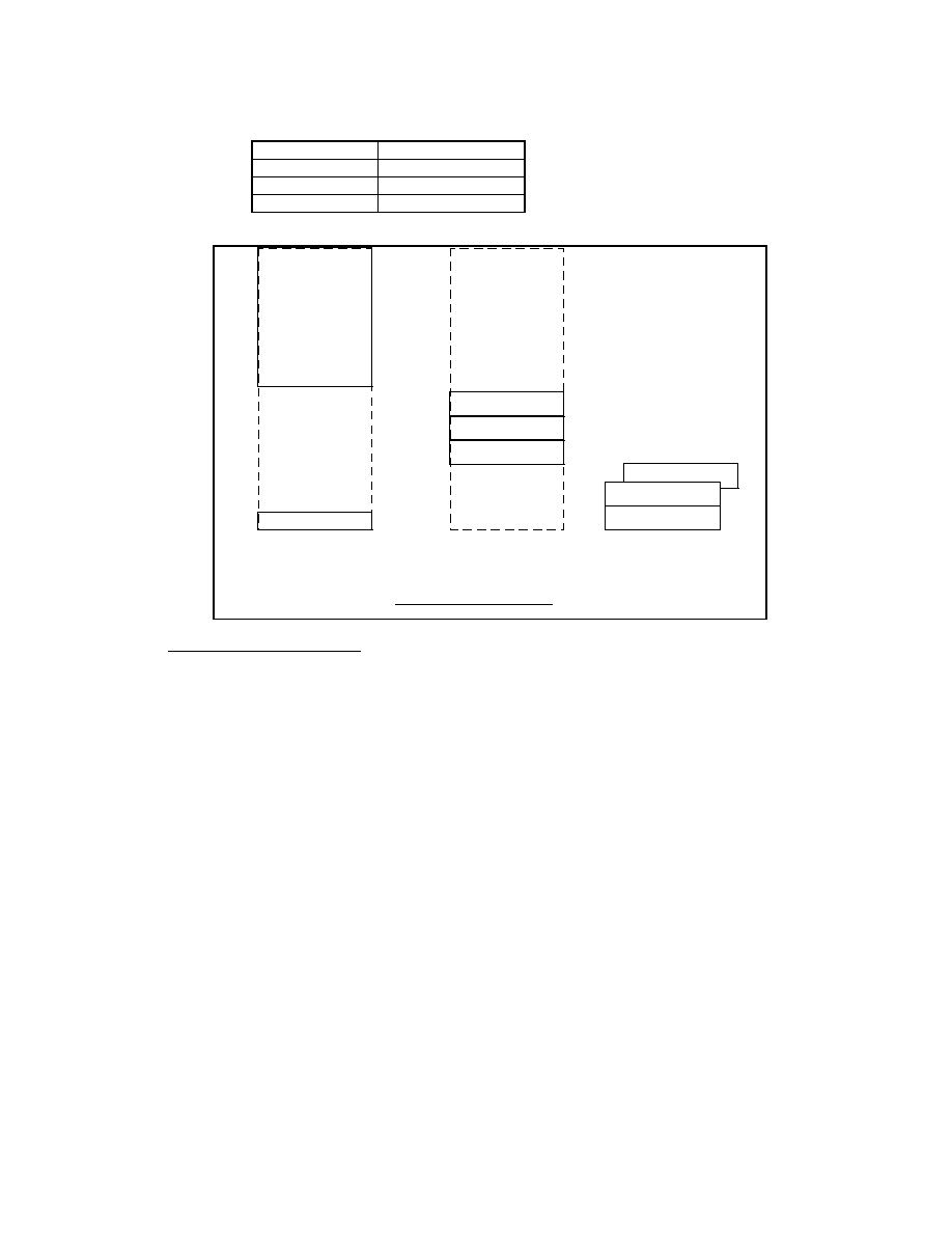
144
MMC bit = 0
When the MMC bit is low (VCC1 POR default) a hard coded long jump LJMP to 8000h is encoded at
addresses 00h through 02h and a 256 byte scratch RAM is located at external addresses 7D00-
7DFF. The encoding for the hard coded Long Jump is is shown in the following table.
8051 Address
Encoding
00h
02h
01h
80h
02h
00h
Table : Hard Coded LJMP to 8000h.
Program Memory
Data Memory
External
Internal
SFR (Direct Only)
Direct and Indirect
Indirect Only
00h
80h
7D00h
7E00h
7F00h
7FFFh
M/M Registers
RAM
Scratch RAM
8000h
FFFFh
nEA = 1, Reg MMC bit = 0
Hard Coded Internal
00h
02h
32K
External
FFh
80h
FFh
Instructions to access memory
MOV
: Internal RAM/Registers.
MOVC : Program ROM from 8000h through FFFFh
MOVX : External RAM from 7D00h through 7FFFh -AND-
External ROM from 8000h through FFFFh. (allows flashing of ROM).

145
MMC bit = 1
When the MMC bit is high the scratch RAM at 7D00h-7DFFh is disabled and now becomes the
executable internal scratch ROM at address locations 00h-0FFh. The hard coded LJMP to 8000h is
overridden by the scratch ROM.
Program Memory
Data Memory
External
Internal
SFR (Direct Only)
Direct and Indirect
Indirect Only
00h
80h
7D00h
7E00h
7F00h
7FFFh
M/M Registers
RAM
Scratch ROM
Internal
8000h
FFFFh
nEA = 1, MMC bit = 1
00h
FFh
32K
External
FFh
80h
FFh
Instructions to access memory
MOV
: Internal RAM/Registers.
MOVC : Program ROM from 8000h through FFFFh called from 00h-0FFh or from 8000h-0FFFFh.
Program ROM from 00h through 0FFh called from 00h-0FFh only.
MOVX : External RAM from 7E00h through 7FFFh -AND-
External ROM from 8000h through FFFFh. (allows flashing of ROM).

146
8051 Control Registers
Internal Special Function Registers (SFRs)
Table 53 is a map of the on-chip Special Function Register (SFR) space. The FDC37C957FR
provides all standard 80C51 SFRs (see the "Hardware Description of the 8051 and 8052 and 80C51"
in the 8-Bit Embedded Controller Handbook).
Table 53 - SFR Memory MAP
F8H
MSIZ
FFH
F0H
B*
F7H
E8H
EFH
E0H
ACC*
E7H
D8H
DFH
D0H
PSW*
D7H
C8H
CFH
C0H
C7H
B8H
IP*
BFH
B0H
P3*
B7H
A8H
IE*
AFH
A0H
P2*
A7H
98H
SCON*
SBUF
9FH
90H
P1*
97H
88H
TCON*
TMOD
TL0
TL1
TH0
TH1
8FH
80H
P0*
SP
DPL
DPH
Res
Res
Res
PCON
87H
First Column = Starting Address
Last column = Ending Address
*=Bit-addressable register
Res = Reserved for test
Port 0:
Full SFR, can be used for external memory access (but this corrupts the values in the SFR. ) Can
not sample any pins when reading the SFR.
Port 1:
Does not exist.
Port 2:
Full SFR, can be used to supply the high address byte for internal, external (MOVX) access to the
memory mapped registers or the flash registers.
Port 3: Does not exist.

147
External Memory Mapped Control Registers (MMCRs)
Table 54 describes the complete set of on-chip memory-mapped registers accessed by the 8051.
The internal memory mapped registers can be accessed by the following types of instructions.
1.
movx
A,@DPTR
2.
movx
@DPTR,A
3.
mov
P2,#7FH
movx
A,@Rx (R0 or R1 only)
4.
mov
P2,#7FH
movx
@Rx,A (R0 or R1 only)
ISAxxh = system ISA I/O address
IDXxxh = Open Mode Index Addressable Registers, See Configuration Section of this specification.
8051 Addresses = on-chip external Memory Mapped Register locations
Table 54 - 8051 On-Chip External Memory Mapped Registers
Sys.
index
Sys.
R/W
8051
address
(7F00+)
8051
R/W
Power
Source
VCC1
POR
VCC2
POR
Zero
Wait
State
(8)
Notes
See
Page #
Host I/F Data
Reg [KBD
Data/
Command
Write Reg.]
ISA
60h
ISA
64h
W
F1h
R
VCC1
N/A
Y
(1,7)
179
Host I/F Data
Reg
[KBD Data
Read Reg.]
ISA
60h
R
F1h
W
VCC1
N/A
Y
179
Host I/F Status
Reg [KBD
Status Reg.]
ISA
64h
R
F2h
R/W
VCC1
00h
Y
(2,7)
180
RTC
Address 1
ISA
70h
R/W
------
N/A
VCC1
00h
222
RTC Data 1
ISA
71h
R/W
------
N/A
VCC1
N/A
222
RTC
Address 2
ISA
74h
R/W
------
N/A
VCC1
00h
222
RTC Data 2
ISA
76h
R/W
------
N/A
VCC1
N/A
222
HTIMER
------
N/A
F3h
R/W
VCC1
00h
177
Config Reg 0
------
N/A
F4h
R/W
VCC1
00h
153
RTCCNTRL
------
N/A
F5h
R/W
VCC1
80h
6
201
RTCADDRL
------
N/A
F6h
R/W
VCC1
00h
202
RTCDATAL
------
N/A
F7h
R/W
VCC1
00
202
RTCADDRH
------
N/A
F8h
R/W
VCC1
00h
202
RTCDATAH
------
N/A
F9h
R/W
VCC1
00h
202

148
Sys.
index
Sys.
R/W
8051
address
(7F00+)
8051
R/W
Power
Source
VCC1
POR
VCC2
POR
Zero
Wait
State
(8)
Notes
See
Page #
Aux Host Data
Reg [KBD
Data Read
Reg.]
ISA
60h
R
FAh
R/W
VCC1
N/A
Y
3
183
GATEA20
------
N/A
FBh
R/W
VCC1
01h
185
PCOBF
------
N/A
FDh
R/W
VCC1
00h
181
SETGA20L
------
N/A
FEh
W
VCC1
N/A
185
RSTGA20L
------
N/A
FFh
W
VCC1
N/A
185
Interrupt 0
source register
------
N/A
00h
R
VCC1
00h
159
Interrupt 0
mask register
------
N/A
01h
R/W
VCC1
00h
159
Interrupt 1
source register
------
N/A
02h
R
VCC1
00h
160
Interrupt 1
mask register
------
N/A
03h
R/W
VCC1
00h
160
Keyboard
Scan out
------
N/A
04h
W
VCC1
20h
189
Keyboard
Scan in
------
N/A
04h
R
VCC1
N/A
190
Device Rev
register
------
N/A
06h
R
VCC1
01h
152
Device ID
register
------
N/A
07h
R
VCC1
07h
152
System-to-
8051
Mailbox
register 0
IDX
82h
R/W
08h
RC
VCC1
00
Y
4
192
8051-to-
system
Mailbox
register 1
IDX
83h
RC
09h
R/W
VCC1
00
Y
5
192
Mailbox
register [2-F]
IDX
84h-
91h
R/W
0A-17h
R/W
VCC1
00h
Y
193
GPIO
Direction
register A
------
N/A
18h
R/W
VCC1
00h
208
GPIO Ouput
register A
------
N/A
19h
R/W
VCC1
00h
209
GPIO Input
register A
------
N/A
1Ah
R
VCC1
N/A
209
GPIO
Direction
register B
------
N/A
1Bh
R/W
VCC1
00h
209
GPIO Ouput
register B
------
N/A
1Ch
R/W
VCC1
00h
210

149
Sys.
index
Sys.
R/W
8051
address
(7F00+)
8051
R/W
Power
Source
VCC1
POR
VCC2
POR
Zero
Wait
State
(8)
Notes
See
Page #
GPIO Input
register B
------
N/A
1Dh
R
VCC1
N/A
210
GPIO
Direction
register C
------
N/A
1Eh
R/W
VCC1
00h
12
210
GPIO Ouput
register C
------
N/A
1Fh
R/W
VCC1
00h
12
211
GPIO Input
register C
------
N/A
20h
R
VCC1
N/A
211
LED register
------
N/A
21h
R/W
VCC1
00h
12
199
OUT
register D
------
N/A
22h
R/W
VCC1
FFh
12
211
OUT
register E
------
N/A
23h
R/W
VCC1
0Fh
12
212
IN register F
------
N/A
24h
R
VCC1
N/A
212
PWM0 register
IDX
92h
R/W
25h
R/W
VCC1
00h
Y
200
PWM1 register
IDX
93h
R/W
26h
R/W
VCC1
00h
Y
200
KSTP_CLK
------
N/A
27h
R/W
VCC1
10h
154
KMEM
------
N/A
29h
R/W
VCC1
00h
165
WAKEUP
Source 1
------
N/A
2Ah
R
VCC1
00h
175
WAKEUP
Source 2
------
N/A
2Bh
R
VCC1
00h
175
WAKEUP
mask 1
------
N/A
2Ch
R/W
VCC1
00h
176
WAKEUP
mask 2
------
N/A
2Dh
R/W
VCC1
00h
177
Multiplexing 3
register
------
N/A
30h
R/W
VCC1
00h
220
ACCESS.BUS
Control reg
------
N/A
31h
W
VCC1
00h
196/236
ACCESS.BUS
Status reg
------
N/A
31h
R
VCC1
81h
196/237
ACCESS.BUS
Own Address
reg
------
N/A
32h
R/W
VCC1
00h
196/239
ACCESS.BUS
Data reg
------
N/A
33h
R/W
VCC1
00h
197/240
ACCESS.BUS
Clock
------
N/A
34h
R/W
VCC1
00h
197/240
WAKEUP
Source 3
------
N/A
35h
R
VCC1
00h
176
WAKEUP
Mask 3
------
N/A
36h
R/W
VCC1
FFh
177

150
Sys.
index
Sys.
R/W
8051
address
(7F00+)
8051
R/W
Power
Source
VCC1
POR
VCC2
POR
Zero
Wait
State
(8)
Notes
See
Page #
WDT
Control/Status
------
N/A
37h
R/W
VCC1
00h
162
TWD Timer
------
N/A
38h
R/W
VCC1
FFh
162
PP Status Reg
N/A
3Ah
R/W
VCC2
00h
9
204
PP Control
Reg
------
N/A
3Bh
R/W
VCC2
00h
205
PP Data Reg
------
N/A
3Ch
R/W
VCC2
00h
205
Multiplexing 1
register
------
N/A
3Dh
R/W
VCC1
00h
213
Output Enable
register
3Eh
R/W
VCC1
see
note
see
note
11
156
DISABLE
register
------
N/A
3Fh
R/W
VCC1
00h
155
Multiplexing 2
register
------
N/A
40h
R/W
VCC1
00h
216
PS/2 port1
Control
register
N/A
41h
R/W
VCC2
00h
194/242
PS/2 port1
status register
N/A
42h
R
VCC2
00h
194/243
PS/2 port1
Error Status
Register
N/A
43h
R
VCC2
00h
195/244
PS/2 port1
Transmit Reg
N/A
44h
W
VCC2
00h
195/245
PS/2 port1
Receive Reg
N/A
45h
R
VCC2
00h
195/245
RESERVED -
SMC
------
N/A
46h-48h
--
-------
----
----
_ _ _
PS/2 port2
Control
register
------
N/A
49h
R/W
VCC2
00h
194/242
PS/2 port2
status register
------
N/A
4Ah
R
VCC2
00h
194/243
PS/2
port2Error
Status
Register
------
N/A
4Bh
R
VCC2
00h
195/244
PS/2 port2
Transmit Reg
------
N/A
4Ch
W
VCC2
00h
195/245
PS/2 port2
Receive Reg
------
N/A
4Dh
R
VCC2
00h
195/245
RESERVED -
SMC
------
N/A
4Eh-4Fh
--
-------
----
----
_ _ _

151
Sys.
index
Sys.
R/W
8051
address
(7F00+)
8051
R/W
Power
Source
VCC1
POR
VCC2
POR
Zero
Wait
State
(8)
Notes
See
Page #
256 bytes of
RAM
------
N/A
7E00-
7EFFh
R/W
VCC1
_ _ _
Notes
1. Although the Input and Output Data registers are physically separate, they share address 7FF1H.
2. The ORION CPU cannot write to some bits of the Status register.
3. Writing to the Auxiliary Output Data Register, loads the Output data register and can set
the AUXOBF1 output if enabled. This does not set the PCOBF output.
4. Interrupt is cleared when read by the 8051
5. Interrupt is cleared when read by the host
6. See RTC control Register Definition
7. When accessed for a read or write by the System the registers marked with a "Y" will drive the
Zero wait state pin active.
8. Bit 0 is the only writable or resetable bit in this register.
9. When IRESET_OUT is cleared (written from "1" to"0") 8051STP_CLK bit D0 as well as HMEM
bits D1 and D0 are all set to "1".
10. VCC1 POR = 00000X10b, VCC2 POR = 00000X1Xb where X is not affected by VCC2 POR, but
is left at the current value.
11. These registers are reset 500us to 1ms following the condition that BOTH VCC2 is valid and
PWRGD is asserted given that the RTC is in normal mode and the VRT bit is set (refer to the
RTC section). If the RTC is not in normal mode and/or the VRT bit is not set then these registers
are reset within 10us following the condition that BOTH VCC2 is valid and PWRGD is asserted.

152
8051 Configuration/Control Memory Mapped Registers
Device Rev register
By reading this register, 8051 firmware can confirm the device revision that it is running on.
Host
N/A
8051
0x7F06 (R)
Power
VCC1
Default
0x01
D7-D0
8051 R
R
Bit description
Hard-wired to 01h
Device ID register
By reading this register, 8051 firmware can determine which device it is running on.
Host
N/A
8051
0x7F07 (R)
Power
VCC1
Default
0x07
D7-D0
8051 R
R
Bit description
Hard-wired to 07h.

153
Configuration Register 0
Host
N/A
8051
0x7FF4
Power
VCC1
Default
0x00
Table 55 - Configuration Register 0
D7
D6
D5
D4
D3
D2
D1
D0
AUXH
0
OBFEN
0
MMC
PCOBFEN
SAEN
SLEEPFLAG
AUXH
Aux in Hardware; When high, AUXOBF of the status register is set in hardware by a
write to 7FFAh. When low, AUXOBF of the status register is a user defined bit
(UD) and R/W.
OBFEN
when set PCOBF is gated onto KIRQ and AUXOBF1 is gated onto MIRQ. When
low, KIRQ and MIRQ are driven low. Software should not change this bit when OBF
of the status register is equal to 1.
MMC
Memory Map Control Bit : When MMC=0, a 256 Byte Scratch RAM area at 7D00h
is available to the 8051. When MMC=1 the Scratch RAM at 7D00h-7DFFh
becomes scratch ROM at 00h--FFh.
PCOBFEN
When high, PCOBF reflects whatever value was written to the PCOBF firmware
latch assigned to 7FFDH. When low, PCOBF reflects the status of writes to 7FF1H
(the output data register).
SAEN
Is the software-assist enable. When set to `1' SAEN allow control of the GATEA20
signal via firmware. If SAEN is reset to `0', GATEA20 corresponds to either the last
host-initiated control of GATEA20 or the firmware write to 7FFEh or 7FFFh.
SLEEPFLAG
If SLEEPFLAG="0" when PCON bit-0 is set, the 8051 enters "IDLE" mode, whereas
if SLEEPFLAG="1" when PCON bit-0 is set the 8051enters "SLEEP" mode. This
bit is cleared by the occurrence of any wake-up events and on VCC1 POR.

154
KSTP_CLK Register
Host
N/A
8051
0x7F27
Power
VCC1
Default
0x10
D7
D6
D5
D4
D3
D2
D1
D0
KBCLK1
KBCLK0
KBCLK/ROSC
ROSCEN
STP_CNT[3:0]
Note: ROSC refers to the ring oscillator.
STP_CNT[x] This defines the number of machine cycles from when the internal IRESET_OUT bit is
cleared until the external RESET_OUT pin goes inactive low (deasserts) .
ROSCEN This bit reflects the state of the ring oscillator clock at all times. The 8051 can write this bit
to start or stop the ring oscillator. Other hardware events can also start or stop this clock.
=1 turn on ring oscillator
=0 turn off ring oscillator
This bit is reset when the 8051 goes into "SLEEP" mode and is set when the 8051 first
wakes up from "SLEEP" mode.
KBCLK/ROSC This bit is used to control the clock source for the 8051.
1 = 8051 clock source is KBCLK
0 = 8051 clock source is ring oscillator.
This bit is reset when the 8051 just wakes up from the "SLEEP" mode
KBCLK1
KBCLK0
0
0
stop KBCLK (default)
0
1
KBCLK = 12 MHz
1
0
KBCLK = 14. 318 MHz
1
1
KBCLK = 16 MHz

155
DISABLE register
Host
N/A
8051
0x7F3F
Power
VCC1
Default
0x00
If `0', these bits override the enable bits in the Configuration registers.
D7
D6
D5
D4
D3
D2
D1
D0
8051
R/W
R/W
R/W
R/W
R/W
R/W
R/W
R/W
R/W
System
R/W
N/A
N/A
N/A
N/A
N/A
N/A
N/A
N/A
Parallel
Port
1 =
Enable
0 =
disable
serial
port
1 =
Enable
0 =
disable
IR port
1 =
Enable
0 =
disable
floppy
port
1 =
Enable
0 =
disable
User
Defined
system
flash
interface
1 =
Enable
0 =
disable
Note 1
Re-
served
Re-
served
Note 1: If D2=0, then the FLASH is write protected from the system. The system can still read the FLASH

156
Output enable register
Host
N/A
8051
0x7F3E
Power
VCC1
Default
00000X10b on VCC1 POR
00000X1Xb on VCC2 POR
Output Enable Register VCC1 POR = 0x00000X10, VCC2 POR = 00000X1Xb where X means the
bit holds its setting preceding VCC2 POR.
D7-D4
D3
D2
D1
D0
8051 AR
R/W
R/W
R
R/W
R/W
Reserved
0
iRESET_
OVRD
Power_Good
iRESET_OUT
32KHz
Output
AR= Access Rights
IRESET_OUT Definition:
When POWERGOOD=1, IRESET_OUT is controlled by the 8051.
When POWERGOOD=0, IRESET_OUT is forced high (within 100nsec) and latched. The
RESET_OUT pjn is not driven until VCC2 is applied. IRESET_OUT cannot be cleared by the 8051
until POWERGOOD=1.
iRESET_OVRD :
iRESET Override - when cleared the iRESET_OUT bit functions as described above (i.e., as on the
current Orion devices). When set, iRESET_OUT is given direct control over the internal reset and
perhaps the RESET_OUT and nRESET_OUT pins without requiring the STOP_CLK counter or
affecting the 8051STP_CLK bit or the HMEM register. In the override mode, setting iRESET_OUT
may or may not drive RESET_OUT high and clearing iRESET_OUT may or may not drive
RESET_OUT low.
The RESET_OUT Override function allows the 8051 to take the rest of the Orion FR chip (SIO) out of
reset without giving up control (i.e., without stopping its clock and giving the flash interface to the
Host).
On the current Orion device, RESET_OUT is driven low by this sequence of events (refer to
FIGURE
4 - TYPICAL SYSTEM RESET SEQUENCE for more infomation :
1) 8051 sets STP_CNT to a non-zero value
2) 8051 clears iRESET_OUT bit, causing...
a) 8051STP_CLK bit-0 to get set.
b) HMEM[7:0] to get set to 0x03
c) and STOP Counter to start decrementing
3) When STP_CNT reaches 0 the RESET_OUT pin deasserts (goes low) at which point the
8051's clock stops and the Host owns the Flash interface.

157
In addition to the above sequence, the FDC37C957FR provides a means for the 8051 to directly
control the state of the Super I/O block's internal reset. The FDC37C957FR provides a means for the
8051 to drive low or toggle the chip's internal reset without stopping the 8051 clock or giving the Flash
interface to the Host.
8051 Interrupts
The FDC37C957FR provides the five standard 8051 interrupts (Group 0) plus an additional T5INT
interrupt which is located at the vector address for Timer 2 which is standard on the 8052 standard
micro-controller. Table 56 describes the interrupts.
The Group 0 interrupts use the standard 8051 interrupt enable and priority structures. Each interrupt
is individually enabled or disabled by setting or clearing a bit in the interrupt Enable (IE) register (SFR
location A8H). Each interrupt is programmed to one of two priority levels by setting or clearing a bit in
the interrupt Priority (IP) register (SFR location B8H). See the "Hardware Description of the 8051,
8052, and 80C51" in the 8-Bit Embedded Controller Handbook for more details.
Group 0 interrupts (which HAVE MODIFIED SOURCES FROM the standard 80C51 interrupts) are
configurable as either level-or-edge sensitive. Consult the 8-Bit Embedded Controller Handbook for a
full description.
Table 56 - Interrupt Sources
INTERRUPT
DESCRIPTION
VECTOR
ADDRESS
POLLING
ORDER
ACTIVE
Group 0
INT0
Interrupt INT0
03H
0 (IE0)
L/E
T0INT
Timer 0 Interrupt
0BH
1 (IE1)
INT1
Interrupt INT1
13H
2 (IE2)
L/E
T1INT
Timer 1 Interrupt
1BH
3 (IE3)
Serial Port
Serial Port Interrupt
23H
4 (IE4)
E
T5INT
T5 Interrupt (1)
2BH
5 (IE5)
Note: L = Level-sensitive, E = Edge-sensitive
Note (1): the T5 interrupt, if enabled, is generated as a result of the occurrence of any un-
masked wake-up event.

158
Interrupt Enable register (IE):
This register is based on the standard 8051 IE register. It has been modified to add a definition for bit
D5.
D7
D6
D5
D4
D3
D2
D1
D0
Default
0
0
0
0
0
0
0
0
Bit Def
EA
Reserve
d
T5INT
interrupt
enable
bit
RI+TI
8051
Serial
Port
interrupt
enable bit
TF1
Timer 1
interrupt
enable bit
INT1
External
Interrupt 1
enable bit
TF0
Timer 0
interrupt
enable bit
INT0
External
interrupt 0
enable bit
Interrupt Priority register (IP):
This register is based on the standard 8051 IP register. It has been modified to add a definition for bit
D5.
D7-D5
D5
D4
D3
D2
D1
D0
Default
0
0
0
0
0
0
0
Bit Def
Reserve
d
T5INT
interrupt
priority
bit
8051
Serial
Port
interrupt
priority
bit
Timer 1
interrupt
priority
bit
External
Interrupt
1 priority
bit
Timer 0
interrupt
priority
bit
External
interrupt
0 priority
bit
Interrupt Polling Sequence
When two or more interrupts with the same priority level become active during the same machine
cycle, the chip's internal polling sequence determines the service order. If all six interrupts are set to
the same priority level, and all interrupts become active during the same machine cycle, the 8051
services the interrupts in the order shown in Table 56.
Additional Interrupt sources
Inside the FDC37C957FR, interrupt events from various sources are able to generate either an INT0
or INT1 8051 interrupt. The 8051 firmware masks these interrupt sources by writings "1's" into the
8051 INTO or INT1 Mask Registers and enables these interrupts by writing "0's" into these mask
registers. The 8051 can determine the source of the INT0 or INT1 interrupt by reading the 8051 INTO
or INT1 Source Register.
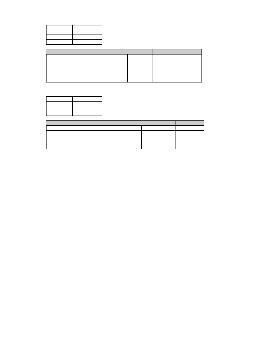
159
8051 INT0 source register
Host
N/A
8051
0x7F00 (R)
Power
VCC1
Default
0x00
D7-D4
D3
D2
D1
D0
8051 R/W
R
R
R
R
R
Bit Description
Reserved
1=MSB
Receive
Data
Changed
1=
WK_EE4
transition
(both
edges)
1 =
WK_EE2
transition
(both
edges)
1 =
WK_EE3
transition
(both
edges)
Note: this register is cleared on a read.
8051 INT0 mask register
Host
N/A
8051
0x7F01
Power
VCC1
Default
0x00
D7-D4
D3
D2
D1
D0
8051 R/W
R/W
R/W
R/W
R/W
R/W
Bit Def
Reserve
d
1=mask
MSB
1 = mask
WK_EE4
(Edge)
1 = mask
WK_EE2
transition
interrupt
1 = mask
WK_EE3
transition
interrupt
When enabled, INT0 is generated on either positive or negative-going edge of WK_EE4 [ERDY].

160
8051 INT1 source register
Host
N/A
8051
0x7F02 (R)
Power
VCC1
Default
0x00
D7
D6
D5
D4
D3
D2
D1
D0
8051
R/W
R
R
R
R
R
R
R
R
Bit Des.
1=
IBF
Note 1
1 =
keyboard
scan-in
line.
Note 2
1=
PS/2 port2
Flag
(L to H)
1=
PS/2
port1
flag
(L to H)
1=
GPIO3
(Both
Edges)
1=Acc-
ess Bus
Note 4
1=
system
writes to
mailbox
register
0
Note 5
1= A
Wake-
up
event is
active
Bits D0, D2-D6 are cleared by a read. To re-enable these IRQ's you must reset the interrupting
condition! (i.e., all active interrupts must be serviced after reading this register).
Note 1: The IBF interrupt bit is set when the host writes to the KBD Data/Command Write Regiter
and cleared when the 8051 reads the data from that register.
Note 2: Bit D6 is latched on a high to low transition. of any of the keyboard scan lines.
Note 3: When enabled, INT1 is generated on either positive or negative-going edge of GPIO3.
Note 4: An Access Bus IRQ is active.
Note 5: This bit is set when the system writes to mailbox register 0. This bit is cleared by a read
of the mailbox 0 register
8051 INT1 mask register
Host
N/A
8051
0x7F03
Power
VCC1
Default
0x00
D7
D6
D5
D4
D3
D2
D1
D0
8051
R/W
R/W
R/W
R/W
R/W
R/W
R/W
R/W
R/W
Bit
Def
1=
mask
IBF
1 = mask
the
keyboard
matrix
scan flag
1 =
mask
PS/2
port2
Flag
1 = mask
PS/2
port1 Flag
1 =
mask
GPIO3
1=
mask
Access
Bus
1 = mask
system-to-
8051
mailbox
register
interrupt
1 =
mask
Wake-
up
events

161
Watch Dog Timer
WDT Operation
When enabled, the Watch Dog Timer (WDT) circuit will generate a system reset if the user program
fails to reload the watchdog timer (TWD) within a specified length of time known as the `watchdog
interval'.
The WDT consists of an 8-bit timer (TWD) with a 9-bit prescaler. The prescaler is fed with 32KHz
which always runs, even if the 8051 is in SLEEP state. The 8-bit TWD timer is decremented every
(1/32KHz) *512 seconds or 16.0 ms. Thus, the watchdog interval is programmable between 16ms
and 4.08 seconds on 16ms intervals.
WDT Action
If the 8 bit timer (TWD) underflows, a VCC1 POR is generated
8051 in idle mode - WDT will be active if enabled. When the TWD timer underflows in idle mode, the
8051 will be reset. It is up to the firmware engineer to design code that uses a timer to generate an
interrupt that will exit idle mode and re-initialize the TWD timer and then put the 8051 back into idle
mode.
8051 in sleep mode - if enabled, the WDT is active since it is running off of the 32KHz clock.
Therefore, if the WDT is enabled the 8051 should never remain in the SLEEP state for more than 4
seconds.
WDT Activation
Upon VCC1 POR the Watch Dog Timer powers up inactive. The Watch Dog Timer shall be activated
when the WDT enable bit (WDT CONTROL bit D1) is set by 8051 firmware. The WDT may be
disabled under software control through a specific sequence. Software can clear the SDT enable bit
by :
1)
Setting the WLE-WDT Load enable bit in the WDT Control/Status Register
2)
Writing 00h to the TWD Timer Register (this causes the WDT Enable and the
WLE_WDT Load Enable bits to each reset to 0).
Once the WDT has been activated, this sequence must be executed in order to disable watchdog
operation via software control. Note: Since a VCC1 POR will reset the WDT enable bit, the WDT
must be re-enabled after each occurrence.
162
WDT Reset Mechanism
The watchdog timer (TWD) must be reloaded within periods that are shorter than the programmed
watchdog interval; otherwise the TWD will underflow and a VCC1 POR will be generated. It is the
responsibility of the user program to continually execute sections of code which reload the 8-bit timer
(TWD).
The WDT is reloaded in two stages in order to prevent erroneous software from reloading the
watchdog. First WDT CONTROL bit-D0 (WLE-WDT Load Enable) must be set. Then the TWD may
be loaded. When TWD is loaded WLE is automatically reset. TWD can not be loaded when WLE is
reset. Since the TWD timer is a down counter , a reload value of 01h results in the minimum WDT
interval (16ms) and a reload value of 0FFh results in the maximum WDT interval (4.08 seconds).
Loading 00h into the TWD disables the WDT and clears the WDT Enable bit. Note, the 9-bit
prescaler is initialized whenever the TWD timer is loaded.
WDT Memory Mapped Registers
TWD: Put at Location 7F38 (Default = 0xFF, on VCC1 POR).
D7
D6
D5
D4
D3
D2
D1
D0
8051 R/W
R/W
System R/W
N/A
Bit Def
TWD Timer
WDT CONTROL/STATUS: Put at Location 7F37. (Default = 0x00, on VCC1 POR).
D7-D2
D1
D0
8051 R/W
R
R/W
R/W
System R/W
N/A
N/A
N/A
Bit Def
Reserved
WDT Enable
WLE-WDT Load Enable
WLE :
Watchdog Load Enable bit must be set to enable writing to the TWD Timer register. This
bit is automatically reset when the 8051 writes to the TWD register. If this bit is
reset, writes to the TWD register are ignored.
WDT Enable :
The WDT enable bit must be set by 8051 firmware to enable or start the Watch Dog
Timer. A VCC1 POR or the above described software sequence will reset this bit.

163
Shared Flash Interface
A 256KB Flash Device (i.e., 28F020) is recommended to store the program code for the 8051
(Keyboard BIOS + ) and the system BIOS. The FLASH memory can be accessed from the system in
blocks of 64KB or from the 8051 in blocks of 32KB. The procedure to access the FLASH memory is
described in the "Host Flash Access" section.
Flash Interface Diagram
Access to the Flash Memory is multiplexed inside of the FDC37C957FR. The Host CPU only has
access to the Flash when (nRESET_OUT is not asserted and the 8051 STP_CLK bit-0 is set).
Please refer to the Timing section of this specification for details on this interface.
ORION
256K x 8
FLASH
LATCH
AD[7:0]
R
O
M
_
C
S
#
I
S
A
B
U
S
ADDR[17:8]
KBRD#
KBWR#
ALE
HOST CPU
nCE
FIGURE 5 - FLASH INTERFACE DIAGRAM
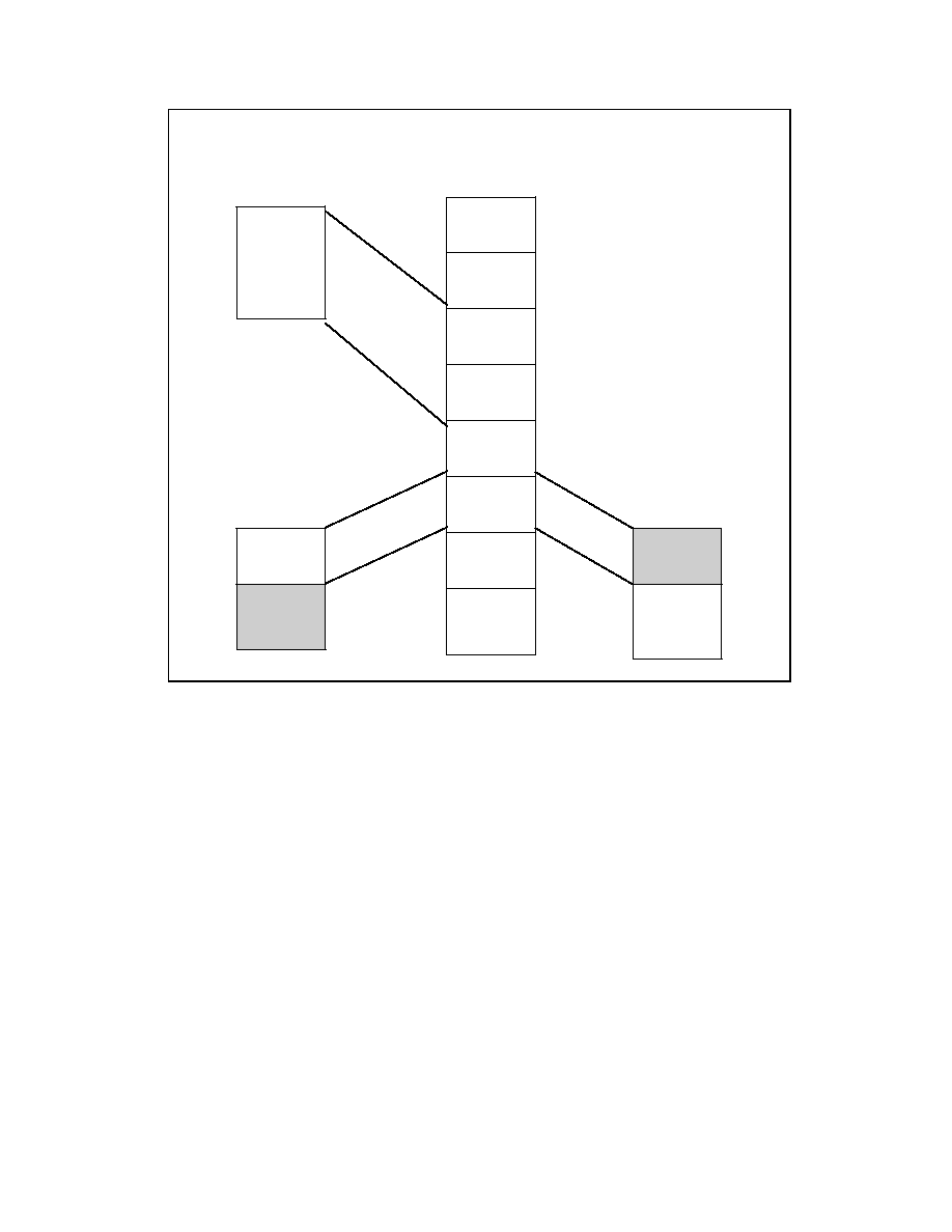
164
System Flash Access Map
64K
8051
ROM
256K
FLASH
ROM
0
64K
Host
Interface
64K
8051
External
RAM
0
8000
FFFF
8000
FFFF
8x
32K Blocks
0
FFFF
Internal
Registers
Same as
0-7FFF
FIGURE 6 - 8051 MODE 2

165
Keyboard BIOS (KMEM)
KMEM Register
Host
N/A
8051
0x7F29
Power
VCC1
Default
0x00
D7-D3
D2
D1
D0
8051 R/W
R/W
R/W
R/W
R/W
System R/W
N/A
N/A
N/A
N/A
Bit Def
00 on read
A[17]
A[16]
A[15]
The 8051 uses this register to access the Flash ROM in a 32K window. The 8051 is only barred from
accessing the Flash when 8051STP_CLK bit D0 =1 and RESET_OUT=low or deasserted.
KMEM
17
16
15
Flash memory
range
0
0
0
000- 7FFF
0
0
1
8000- FFFF
0
1
0
10000-17FFF
0
1
1
18000-1FFFF
1
0
0
20000-27FFF
1
0
1
28000-2FFFF
1
1
0
30000-37FFF
1
1
1
38000-3FFFF

166
System BIOS (HMEM)
HMEM Register
Host
IDX 0x95
8051
N/A
Power
VCC1
Default
VCC1 POR =
0x03
VCC2 POR =
0x03
D7-D2
D1
D0
8051 R/W
R
R
R
System R/W
R/W
R/W
R/W
Bit Def
0
A[17]
A[16]
The System uses this register to select a 64K window for access from the 256K Flash ROM. The
Host may access the Flash when RESET_OUT pin is de-asserted and 8051STP_CLK bit D0 = 1.
Host Flash Access
The FDC37C957FR has a special shared Flash ROM interface. The 8051 can be stopped to allow
the Host CPU to access the flash ROM after a special handshake sequence is followed.
HOST INITIATED FLASH ACCESS:
To access the FLASH memory, the 8051 must first be placed into idle mode, and then the 8051 clock
must be stopped. Host Flash Read and Writes occur when the nROMCS pin is asserted along with
nMEMRD or nMEMWR. The register bit "8051_STPCLK" needs to be set by the host to make the
8051 clock stop. The 8051 clock is only stopped when 8051STP_CLK=1 and when RESET_OUT pin
= low. Address bits A[15:0] are supplied by SA[15:0], address bits A[17:16] are supplied by
configuration register HMEM. For Flash access, these address lines and bits are qualified (selected)
by 8051STP_CLK=1, and the RESET_OUT pin = low (RESET_OUT is driven by the 8051).,
8051STP_CLK is set to "1" and HMEM is set to 03h (effectively resulting in A[17:16] initializing as
"11" whenever the 8051 clears the IRESET_OUT bit from "1" to "0". This allows the system to
execute from the upper 64K of the FLASH memory at boot time. To access the other portions of the
FLASH memory, the system software must first change the values of HMEM[1:0] register to control
address lines A[17:16]. The access to the FLASH memory uses nFWR for a write and nFRD for a
read.

167
The Host, wishing to access
Flash memory, issues a user
defined command to put the
8051into idle mode.
System fully powered
up and running.
R E S E T _ O U T = l o w , 8 0 5 1 S T P _ C L K = 0 .
8051 owns Flash interface,
Running Keyboard Code.
8051goes into idle mode
When done using Flash,
the Host resets
8051STP_CLK bit
8051 Timer
I R Q ?
Y
N
The Host sets
8051STP_CLK = 1;
combined with
RESET_OUT = low, this
causes 8051 clock to stop.
Host now owns Flash
nterface.
8051 wakes up from idle
mode and starts executing
from where it left off.
(Note)
Figure 7 - DYNAMIC SHARING OF FLASH INTERFACE BETWEEN HOST AND 8051

168
8051 STP_CLK Register
Host
IDX 0x94
8051
N/A
Power
VCC1
Default
0x00
D7
D6
D5-D1
D0
IDLE
HOST_
FLASH
Reserved, set to 0
0=8051 Clock can run
1=8051 clock stop
Note : When bit D0=1 the 8051's clock is not stopped unless the RESET_OUT pin is also de-
asserted at which point the Host has access to the Flash Memory.
Note : Only bit D0 is R/W, bits[7:1] are Read only.
IDLE : 0 = 8051 not in idle mode
1= 8051 in idle mode
HOST_FLASH : 0 = Host does not have access to Flash, in use by 8051
1 = Host has access to Flash
8051 System Power Management
The 80C51 core provides support for two further power-saving modes, available when inactive:
"IDEL" mode, typically entered between keystrokes; and "SLEEP" mode, entered upon command
from the host. The 8051 is wake-able from "SLEEP" mode through a set of external and internal
events called Wake-Up events. The events are listed in Table 57 - System Wake-up Events. When
exiting the "SLEEP" mode, the 8051 will continue executing code from where it left off when put into
"SLEEP" with no changes to the SFR and pins.
The FDC37C957FR is fully static and will pick-up from where it left off in the event of a wake-up
event.
Idle Mode
Entering IDLE mode:
Idle mode is initiated by an instruction that sets the PCON.0 bit (SFR address 87H) in the keyboard.
In idle mode, the internal clock signal to the keyboard CPU is gated off, but not to the Interrupt Timer
and Serial Port functions. The CPU status is preserved in its entirety: the Stack Pointer, Program
Counter, Program Status Word, Accumulator, and all other registers maintain their data. The port
pins hold the logical levels they had when Idle mode was activated.

169
System fully powered
up and running.
RESET_OUT=low, 8051STP_CLK=0.
8051 owns Flash interface,
Running Keyboard Code.
8051 now in idle mode,
8051 clock running.
The Host either issues a user
defined command to put the
8051into idle mode, or the
8051 code determines that
the 8051 should enter
idle Mode.
SLEEPFLAG = 0
PCON.0 = 1
ENTERING IDLE MODE

170
un-masked
8051 IRQ ?
N
8051 returns to executing
from where it left off prior to
entering idle mode.
(Note)
8051 in idle mode,
8051 clock running.
Note: In order to leave idle mode the
8051 must receive an interrupt, typically
a software timer interrupt will be used.
EXITING IDLE MODE DUE TO IRQ.
Y
8051 leaves idle mode,
executes IRQ service routine
code and executes an IRET
when done.
Exiting IDLE mode
There are two ways to terminate Idle mode. First, activation of any enabled interrupt will cause the
PCON.0 bit to be cleared by hardware. The interrupt will be serviced and, following the RETI, the
CPU will resume operation by executing the instruction following the one that put the CPU into Idle
mode.
The second way to terminate the Idle mode is with a VCC1 POR. Note that a VCC1 POR will clear
the registers. The CPU will not resume program execution from where it left off.

171
Sleep Mode
"SLEEP" mode sequence
To enter "SLEEP" mode, the 8051:
1)
turns on the ring oscillator (KSTP_CLK[4] = 1)
2)
switches the clock source (KSTP_CLK[5] = 0)
3)
turns off the clock chip (or the whole system power, VCC2)
4)
masks all interrupts except for T5INT
5)
sets SLEEPFLAG = 1
6)
sets PCON.0 = 1
7)
the ring oscillator will be automatically turned off
8)
the 8051 goes into "SLEEP" mode
"SLEEP" mode is initiated by a user defined command of event to the 8051. . When the CPU enters
"SLEEP" mode, all internal clocks, including the core clocks, are turned off. If an external crystal is
used, the internal oscillator is turned off. RAM contents are preserved.
Design Note:
In this mode, the FDC, UART1, UART2 and parallel port are powered off if VCC2 is
removed, but the RTC and 8051 are in powerdown (sleep) mode, the chip must consume
less than 20uA, and all wake-up pins must still be active.
Exiting "SLEEP" Mode:
When the 8051 is in "SLEEP" mode, all of the clocks are stopped and the 8051 is waiting for
an unmasked wake-up event. When the wake-up event occurs, the ring oscillator is started,
once this has stabilized, the 8051 starts executing from where it stopped in the "SLEEP"
Mode Sequence. Once running, the 8051 can access all of the registers that are on VCC1
and if VCC2 is at 5V it can access all of the registers on VCC2. The 8051 running from the
ring oscillator clock source can turn on the clock chip, switch its clock source to 16 Mhz and
then turns off the ring oscillator clock source.

172
System fully powered
up and running.
RESET_OUT=low, 8051STP_CLK=0.
8051 owns Flash interface,
Running Keyboard Code.
8051 now in
"SLEEP" mode,
8051clock stopped.
The Host either issues a user
defined command to put the
8051into "SLEEP" mode, or
the 8051 code determines
that the 8051 should enter
"SLEEP" Mode.
SLEEPFLAG = 1
PCON.0 = 1
ENTERING "SLEEP" MODE
8051 switches its clk source
to the ring oscillator.
8051 masks all interrupts
except for T5INT.
ring oscillator first gated off
from 8051, then turned off.
The 8051 may/may not turn
off VCC2 to rest of system.
173
Wake Up Events :
RTCAlarm,
Power button,
Ring Indicator,
etc.
8051 in "SLEEP" mode.
RTC, 8051 and other VCC1
driven pins are active
un-masked
Wake-up
Event ?
N
Y
T5INT generated.
Turn on ring oscillator.
SLEEPFLAG = 0.
Once stabilized, the ring
oscillator is gated through to
the 8051.
The 8051 is now running in
idle mode and responds
immediately to T5INT.
8051 returns to executing
from where it left off prior to
entering "SLEEP" mode.
8051 leaves idle mode,
executes T5INT service
routine (disables T5INT) and
executes an IRET when
done.
EXITING SLEEP MODE

174
Wake-up Events
Table 57 - System Wake-up Events
PIN
WAKE-UP
EVENTS
LEVEL/EDGE
SENSITIVE
INTERNAL
OR
EXTERNAL
DESCRIPTION
nRI1, nRI2
nRI1, nRI2
Edge, high-to-
low
External
UART Ring
Indicator
nGPWKUP
nGPWKUP
Edge - high-to-
low
External
General purpose
wakeup source
WK_HL1
WK_HL1
Edge - high-to-
low
External
WK_HL2
WK_HL2
Edge - high-to-
low
External
AB_DAT
ACCESS.BUS
DATA going active
Leading Edge,
high-to-low
Internal
ACCESS.BUS
Interrupt
WK_HL3
WK_HL3
Edge, high-to-
low
External
WK_HL4
WK_HL4
Edge, high-to-
low
External
WK_HL5
WK_HL5
Edge, high-to-
low
External
WK_EE1
WK_EE1
Either edge
External
N/A
RTC_ALRM (1)
Leading Edge,
low-to-high
Internal
RTC alarm
N/A
HTIMER
Leading Edge,
low-to-high
Internal
Hibernation timer
WK_EE2
WK_EE2
Either edge
External
WK_EE3
WK_EE3
Either edge
External
WK_HL6
WK_HL6
Edge - high-to-
low
External
WK_EE4
WK_EE4
Either edge
external
N/A
(function of
KSI[7:0]
pins)
WK_ANYKEY
Edge
(High-to-Low)
Internal
Any Keyboard
Key pressed
GPIO8/COM
-RX
WK_HL7
[IR_WAKEUP]
Edge
(High-to-Low)
External
IR energy
detected on the
GPIO/COM-RX
Receive pin.
IRRX
WK_HL8
[IR_WAKEUP]
Edge
(High-to-Low)
External
IR energy
detected on the
RRRX Receive
pin.

175
Wakeup Source Register 1
Host
N/A
8051
0x7F2A (R)
Power
VCC1
Default
0x00
D7
D6
D5
D4
D3
D2
D1
D0
8051
R/W
R
R
R
R
R
R
R
R
Def
1 =
WK_
HL5
1 = WK_
HL2
occurs
1 =
WK_HL
1occurs
1 =
AB_DAT
ACCESS.
BUS
interrupt
occurs
1 =
WK_HL3
occurs
1 =
WK_HL4
occurs
1 =
WK_EE1
changed
(Note 1)
1 =
RTC_AL
RM
occurs
(Note 2)
Note : All the bits in this register are cleared on a read of this register.
Note 1: Input is going from low to high or from high to low (read the GPIO register to find out the
value of pin) ACCESS.BUS Interrupt -- When ACCESS.BUS=1, a start condition or other
event was detected on the ACCESS.BUS bus
Note 2: The RTC_ALRM Wake-up is an internally generated Low-to-High edge, produced when the
RTC time updates to match the Time Of Day (TOD) alarm setting. This edge will set bit D0
of Wake-up Source 1 Register. Bit D0 will remain set and will only be reset on a read of
Wake-up Source 1 Register. If the Wake-up source register is read before the clock has
updated (i.e., RTC still equals the TOD alarm) bit D0 is reset and stays reset until the next
occurrence of a RTC_ALRM Wake-up event.
Wakeup source register 2
Host
N/A
8051
0x7F2B (R)
Power
VCC1
Default
0x00
D7
D6
D5
D4
D3
D2
D1
D0
8051
R/W
R
R
R
R
R
R
R
R
Des.
1 =
UART_R
I2 occurs
1 =
UART_R
I1 occurs
1=
WK_
EE4
1 =
WK_EE2
transition
(both
edges)
1 =
WK_EE3
transition
(both
edges)
1 =
HTIMER
timeouts
1 =
WK_HL6
active
1=
nGPWKU
P is active
Note : All the bits in this register are cleared on a read of this register.
HTIMER Interrupt -- When HTIMER=1, the hibernation timer counted down to zero.

176
Wakeup Source Register 3
Host
N/A
8051
0x7F35 (R)
Power
VCC1
Default
0x00
D7
D6
D5
D4
D3
D2
D1
D0
8051
access
R
R
R
R
R
R
R
R
Host
access
N/A
N/A
N/A
N/A
N/A
N/A
N/A
N/A
Des-
cription
Reserve
d
0
Reserve
d
0
Reserve
d
0
Reserve
d
0
Reserve
d
0
1=
WK_
HL8
is active
1=
WK_
HL7
is active
1=
WK_
ANYKEY
is active
Note : All the bits in this register are cleared on a read of this register.
Note 1: Anykey Wake-up (WK_ANYKEY) -- When unmasked, the WK_ANYKEY will wake the 8051
from the "SLEEP" state when any of the Keyboard Scan In (KSI) pins goes low. The
boolean equation below defines the WK_ANYKEY function.
WK_ANYKEY = !(KSI0 & KSI1 & KSI2 & KSI3 & KSI4 & KSI5 & KSI6 & KSI7)
Note 2: IR Receive activity Wake-up Events -- On the FDC37C957FR, GPIO8 or IRRX may be
configured as an Infared receive pin. An independently maskable wake-up function is
available on each of these pins. When un-masked, a high to low edge transition on either of
these pins will generate an 8051 wake-up event.
Wakeup Mask register 1
Host
N/A
8051
0x7F2C
Power
VCC1
Default
0x00
D7
D6
D5
D4
D3
D2
D1
D0
8051 R/W
R/W
R/W
R/W
R/W
R/W
R/W
R/W
R/W
Description
1 =
mask
WK_
HL5
1 =
mask
WK_
HL2
1 =
mask
WK_
HL1
1 =
mask
AB_DA
TACCE
SS.BUS
1 =
mask
WK_
HL3
1 =
mask
WK_
HL4
1 =
mask
WK_
EE1
1 =
mask
RTC_
ALARM

177
Wakeup mask register 2
Host
N/A
8051
0x7F2D
Power
VCC1
Default
0x00
D7
D6
D5
D4
D3
D2
D1
D0
8051
R/W
R/W
R/W
R/W
R/W
R/W
R/W
R/W
R/W
Des.
1 =
mask
UART
RI2
1= mask
UART_
RI1
1= mask
WK_
EE4
1 =
mask
WK_
EE2
1 =
mask
WK_
EE3
1 = mask
HTIMER
1 =
mask
WK_
HL6
1=
mask
nGPW
KUP
Wakeup mask register 3
Host
N/A
8051
0x7F36
Power
VCC1
Default
0xFF
D7
D6
D5
D4
D3
D2
D1
D0
8051
access
R/W
R/W
R/W
R/W
R/W
R/W
R/W
R/W
Host
access
N/A
N/A
N/A
N/A
N/A
N/A
N/A
N/A
Des-
cription
Reserved
1
Reserved
1
Reserved
1
Reserved
1
Reserved
1
1 =
Mask
WK_HL
8
1 =
Mask
WK_H
L7
1 =
Mask
WK_
ANYK
EY
HTIMER Register
Host
N/A
8051
0x7FF3
Power
VCC1
Default
0x00
Hibernation Timer - This (8 bit binary) count-down timer can be programmed for from 30 seconds to
128 minutes in 30 second increments. When it expires (reaches zero), it stops (remains at 0) and
causes a hardware event that will wake up the 8051. This timer is clocked by the 32Khz clock and is
powered by VCC1. Writing a non-zero value to this register starts the counter from that value.

178
Keyboard Controller
8042 Style Host interface
The universal Keyboard Controller uses the 80C51 microcontroller CPU core to produce a superset of
the features provided by the industry-standard 8042 keyboard controller. Added features include two
high-drive serial interfaces, and additional interrupt sources. The FDC37C957FR provides an
industry standard 8042-style Host interface to the 80C51 to emulate standard 8042 keyboard
controllers and preserve software backward compatibility with the system BIOS.
The FDC37C957's Keyboard ISA interface is functionally compatible with the 8042 style host
interface. It consists of the SD[0:7] data bus; the nIOR, nIOW and the KBD (Keyboard) Status
register, KBD Data/Command Write register, and KBD Data Read register. Table 58 shows how the
interface decodes the control signals. In addition to the above signals, the host interface includes
keyboard and mouse IRQ's.
Table 58 - Keyboard Controller ISA I/O Address Map
ISA Address
nIOW
nIOR
Function (Note 1, 2 )
0x60
0
1
Keyboard Data Write (C/D=0)
1
0
Keyboard Data Read
0x64
0
1
Keyboard Command Write (C/D=1)
1
0
Keyboard Status Read
All addresses are qualified by AEN.
Note 1: The Keyboard Interface can be enabled or disabled through the configuration registers.
Note 2: These registers consist of three separate 8 bit registers. KBD Status, KBD Data/Command
Write and KBD Data Read.
Keyboard Data Write:
This is an 8 bit write only register. When written, the C/D status bit of the status register is cleared to
zero and the IBF bit is set.
Keyboard Data Read:
This is an 8 bit read only register. When read, the PBOBF and/or AUXOBF interrupts are cleared
and the OBF flag in the status register is cleared.

179
Keyboard Command Write:
This is an 8 bit write only register. When written, the C/D status bit of the status register is set to one
and the IBF bit is set.
Keyboard Status Read:
This is an 8 bit read only register. Refer to the description of the Status Register (7FF2H) for more
information.
8051-to-Host Keyboard Communication
The 8051 can write to the KBD Data Read register via address 7FF1H and 7FFAH (Aux Host Data
Reg.) respectively. A write to either of these addresses automatically sets Bit 0 (OBF) in the Status
register. A write to 7FF1H also sets PCOBF. A write to 7FFAH also sets AUXOBF1 . See Table 59
below.
Table 59 - Host-Interface Flags
8051 Address
Flag
7FF1H(R/W)
PCOBF (KIRQ) output signal goes high
7FFAH(W)
AUXOBF1 (MIRQ) output signal goes high.
Host I/F Data Reg
Host
ISA 0x60
8051
0x7FF1
Power
VCC1
Default
N/A
The Input Data register and, Output Data register, are each 8 bits wide. A write to this 8 bit register
by the 8051 will load the Keyboard Data Read Buffer, set the OBF flag and set the PCOBF output if
enabled. A read of this register by the 8051 will read the data from the Keyboard Data or Command
Write Buffer and clear the IBF flag. Refer to the PCOBF and Status register descriptions for more
information.
Host I/F Command Reg
Host
ISA 0x64 (W)
8051
0x7FF1
Power
VCC1
Default
N/A
The Host CPU sends commands to the Keyboard controller by writing command bytes to ISA port
0x64.

180
Host I/F Status Reg
Host
ISA 0x64 (R)
8051
0x7FF2
Power
VCC1
Default
N/A
The Status register is 8 bits wide. Shows the contents of the KBD Status register.
Table 60 - KBD Status register
D7
D6
D5
D4
D3
D2
D1
D0
UD
UD
AUXOBF/UD
UD
C/D
UD
IBF
OBF
This register is read-only for the Host and read/write by the 8051. The 8051 cannot write to bits 0, 1,
or 3 of the Status register.
UD
Read/Writable by 8051. These bits are user-definable.
C/D
(Command Data)-This bit specifies whether the input data register contains data or a
command (0 = data, 1 = command). During a host data/command write operation, this bit is
set to "1" if SA2 = 1 or reset to "0" if SA2 = 0.
IBF
(Input Buffer Full)- This flag is set to 1 whenever the host system writes data into the input
data register. Setting this flag activates the 8051's nIBF interrupt if enabled. When the 8051
reads the input data register, this bit is automatically reset and the interrupt is cleared.
There is no output pin associated with this internal signal.
OBF
(Output Buffer Full)- This flag is set to 1 whenever the 8051 writes into the data registers at
7FF1H or 7FFAH. When the host system reads the output data register, this bit is
automatically reset.
AUXOBF (Auxiliary Output Buffer Full) - This flag is set to 1 whenever the 8051 writes into the data
registers at 7FFAH. This flag is reset to 0 whenever the 8051 writes into the data registers
at 7FF1H. (Design Note: This function needs to be programmable so that other users are
not forced to use this as a hardware function, refer to config register 0.

181
PCOBF
Host
N/A
8051
0x7FFD
Power
VCC1
Default
0x00
Refer to the PCOBF description for information on this register. 1 Bit (Bits 1-7=0 on read)
Host-to 8051 Keyboard Communication:
The host system can send both commands and data to the KBD Data/Command Write register. The
CPU differentiates between commands and data by reading the value of Bit 3 of the Status register.
When bit 3 is "1", the CPU interprets the register contents as a command. When Bit 3 is "0", the
CPU interprets the register contents as data. During a host write operation, Bit 3 is set to "1" if SA2 =
1 or reset to "0" if SA2 = 0.
PCOBF Description
(The following description assumes that OBFEN = 1 in Configuration Register 0);
PCOBF is gated onto KIRQ. The KIRQ signal is a system interrupt which signifies that the 8051 has
written to the KBD Data Read register via address 7FF1H. On power-up, PCOBF is reset to 0.
PCOBF will normally reflect the status of writes to 7FF1H, if PCOBFEN(bit-2 of Configuration register
0) = 0. . (KIRQ is normally selected as IRQ1 for keyboard support.) PCOBF is cleared by hardware
on a read of the Host Data Register.
Additional flexibility has been added which allows firmware to directly control the PCOBF output
signal, independent of data transfers to the host-interface data output register. This feature allows
the FDC37C957FR to be operated via the host "polled" mode. This firmware control is active when
PCOBFEN = 1 and firmware can then bring PCOBF high by writing a "1" to the LSB of the 1-bit data
register, PCOBF, allocated at 7FFDH. The firmware must also clear this bit by writing a "0" to the
LSB of the 1-bit data register at 7FFDH.
The PCOBF register is also readable; bits 1-7 will return a "0" on the read back. The value read back
on bit 0 of the register always reflects the present value of the PCOBF output. If PCOBFEN = 1, then
this value reflects the output of the firmware latch at 7FFDH. If PCOBFEN = 0, then the value read
back reflects the in-process status of write cycles to 7FF1H (i.e., if the value read back is high, the
host interface output data register has just been written to). If OBFEN=0, then KIRQ is driven
inactive (low).

182
AUXOBF1 Description
(The following description assumes that OBFEN = 1 in Configuration Register 0);
This bit is multiplexed onto MIRQ. The AUXOBF1/MIRQ signal is a system interrupt which signifies
that the 8051 has written to the output data register via address 7FFAH. On power-up, after VCC1
POR, AUXOBF1 is reset to 0. AUXOBF1 will normally reflects the status of writes to 7FFAH. (MIRQ
is normally selected as IRQ12 for mouse support.) AUXOBF1 is cleared by hardware on a read of
the Host Data Register.
If OBFEN=0, then KIRQ is driven inactive (low).
Host I/F Status Register Bits
Write to Register
AUXOBF (D5)
OBF (D0)
OBFEN=0
OBFEN=1
7FF1
0
1
KIRQ=0
KIRQ=1
7FFA
1
1
MIRQ=0
MIRQ=1
OBFEN
PCOBFEN
0
x
KIRQ is inactive and driven low
1
0
KIRQ = PCOBF@7FF1
1
1
KIRQ = PCOBF@7FFD
OBFEN
AUXH
0
x
MIRQ is inactive and driven low
1
0
MIRQ = PCOBF@7FFA; Status Register D5 = User Defined
1
1
MIRQ = PCOBF@7FFA; Status Register D5 = Hardware Controlled

183
8051 AUXOBF1 Control Register
AUX Host Data Register
Host
ISA 0x60
8051
0x7FFA
Power
VCC1
Default
N/A
Refer to the AUXOBF1 description for information on this register.
GATEA20 Hardware Speed-Up
GateA20 is multiplexed onto GPIO[17] using MISC6. The FDC37C957FR contains on-chip logic
support for the GATEA20 hardware speed-up feature. GATEA20 is part of the control required to
mask address line A20 to emulate 8086 addressing.
In addition to the ability for the host to control the GATEA20 output signal directly, a configuration bit
called "SAEN" (Software Assist Enable, bit 1 of Configuration register 0) is provided; when set, SAEN
allows firmware to control the GATEA20 output.
When SAEN is set, a 1-bit register assigned to address 7FFBH controls the GATEA20 output. The
register bit allocation is shown in Table 61.
Table 61 - Register Bit Allocation
D7
D6
D5
D4
D3
D2
D1
D0
x
x
x
x
x
x
x
GATEA20
Writing a "0" into location D0 causes the GATEA20 output to go low, and vice versa. When the
register at location 7FFBH is read, all unused bits (D7-D1) are read back as "0".
Host control and firmware control of GATEA20 affect two separate register elements. Read back of
GATEA20 through the use of 7FFBH reflects the present state of the GATEA20 output signal: if
SAEN is set, the value read back corresponds to the last firmware-initiated control of GATEA20; if
SAEN is reset, the value read back corresponds to the last host-initiated control of GATEA20.
Host control of the GATEA20 output is provided by the hardware interpretation of the "GATEA20
sequence" (see Table 62). The foregoing description assumes that the SAEN configuration bit is
reset.
When the FDC37C957FR receives a "D1" command followed by data (via the host interface), the on-
chip hardware copies the value of data bit 1 in the received data field to the GATEA20 host latch. At
no time during this host-interface transaction will PCOBF or the IBF flag (bit 1) in the Status register
be activated; i.e., this host control of GATEA20 is transparent to firmware, with no consequent
degradation of overall system performance. Table 62 details the possible GATEA20 sequences and
the FDC37C957FR responses.

184
On VCC1 POR, GATEA20 will be set.
An additional level of control flexibility is offered via a memory-mapped synchronous set and reset
capability. Any data written to 7FFEH causes the GATEA20 host latch to be set, while any data writ-
ten to 7FFFH causes it to be reset. This control mechanism should be used with caution. It was
added to augment the "normal" control flow as described above-not to replace it. Since the host and
the firmware have asynchronous control capability of the host latch via this mechanism, a potential
conflict could arise. Therefore, after using the 7FFEH and 7FFFH addresses, firmware should read
back the GATEA20 status via 7FFBH (with SAEN = 0) to confirm the actual GATEA20 response.
Table 62 - GATE20 Command/Data Sequence Examples
SA2
R/W
D[0:7]
IBF FLAG
GATEA20
COMMENTS
1
0
1
W
W
W
D1
DF
FF
0
0
0
Q
1
Q
GATEA20 Turn-on Sequence
1
0
1
W
W
W
D1
DD
FF
0
0
0
Q
0
Q
GATEA20 Turn-off Sequence
1
1
0
1
W
W
W
W
D1
D1
DF
FF
0
0
0
0
Q
Q
1
Q
GATEA20 Turn-on Sequence(*)
1
1
0
1
W
W
W
W
D1
D1
DD
FF
0
0
0
0
Q
Q
0
Q
GATEA20 Turn-off Sequence(*)
1
1
1
W
W
W
D1
XX**
FF
0
1
1
Q
Q
Q
Invalid Sequence
NOTES:
All examples assume that the SAEN configuration bit is 0.
"Q" indicates the bit remains set at the previous state.
*Not a standard sequence.
**XX = Anything except D1.
If multiple data bytes, set IBF and wait at state 0. Let the software know something unusual
happened.
For Data bytes, SA2=0, only D[1] is used, all other bits are don't care.

185
8051 GATEA20 Control Registers
GATEA20
Host
N/A
8051
0x7FFB
Power
VCC1
Default
0x01
Refer to the GATEA20 Hardware Speed-up description for information on this register. 1 Bit (Bits 1-
7=0 on read)
SETGA20L
Host
N/A
8051
0x7FFE (W)
Power
VCC1
Default
N/A
Refer to the GATEA20 Hardware Speed-up description for information on this register. A write to this
register sets GateA20.
RSTGA20L
Host
N/A
8051
0x7FFF (W)
Power
VCC1
Default
N/A
Refer to the GATEA20 Hardware Speed-up description for information on this register. A write to this
register re-sets GateA20.

186
GATEA20 Logic Diagram
64&AEN
SD[7:0] = D1
DFF
DFE
AEN&60
After D1
IOW
D
SD[1]
Fast_GateA20
nIOW
nIOW_DLY
nIOW_DLY
nIOW
To KRESET Gen
AEN&64
IOW
AEN&60
MUX
CPU_RESET
Bit 1
ENAB_P92
ALT_A20
A20
IOW
Address
GateA20 Logic
Trailing Edge Delay
DD1
SD[7:0] = FF
SD[7:0] = FE
Data
DD1
nIOW_DLY
nIOW
24MHz
D
D
Q
Q
D
Q
D
Q
R
R
S
Any Write
Any Write
VCC
Delay
D
Q
R
IBF Bit
RSTGA20L Reg
SETGA20L Reg
Port92 Reg
0
1
Write
GATEA20 Reg
Read
GATEA20 Reg
bit-0
bit-0
d0
d0
GATEA20
SAEN
bit-1 of
Config Reg 0
SAEN
Q
D
IBF
FIGURE 8 - GATEA20 IMPLEMENTATION DIAGRAM
CPU_RESET Hardware Speed-Up
The ALT_CPU_RESET bit generates, under program control, the nALT_RST signal which provides
an alternate means to drive the Orion's CPU_RESET pin which in turn is used to reset the Host CPU.
The nALT_RST signal is internally NANDed together with the nKBDRESET pulse from the KRESET
Speed up logic to provide an alternate software means of resetting the Host CPU. Note: before
another nALT_RST pulse can be generated, ALT_CPU_RESET must be cleared to `0' either by a
system reset (RESET_OUT asserted) or by a write to the Port92 register with bit-0 = `0'. An
nALT_RST pulse is not generated in the event that the ALT_CPU_RESET bit is cleared and set
before the prior nALT_RESET pulse has completed.
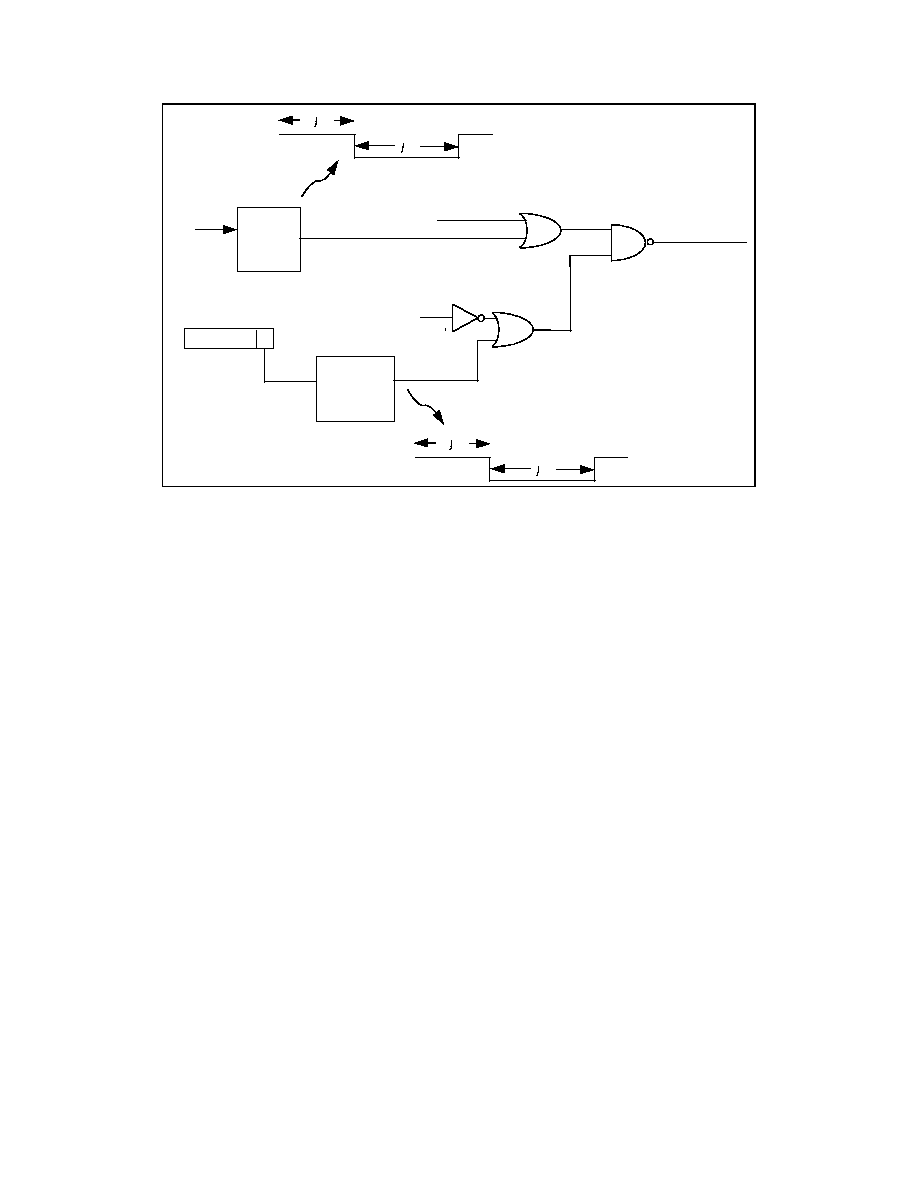
187
CPU_RESET Logic Diagram
KRESET
Pulse
Gen
Port92 Reg
Pulse
Gen
CPU_RESET
ENAB_P92
FE
Command
Bit 0
From
KRESET
Speed up
Logic
6us
14 us
6us
14 us
nALT_RST
SAEN
FIGURE 9 - CPU_RESET IMPLEMENTATION DIAGRAM

188
Port 92
The FDC37C957FR supports ISA I/O writes to port 92h as a quick alternate mechanism for
generating a CPU_RESET pulse or controlling the state of GATEA20.
Port 92 Register Description
D7-D2
D1
D0
Host R/W
R/W
R/W
R/W
Bit Def
0
Reserved
ALT_GATEA20
ALT_CPU_RESET
The Port92h register resides at ISA address 0x92 and is used to support the alternate reset
(nALT_RST) and alternate GATEA20 (ALT_A20) functions. This register defaults to 0x00 on
assertion of RESET_OUT or on VCC2 Power On Reset.
The Port92h Register is enabled by setting the Port 92 Enable bit (bit-0 of Logical Device 7
Configuration Register 0xF0). When Port92 is disabled, by clearing the Port 92 Enable bit, then
access to this register is completely disabled ( I/O writes to ISA 92h are ignored and I/O reads float
the system data bus SD[7:0]).
When Port92h is enabled the bits have the following meaning:
D7-D2 : [Reserved]
Writes are ignored and reads return 0.
D1 : [ALT_GATEA20]
This bit provides an alternate means for system control of the Orion's GATEA20 pin.
= 0 : ALT_A20 is driven low.
= 1 : ALT_A20 is driven high.
When Port 92 is enabled, writing a 0 to bit-1 of the Port92 Register forces ALT_A20 low. ALT_A20
low drivesGATEA20 low, if A20 from the keyboard controller is also low. When Port 92 is enabled,
writing a 1 to bit-1 of the Port92 register forces ALT_A20 high. ALT_A20 high drives GATEA20 high
regardless of the state of A20 from the keyboard controller.
D0: [ALT_CPU_RESET]
This bit provides an alternate means to generate a CPU_RESET pulse. The CPU_RESET output
provides a means to reset the system CPU to effect a mode switch from Protected Virtual Address
Mode to the Real Address Mode. This provides a faster means of reset than is provided through the
8051 Keyboard controller. Writing a `1' to this bit will cause the nALT_RST internal signal to pulse
(active low) for a minimum of 6
µ
s after a delay of 14
µ
s. Before another nALT_RST pulse can be
generated, this bit must be written back to zero.

189
Direct Keyboard Scan
The FDC37C957FR Scanning Keyboard Controller is designed for intelligent keyboard management
in computer applications. By properly configuring GPIO4 and GPIO5 the FDC37C957FR may be
programmed to directly control keyboard interface matrixes of up to 16x8.
Keyboard Scan-out register
Host
N/A
8051
0x7F04 (W)
Power
VCC1
Default
0x20
D7-D6
D5
D4
D3
D2
D1
D0
8051 R/W
W
W
W
W
W
W
W
Bit Def
N/A
KSEN
1 = forces
all KSO
lines to go
low
D5 and D4 must be `0'
D[3:0] = 0000 KSO[0] is asserted low
D[3:0] = 0001 KSO[1] is asserted low
D[3:0] = 0010 KSO[2] is asserted low
D[3:0] = 0011 KSO[3] is asserted low
∑
∑
∑
D[3:0] = 1101 KSO[13] is asserted low
D[3:0] = 1110 KSO[14] is asserted low
D[3:0] = 1111 KSO[15] is asserted low
KSEN
1 = disable scanning of internal keyboard (all the KSOUT lines going high)(D4-D0 are don't
cares)
0 = enable scanning of internal keyboard
Note : To support KSO14 and KSO15, GPIO4 and GPIO5 must be configured properly.

190
Keyboard Scan-in register
Host
N/A
8051
0x7F04 (R)
Power
VCC1
Default
N/A
D7-D0
8051 R
R
Bit description
Reflects the state of KSI [7:0]
The value of the KSI[x] pins can be read through this register.
The pin values are latched during the read.
EXTERNAL KEYBOARD AND MOUSE INTERFACE
Industry-standard PC-AT-compatible keyboards employ a two-wire, bidirectional TTL interface for
data transmission. Several sources also supply PS/2 mouse products that employ the same type of
interface. To facilitate system expansion, the FDC37C957FR provides four pairs of signal pins that
may be used to implement this interface directly for an external keyboard and mouse.
The FDC37C957FR has four high-drive, open-drain output
(1)
,bidirectional port pins that can be used
for external serial interfaces, such as ISA external key-board and PS/2-type mouse interfaces. They
are KBCLK, KBDAT, EMCLK, EMDAT, IMCLK, IMDAT, PS2CLK and PS2DAT.
NOTE:
1. External pull-ups are required.
(The following function is assumed to be in the PS/2 PORT logic) The serial clock lines, KBCLK,
EMCLK, IMCLK and PS2CLK, are cleared to a low by VCC2 POR. This is so that any power-on
self-test completion code transmitted from the serial keyboard will not be missed by the
FDC37C957FR due to power-up timing mis-matches.

191
MailBox Register Interface
The FDC37C957FR provides a set of 16 8-bit registers, called mailbox registers, by which the Host
CPU may communicate with the 8051. These registers are accessible to the Host in Configuration
Mode or through the Open Mode Index and Data Registers also described in Configuration Section of
this specification. At the same time these registers are accessible to the 8051 through 16 memory
mapped control registers. 14 of these mailbox registers are general purpose and are typically used
to pass status and parameters. The remaining two mailbox registers (mbox-0 : System-to-8051, and
mbox-1 : 8051-to-System) are specifically designed to pass commands and to provide a means for
each to interrupt the other assuming interrupts are unmasked. These registers are not "Dual-ported"
meaning that the System BIOS and Keyboard BIOS must be designed to properly share these
registers.
Note: when the Host CPU performs a write of the System-to-8051 mailbox register an 8051 INT1 will
be generated and seen by the 8051 if unmasked. When the 8051 writes to the System-to-8051
mailbox register the data is blocked but the write forces the System-to-8051 register to clear to zero,
providing a means for the 8051 to inform that Host that an operation has been completed.
Note: when the 8051 performs a write of the 8051-to-System mailbox register an SMI may be
generated and seen by the Host if unmasked. When the Host CPU writes to the 8051-to-System
mailbox register the data is blocked but the write forces the 8051-to-System register to clear to zero,
providing a means for the Host to inform that 8051 that an operation has been completed.
The protocol used to pass commands back and forth through the mailbox interface is left to the
system designer. SMC can provide an application example of working code in which the Host uses
the Mailboxes to gain access to all of the 8051 access only registers.

192
MAILBOX - Block Diagram
14, 8-bit
Mail-Box
Registers
HOST CPU
8051
8051-to-System
System-to-8051
SMI
INT1
Register Description
System-to-8051 Mailbox register 0
Host
IDX 0x82
8051
0x7F08 (RC)
Power
VCC1
Default
0x00
RC = Read only register is cleared upon a read.
If enabled, an INT1 will be generated when the System writes to this register. The Interrupt source
bit will be cleared when the 8051 reads this register. After reading this register the 8051 (8051) can
clear the register's content by a dummy write to this register to signify the System the register has
been read.
8051-to-system Mailbox register 1
Host
IDX 0x83
(RC)
8051
0x7F09
Power
VCC1
Default
0x00
If enabled by ESMI register, an SMI will be generated when the 8051 writes to this register. The SMI
interrupt will be cleared when the Host reads this register. After reading this register the system can

193
clear the register's content by a dummy write to this register to signify the 8051 the register has been
read.
Mailbox register 2-F
Host
IDX 0x84 -
0x91
8051
0x7F0A -
0x7F17
Power
VCC1
Default
0x00
These registers are readable and write-able from both the 8051 and the system. The system and the
8051 codes must make sure these registers are not inadvertently overwritten.
MBOX SMI Interrupt
The Host can enable/disable SMI interrupts generated as a result of the 8051 writing to Mailbox
Register 1. The Host can read the ESMI source register to determine if the FDC37C957FR Mailbox
interface was the cause of the SMI.
ESMI mask register
Host
IDX 0x97 (R)
8051
N/A
Power
VCC2
Default
0x00
D7-D4
D3
D2-D0
8051 R/W
N/A
N/A
N/A
System R/W
R
R/W
R
Bit Def
Reserved
1 = mask the 8051-to-system mailbox SMI
Reserved
ESMI source register
Host
IDX 0x96
8051
N/A
Power
VCC2
Default
0x00

194
D7-D4
D3
D2-D0
8051 R/W
N/A
N/A
N/A
System
R/W
R
R/W
R
Bit Def
Reserved
1 = 8051-to-system mailbox has been written to.
This bit is cleared by a read of Mailbox Register 1
Reserved
PS/2 Interface Description
PS/2 Port Control registers
Port 1
Port 2
Host
N/A
N/A
8051
0x7F41
0x7F49
Power
VCC2
VCC2
Default
0x00
0x00
D7
D6
D5
D4
D3
D2
D1
D0
R/W
R
R
R
R/W
R/W
R/W
R/W
R/W
PS/2
port1
Reserved
Reserved
Reserved
EM_EN
KB_EN
Inhibit
RX_EN
TX_EN
PS/2
port2
Reserved
Reserved
Reserved
IM_EN
PS2_EN
Inhibit
RX_EN
TX_EN
Only one of bits 2-0 can be set to one.
PS/2 Port Status registers
Port 1
Port 2
Host
N/A
N/A
8051
0x7F42 (R)
0x7F4A (R)
Power
VCC2
VCC2
Default
0x00
0x00
D7
D6
D5
D4
D3
D2
D1
D0
R/W
R
R
R
R
R
R
R
R
PS/2
port1
Reserved
Reserved
EM_busy
KB_busy
Inhibit
done
EM_drdy
KB_drdy
Error
PS/2
port2
Reserved
Reserved
IM_busy
PS2_busy
Inhibit
done
IM_drdy
PS2_drdy
Error

195
PS/2 Port Error Status registers
Port 1
Port 2
Host
N/A
N/A
8051
0x7F43 (R)
0x7F4B (R)
Power
VCC2
VCC2
Default
0x00
0x00
D7-D5
D4
D3
D2
D1
D0
R/W
R
R
R
R
R
R
Bit Def
Reserved
Parity
RES_timeout
REC_timeout
RTS_timeout
XMT_timeout
PS/2 Port Tansmit rgsiters
Port 1
Port 2
Host
N/A
N/A
8051
0x7F44 (W)
0x7F4C (W)
Power
VCC2
VCC2
Default
0x00
0x00
D7
D6
D5
D4
D3
D2
D1
D0
R/W
W
W
W
W
W
W
W
W
PS/2 port receive registers
Port 1
Port 2
Host
N/A
N/A
8051
0x7F45 (R)
0x7F4D (R)
Power
VCC2
VCC2
Default
0x00
0x00
D7
D6
D5
D4
D3
D2
D1
D0
R
R
R
R
R
R
R
R
R
Access Bus Interface Description
The Access.Bus interface is fully and directly controlled by the on-chip 8051 through its set of on-chip
memory mapped control registers. The Access.Bus logic is based on the PCF8584 I2C controller
and is powered on the VCC1 powerplane to provide the ability to wake-up the 8051 on an
Access.Bus event.

196
Memory Mapped Control Registers
ACCESS.BUS Control register
Host
N/A
8051
0x7F31 (W)
Power
VCC1
Default
0x00
D7
D6
D5
D4
D3
D2
D1
D0
8051 R/W
W
W
W
W
W
W
W
W
Bit Def
PIN
ES0
Reserved
Reserved
ENI
STA
STO
ACK
Bit-7 PIN : (Pending Interrupt Not). Writing this bit to a logic `1' deasserts all status bits except for
BB# (Bus Busy) - BB# is not affected. This is a self-clearing bit. Writing this bit to a logic
`0' has no effect.
ACCESS.BUS Status register
Host
N/A
8051
0x7F31 (R)
Power
VCC1
Default
0x81
D7
D6
D5
D4
D3
D2
D1
D0
8051 R/W
R
R
R
R
R
R
R
R
Bit Def
PIN
0
STS
BER
LRB
AAS
LAB
BB#
ACCESS.BUS Own Address register
Host
N/A
8051
0x7F32
Power
VCC1
Default
0x00
D7
D6
D5
D4
D3
D2
D1
D0
8051
R/W
R/W
R/W
R/W
R/W
R/W
R/W
R/W
R/W
Bit
Def
Reserved
Slave
Address
6
Slave
Address
5
Slave
Address
4
Slave
Address
3
Slave
Address
2
Slave
Address
1
Slave
Address
0

197
ACCESS.BUS Data register
Host
N/A
8051
0x7F33
Power
VCC1
Default
0x00
D7
D6
D5
D4
D3
D2
D1
D0
8051 R/W
R/W
R/W
R/W
R/W
R/W
R/W
R/W
R/W
ACCESS.BUS Clock register
Host
N/A
8051
0x7F34
Power
VCC1
Default
0x00
ACCESS.BUS Clock
D7
D6-D2
D1
D0
8051 R/W
R/W
R
R/W
R/W
AB_RST
*
Reserved
00 - clock off (default)
01 - 32Khz Clock
10 - 8051 clock
11 - 24Mhz clock
(*) Access Bus Reset, not self-clearing, must be written high and then written low.
Bit-7 AB_RST: (Access.bus Reset) setting this bit re-initializes all logic and registers in the
Access.bus block.

198
Table 63 - Access.Bus Clock Rates
Access
Bus Clock
Clock Rate
Data Rate
Nominal
High
Nominal
Low
Minimum
High
D[1:0]
00
Off
10
Ring Osc
f/240
96/f
144/f
18/f
Ring Osc=4Mhz
16.7Khz
24
µ
s
36
µ
s
4.5
µ
s
Ring Osc=6Mhz
25Khz
16
µ
s
24
µ
s
3
µ
s
Ring Osc=8Mhz
33.3Khz
12
µ
s
18
µ
s
2.25
µ
s
10
12Mhz
50Khz
8
µ
s
12
µ
s
4
µ
s
10
14.3... Mhz
60Khz
6.7
µ
s
10.1
µ
s
4
µ
s
10
16Mhz
67Khz
6
µ
s
9
µ
s
4
µ
s
11
24 Mhz
100Khz
4
µ
s
6
µ
s
4
µ
s
f = frequency of the ring oscillator.
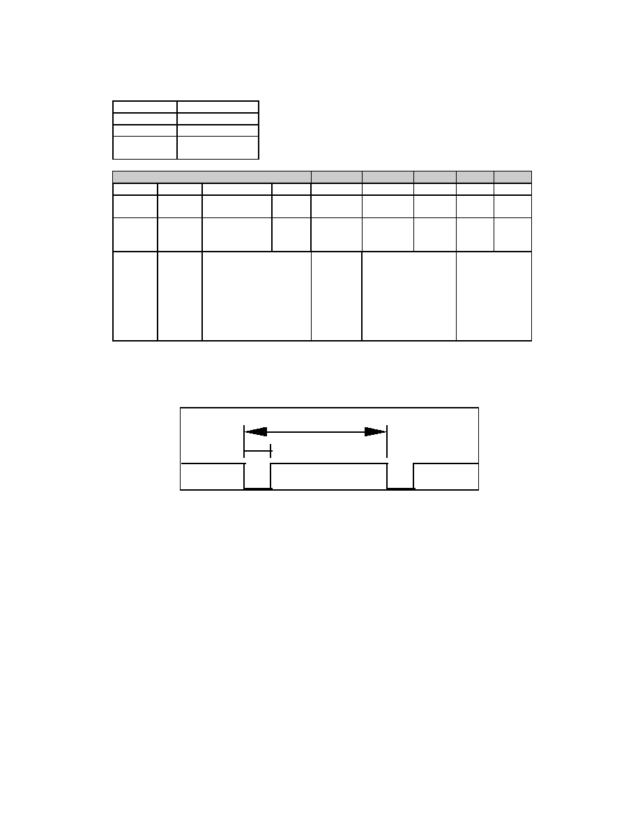
199
LED Controls
The FDC37C957FR has three independent LED outputs that are programmable under 8051 control.
LED register
Host
N/A
8051
0x7F21
Power
VCC1
Default
0x00 on VCC2
POR
D7
D6
D5
D4
D3
D2
D1
D0
Default
0
0
0
N/A
0
0
0
0
8051
access
R/W
R/W
R/W
R
R/W
R/W
R/W
R/W
Bit def
FDD
Led
Enable
FDD_LED1
FDD_
LED0
status of
pin
MODE
PWR_LE
D1
PWR_
LED0
BAT_
LED1
BAT_
LED0
Note 1
00 FDD LED is off
01 LED flash; P=1.0
sec
10 LED flash; P=0.5
sec
11 LED is fully on
00 PWR LED is off
01 LED flash;
P=3.0 sec
10 LED flash;
P=1.5 sec
11 LED is fully on
00 Battery
LED is off
01 LED flash;
P=1.0 sec
10 LED flash;
P=0.5 sec
11 LED is
fully on
Note 1: D7 =1; FDD_LED Pin is controlled by D6,D5
D7=0; FDD_LED is controlled by the Motor Enable 0 pin from the FDC. When Motor Enable
0 pin is asserted the LED is on.
LED on time is T=125msec; "0" is on, "1" is off. Period "P" is indicated above.
P
T
FIGURE 10 - LED OUTPUT
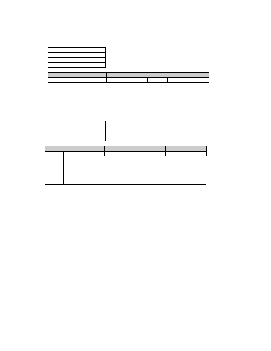
200
Pulse Width Modulators
The FDC37C957FR has two independent Pulse Width Modulator outputs that are programmable
under 8051 control.
PWM0 register
Host
IDX 0x92
8051
0x7F25
Power
VCC1
Default
0x00
D7
D6
D5
D4
D3
D2
D1
D0
0 =
select
2 Mhz
1 =
select
3 MHz
These 7 bits control the duty cycle of pin PWM0 (FAN_SPD)
0000000 =pin is low
0111111 = 50% duty cycle (32us on/ 32 us off if 2 Mhz is used)
1111111 = pin is high for 127, low for 1
PWM1 register
Host
IDX 0x93
8051
0x7F26
Power
VCC1
Default
0x00
D7
D6
D5
D4
D3
D2
D1
D0
0 =
select
2 Mhz
1 =
select
3 MHz
These 7 bits control the duty cycle of pin PWM1
0000000 =pin is low
0111111 = 50% duty cycle (32us on/ 32 us off if 2 Mhz is used)
1111111 =pin is high for 127, low for 1

201
Real Time Clock CMOS Access
RTCCNTRL (RTC Control) Register
Host
N/A
8051
0x7FF5
Power
VCC1
Default
0x80
This chip implements an interface that allows the 8051 to read/write the RTC and CMOS registers.
When RESET_OUT is active or when VCC2 is off, the 8051 can read and write the CMOS.
D7
D6
D5
D4
D3
D2
D1
D0
nSH
0
0
0
KREQH
HREQH
KREQL
HREQL
nSH
nSmart Host - This bit is controlled by the 8051. When set to a '1', the host is not a smart
host and does not recognize the sharing protocol. When set to a '0', the host is smart and
can recognize the sharing protocol. When Set to One, this bit will clear HREQH and
HREQL; then clearing this bit to zero will allow the 8051 to regain access to the CMOS
RAM.
KREQL
Keyboard Request Low- This bit can be set by the 8051 when HREQL IS '0'. If the
request is not granted, this bit is read back as a zero and the request must be tried again.
Note: After regaining control of the CMOS, the 8051 must re-write the RTC Address
register before accessing the RTC Data Register. This bit selects access to the CMOS
RAM Addresses 0-7F.
HREQL
Host Request Low- This bit can be set by the host when KREQL IS '0'. If the request is
not granted, this bit is read back as a zero and the request must be tried again.
KREQH
Keyboard Request High- This bit can be set by the 8051 when HREQH IS '0'. If the
request is not granted, this bit is read back as a zero and the request must be tried again.
Note: After regaining control of the CMOS, the 8051 must re-write the RTC Address
register before accessing the RTC Data Register. This bit selects access to the CMOS
RAM Addresses 80-FF.
HREQH Host Request High- This bit can be set by the host when KREQH IS '0'. If the request is
not granted, this bit is read back as a zero and the request must be tried again.
nSH
KREQx
HREQx
Bus Access
1
x
x
Host
0
0
0
None
0
1
0
8051
0
0
1
Host

202
RTC Address Register (High and Low)
Host
N/A
8051
0x7FF8 &
0x7FF6
Power
VCC1
Default
0x00 & 0x00
The low register is used to provide the address for the first bank of 128 CMOS RAM registers and
the high register is used to provide the address for the 2nd bank of 128 CMOS RAM registers for a
total of 255 registers. This register is used to select the CMOS address when KREQ=1. CMOS
register 7F is a control registers that reflects the RTC Control register and can not be used as general
purpose storage. Bit D7 is not used for the address decode and is a don't care bit.
RTC Data Register (High and Low)
Host
N/A
8051
0x7FF9 &
0x7FF7
Power
VCC1
Default
0x00 & 0x00
The low register is used to access CMOS RAM the first bank of 128 bytes the high register is used to
access the 2nd bank of 128 registers . This register is used to read or write the selected CMOS
register when KREQ=1.

203
8051 Controlled Parallel Port
To facilitate activities such as reprogramming the Flash Memory without opening the unit, the 8051 is
able to take control of the parallel port interface. The 8051 has three memory mapped registers that
look like the host's standard parallel port registers (Status, Control, and Data) with the exception that
the 8051's Parallel Port Status register contains a write bit (bit-0) that allows the 8051 to disconnect
the interface from the Host and take control. Refer to the Parallel Port section of this specification for
more information.
Block Diagram
FIGURE 11 - PARALLEL PORT MULTIPLEXOR
SEL 1
From/to Host Parallel port interface
Parallel Port
Parallel Port connector
From/to 8051 Parallel port interface
PP_HA
1
0
Parallel Port multiplexer

204
Operation Registers
The 8051 uses the following three memory mapped register to gain access to and control the parallel
port interface.
PAR PORT STATUS Register
Host
N/A
8051
0x7F3A
Power
VCC2
Default
0x00
D7
D6
D5
D4
D3
D2
D1
D0
8051
R/W
R
R
R
R
R
R
R
R/W
System
R/W
N/A
N/A
N/A
N/A
N/A
N/A
N/A
N/A
Bit Def
nBUSY
nACK
PE
SLCT
nERR
0
0
PP_HA
1 = Host (or FDC)
controls the
Parallel Port
Interface.
0 = 8051 controls
the Parallel Port
Interface(default).
If 8051 access to the parallel port pins is enabled: The level of the parallel port status pins can be
read by reading this register.
Bit D7 (nBUSY) : reflects the inverse state of pin BUSY
Bit D6 (nACK)
: reflects the current state of pin nACK
Bit D5 (PE)
: reflects the current state of pin PE
Bit D4 (SLCT)
: represents the current state of pin SLCT
Bit D3 (nERR)
: reflects the current state of pin nERR
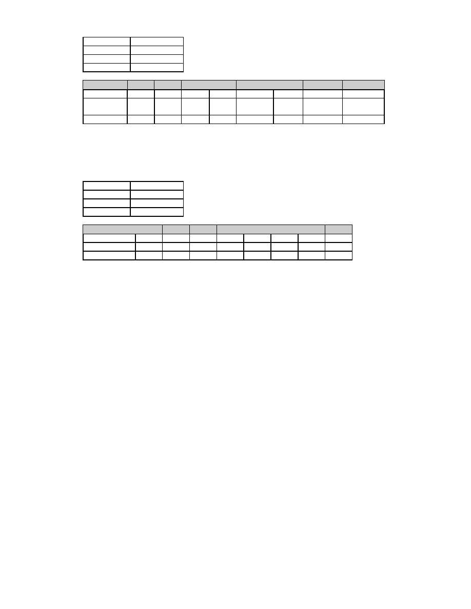
205
PAR PORT CONTROL Register
Host
N/A
8051
0x7F3B
Power
VCC2
Default
0x00
D7
D6
D5
D4
D3
D2
D1
D0
8051 R/W
R/W
R/W
R/W
R/W
R/W
R/W
R/W
R/W
System
R/W
N/A
N/A
N/A
N/A
N/A
N/A
N/A
N/A
Bit Def
0
0
PCD
0
SLCTIN
nINIT
AUTOFD
STROBE
If 8051 access to the parallel port pins is enabled:
The value of STROBE, AUTOFD and SLCTIN are inverted and output onto the parallel port control
pins. The value of nINIT is output onto the parallel port control pins. If PCD (Parallel Control
Direction) = 0, the data bus is output. If PCD = 1 the parallel port data bus is floating to allow read
data in.
PAR PORT DATA Register
Host
N/A
8051
0x7F3C
Power
VCC2
Default
0x00
D7
D6
D5
D4
D3
D2
D1
D0
8051 R/W
R/W
R/W
R/W
R/W
R/W
R/W
R/W
R/W
System R/W
N/A
N/A
N/A
N/A
N/A
N/A
N/A
N/A
Bit Def
PD7
PD6
PD5
PD4
PD3
PD2
PD1
PD0
If 8051 access to the parallel port pins is enabled: When read, this register reads the logic levels on
the parallel port pins.
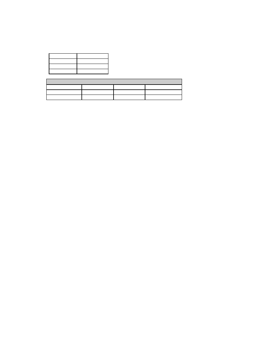
206
8051 Controlled IR Port
It is possible to give direct control of the IRRX and IRTX pins to the 8051 by setting bit-2 of the
Multiplexing_1 Register. The 8051 communicates to the Pins through its Memory Mapped IR Data
Register shown here.
IR Data register
Host
IDX 0x98
8051
N/A
Power
VCC2
Default
0x00
D7-D2
D1
D0
8051 R/W
N/A
N/A
N/A
System R/W
R/W
R
R/W
Bit Def
Reserved
IR_REC
IR_TX
Bit 1 and bit 0 are don't care if bit 2 of the Multiplexing_1 Register is reset. (These bits are
multiplexed onto the IRTX and IRRX pins when bit-2 of the Multiplexing register is set).

207
General Purpose I/O (GPIO)
Functional Block Diagrams
GPIO OUT REG BIT
OUTPUT EN
ALT FUNC
Control bit
ALT FUNC OUTPUT
OUT PIN
1
0
nRD
nWR
FIGURE 12 - OUTPUT PIN TYPE
IN REG BIT
IN PIN
Wake-up Source Bit
nRD
Edge detector
Wake-up Mask Bit
nWR
Wake-up
IRQ
FIGURE 13 - INPUT PIN TYPE
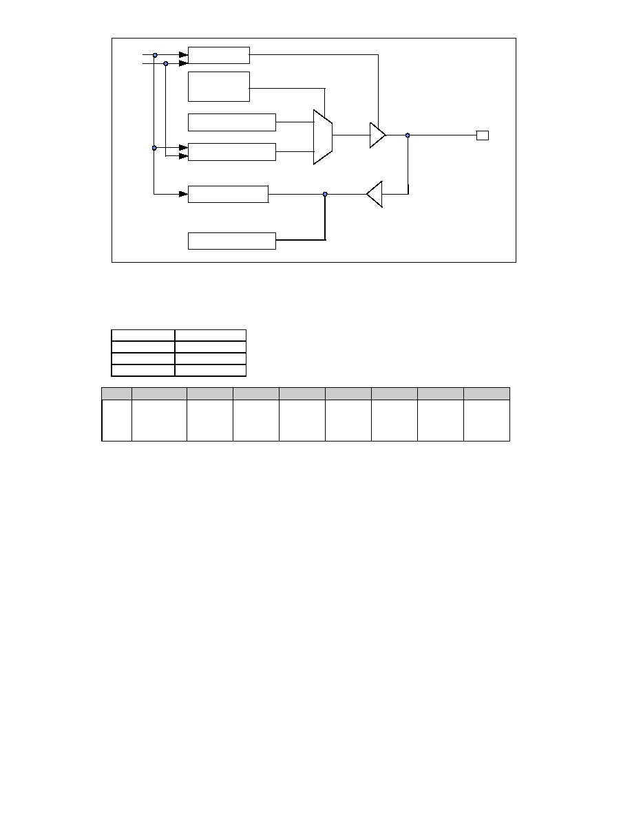
208
GPIO OUT REG BIT
GPIO IN REG BIT
GPIO DIR BIT
ALT FUNC
Control bit
ALT FUNC OUTPUT
GPIO PIN
1
0
ALT FUNC INPUT
nRD
nWR
FIGURE 14 - GPIO PIN TYPE
Memory Mapped Control Registers
GPIO Direction register A
Host
N/A
8051
0x7F18
Power
VCC1
Default
0x00
D7
D6
D5
D4
D3
D2
D1
D0
Bit
Def
GPIO7
1=output
0=input
GPIO6
1=out-
put
0=input
GPIO5
1=out-
put
0=input
GPIO4
1=out-
put
0=input
GPIO3
1=out-
put
0=input
GPIO2
1=out-
put
0=input
GPIO1
1=out-
put
0=input
GPIO0
1=out-
put
0=input

209
GPIO Input register A
Host
N/A
8051
0x7F1A (R)
Power
VCC1
Default
N/A
D7
D6
D5
D4
D3
D2
D1
D0
Bit
description
status
of pin
GPIO7
status
of pin
GPIO6
status
of pin
GPIO5
status
of pin
GPIO4
status
of pin
GPIO3
status
of pin
GPIO2
status
of pin
GPIO1
status
of pin
GPIO0
GPIO Output register A
Host
N/A
8051
0x7F19
Power
VCC1
Default
0x00
D7
D6
D5
D4
D3
D2
D1
D0
Bit
description
GPIO7
GPIO6
GPIO5
GPIO4
GPIO3
GPIO2
GPIO1
GPIO0
GPIO Direction register B
Host
N/A
8051
0x7F1B
Power
VCC1
Default
0x00
D7
D6
D5
D4
D3
D2
D1
D0
Bit Def
GPIO15
1=out-
put
0=input
GPIO14
1=out-
put
0=input
GPIO13
1=out-
put
0=input
GPIO12
1=out-
put
0=input
GPIO11
1=out-
put
0=input
GPIO10
1=out-
put
0=input
GPIO9
1=out-
put
0=input
GPIO8
1=out-
put
0=input

210
GPIO Output register B
Host
N/A
8051
0x7F1C
Power
VCC1
Default
0x00
D7
D6
D5
D4
D3
D2
D1
D0
Bit Def
GPIO
15
GPIO
14
GPIO
13
GPIO
12
GPIO
11
GPIO
10
GPIO
9
GPIO
8
GPIO Input register B
Host
N/A
8051
0x7F1D (R)
Power
VCC1
Default
N/A
D7
D6
D5
D4
D3
D2
D1
D0
Bit Def
status
of pin
GPIO15
status
of pin
GPIO14
status
of pin
GPIO13
status
of pin
GPIO12
status
of pin
GPIO11
status
of pin
GPIO10
status
of pin
GPIO9
status
of pin
GPIO8
GPIO Direction register C
Host
N/A
8051
0x7F1E
Power
VCC1
Default
0x00 on VCC2
POR
D7
D6
D5
D4
D3
D2
D1
D0
Bit
Des.
0
0
GPIO21
1=output
0=input
GPIO20
1=output
0=input
GPIO19
1=output
0=input
GPIO18
1=output
0=input
GPIO17
1=output
0=input
GPIO16
1=output
0=input

211
GPIO Output register C
Host
N/A
8051
0x7F1F
Power
VCC1
Default
0x00 on VCC2
POR
D7
D6
D5
D4
D3
D2
D1
D0
Bit Def.
0
0
GPIO21
GPIO20
GPIO19
GPIO18
GPIO17
GPIO16
GPIO Input register C
Host
N/A
8051
0x7F20 (R)
Power
VCC1
Default
N/A
D7
D6
D5
D4
D3
D2
D1
D0
Bit
def
0
0
status of
pin
GPIO21
status of
pin
GPIO20
status of
pin
GPIO19
status of
pin
GPIO18
status of
pin
GPIO17
status of
pin
GPIO16
OUT register D
Host
N/A
8051
0x7F22
Power
VCC1
Default
0xFF on VCC2
POR
D7
D6
D5
D4
D3
D2
D1
D0
Bit Def
OUT7
OUT6
OUT5
OUT4
OUT3
OUT2
OUT1
OUT0

212
OUT register E
Host
N/A
8051
0x7F23
Power
VCC1
Default
0x0F on VCC2
POR
D7
D6
D5
D4
D3
D2
D1
D0
Bit Def
0
0
0
0
OUT11
OUT10
OUT9
OUT8
IN register F
Host
N/A
8051
0x7F24 (R)
Power
VCC1
Default
N/A
D7
D6
D5
D4
D3
D2
D1
D0
Bit Def
status
of pin
IN7
status
of pin
IN6
status
of pin
IN5
status
of pin
IN4
status
of pin
IN3
status
of pin
IN2
status
of pin
IN1
status
of pin
IN0
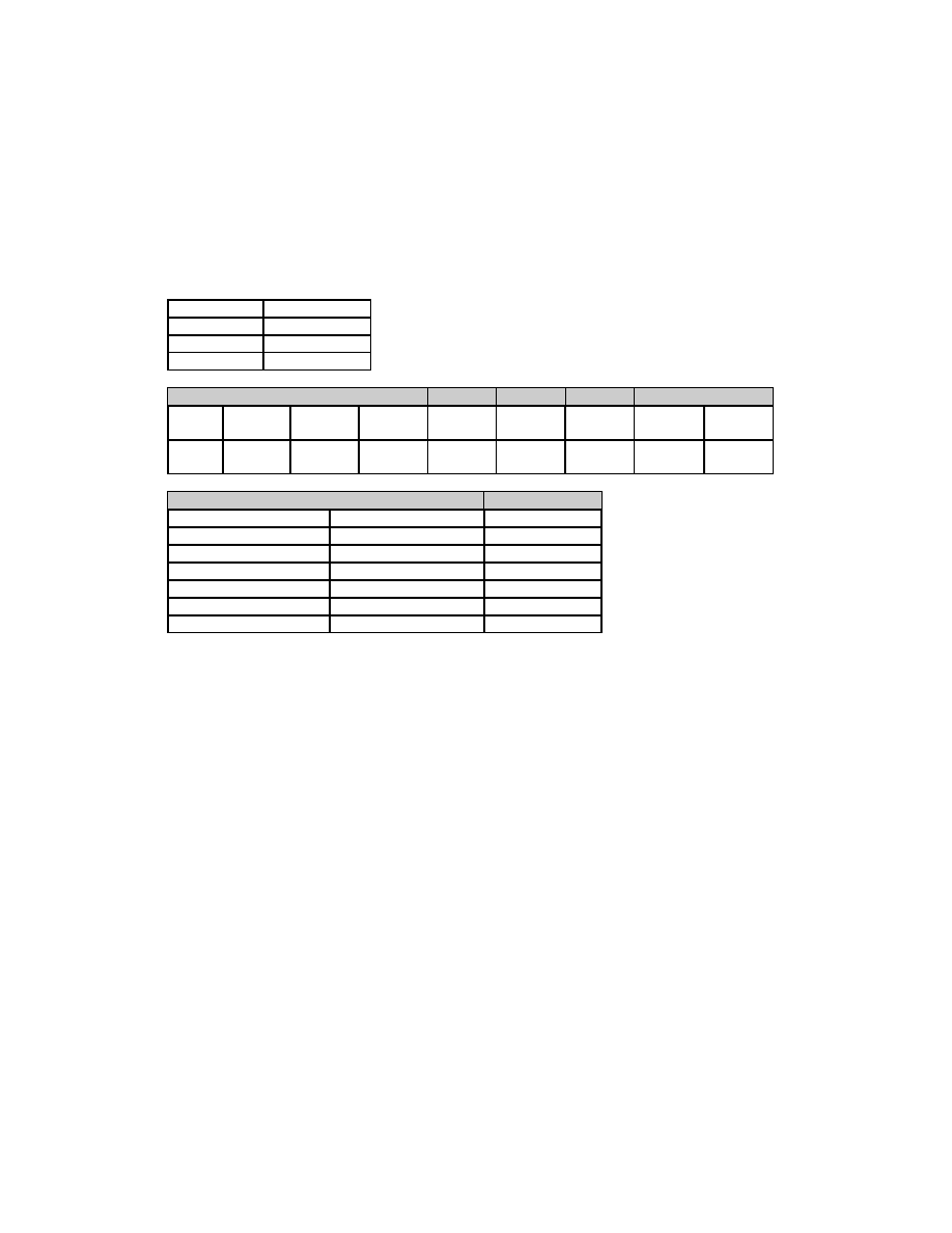
213
Multiplexed Pins
Many of the FDC37C957FR's GPIO pins provide specific alternate functions which may be enabled
by the 8051 firmware based on the design of the system that the part will be used in.
List
Refer to the Alternate Function Pin List Section in this specification for a complete list of all of the
FDC37C957FR multifunction pins.
Control Registers
The 8051 firmware controls the multiplexing functions for each of the Multiplexed pins on the
FDC37C957FR through the registers described in this section.
Multiplexing_1 register:
Host
N/A
8051
0x7F3D
Power
VCC1
Default
0x00
D7
D6
D5
D4
D3
D2
D1
D0
8051
R/W
R/W
R/W
R/W
R/W
R/W
R/W
R/W
R/W
Bit
Def
MISC7
MISC6
MISC5
MISC4
MISC3
MISC2
MISC1
MISC0
Pin
MISC0 = 0 (default)
MISC0 = 1
IRQ6(FDC)/OUT0
OUT0
IRQ6(FDC)
nIRQ8/OUT1
OUT1
nIRQ8
IRQ7(PP)/OUT2
OUT2
IRQ7(PP)
IRQ12(Mouse)/OUT3
OUT3
IRQ12(Mouse)
IRQ1(KBD)/OUT4
OUT4
IRQ1(KBD)
nSMI/OUT7
OUT7
nSMI
SIRQ/IRQ3(UA1)
SIRQ
IRQ3(UA1)

214
MISC[3,1]
Pin
GPIO[20]
Pin 52
Pin
GPIO[21]
Pin 53
[0,0] (default)
GPIO[20] +
8051_RX *
GPIIO[21]
[0,1]
PS2CLK
PS2DAT
[1,0]
GPIO[20] +
8051_RX *
8051_TX **
[1,1]
PS2CLK
PS2DAT
* GPIO20_DIR bit should be set to 0 when operating as an 8051_RX pin.
** GPIO21_DIR bit must be set to 1 when operating as an 8051_TX pin.
The PS/2 pins on GPIO20 and GPIO21 are disabled (internally pulled high) when the non PS/2
alternate functions are selected. The PS/2 inputs under this condition are seen as a high to the PS/2
Device Interface logic.
Whenever a PS/2 channel is not enabled, the input signals to that channel must be high. The
FDC37C957FR provides this through the use of weak pull-ups since the EM and KB channels share a
common receive path and the IM and PS2 channels also share a common receive path.
1
0
PIN 52
GPIO20_DIR
MISC1
PS2_CLK_OUT
GPIO20_OUT
GPIO20_IN
PS2_CLK_IN
8051_RX
FIGURE 15 - GPIO[20] ALTERNATE FUNCTION STRUCTURE

215
1
0
PIN 53
MISC1
MISC3
8051_TX
GPIO21_OUT
GPIO21_IN
PS2_DAT_IN
0
1
PS2_DAT_OUT
GPIO21_DIR
FIGURE 16 - GPIO21 ALTERNATE FUNCTION STRUCTURE
Pin
MISC2 = 0 (default)
MISC2 = 1
IRTX
from IrCC Block
from IR Data Register
IRRX
from IrCC Block
from IR Data Register
Pin
MISC4 = 0 (default)
MISC4 = 1
PWM0/OUT10
OUT10
PWM0
PWM1/OUT11
OUT11
PWM1
Pin
MISC5 = 0 (default)
MISC5 = 1
OUT5
OUT5
nDS1
OUT6
OUT6
nMTR1
Pin
MISC6 = 0 (default)
MISC6 = 1
GPIO[ 17]
GPIO[17]
GateA20
Pin
MISC7 = 0 (default)
MISC7 = 1
GPIO[8]
GPIO[8]
IrCC Block COM-RX Port
GPIO[9]
GPIO[9]
IrCC Block COM-TX Port
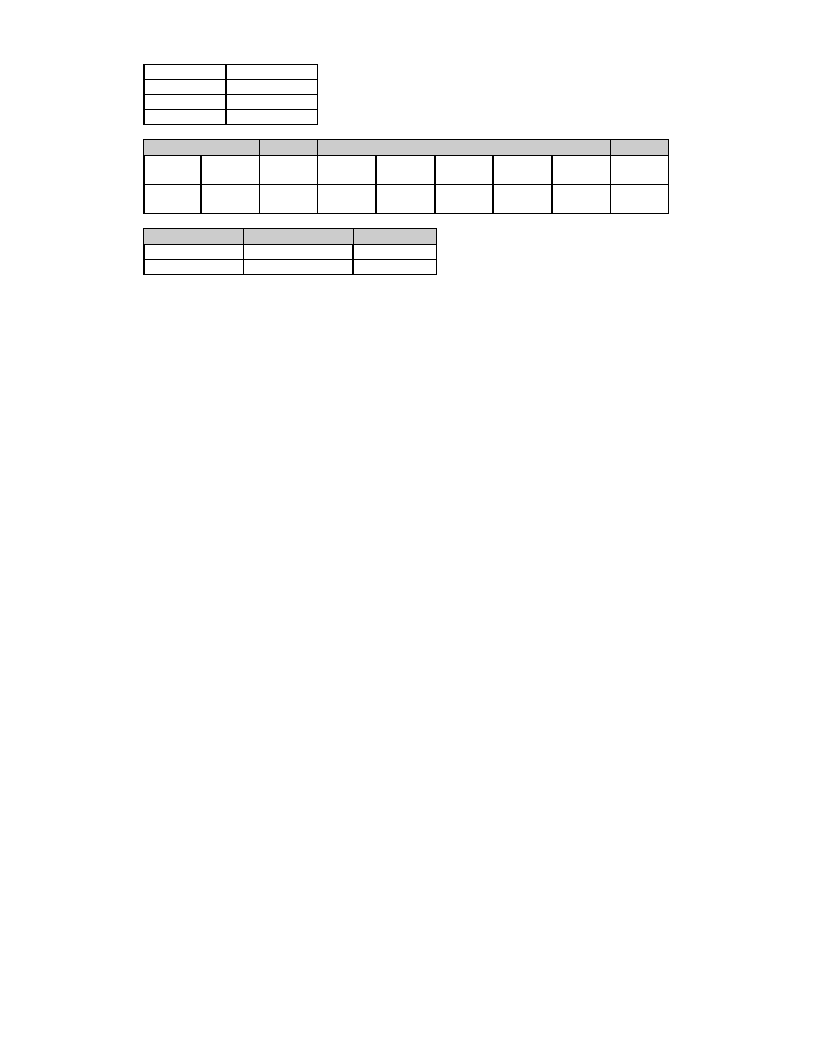
216
Multiplexing_2 register:
Host
N/A
8051
0x7F40
Power
VCC1
Default
0x00
D7
D6
D5
D4
D3
D2
D1
D0
8051
R/W
R/W
R/W
R/W
R/W
R/W
R/W
R/W
R/W
Bit Def
MISC
16
MISC
15
MISC
14
MISC
13
MISC
12
MISC
11
MISC
10
MISC
9
MISC9
Pin GPIO[4]
GPIO[5]
0 (default)
GPIO[4]
GPIO[5]
1
KSO14
KSO15
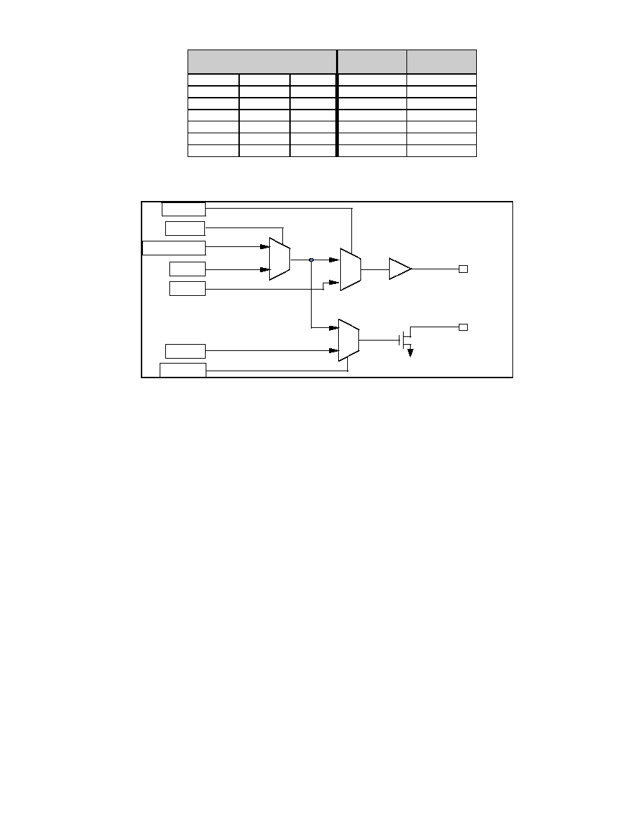
217
MISC17
MISC10
MISC6
Pin OUT[8]
(Pin 202)
Pin KSO12
(Pin 23)
0
0
0
OUT8
KSO12
0
0
1
CPU_RESET
KSO12
0
1
X
DRQ2
KSO12
1
0
0
OUT8
OUT8
1
0
1
CPU_RESET
CPU_RESET
1
1
0
DRQ2
OUT8
1
1
1
DRQ2
CPU_RESET
With this definition, only the pair [OUT8 & CPU_RESET] can not simultaneously exist on
pins 202 and 23.
1
0
P I N 2 0 2
M I S C 1 0
M I S C 6
C P U _ R E S E T
D R Q 2
M I S C 1 7
K S O 1 2
0
1
O U T 8
1
0
P I N 2 3
FIGURE 17 - PINS 202 AND 23 ALTERNATE FUNCTION OPERATION

218
MISC17
Pin GPIO18
(Pin 207)
Pin KSO13
(Pin 22)
0
GPIO18 +
nDACK2 (1)
KSO13
1
nDACK2
GPIO18
note 1: nDACK2 can be received on pin 207 when
MISC17=0 by setting GPIO18's DIR bit to 0.
P I N 2 0 7
M I S C 1 7
G P I O 1 8 _ D I R
K S O 1 3
G P I O 1 8 _ O U T
1
0
P I N 2 2
n D A C K 2
0
1
G P I O 1 8 _ I N
[ ( M I S C 1 7 = 0 ) | ( G P I O 1 8 _ D I R & M I S C 1 7 = 1 ) ]
FIGURE 18 - PIN 207 AND 22 ALTERNATE FUNCTION OPERATION
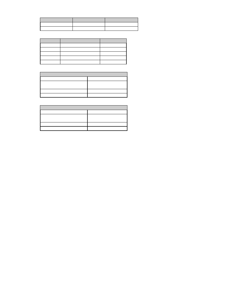
219
MISC11
Pin OUT[9]
Pin GPIO[19]
0 (default)
OUT[9]
GPIO[19]
1
DRQ3
nDACK3
Pin
MISC12 = 0 (default)
MISC12 = 1
GPIO[11]
GPIO[11]
nCTS2
GPIO[12]
GPIO[12]
nDTR2
GPIO[13]
GPIO[13]
nDSR2
GPIO[14]
GPIO[14]
nDCD2
GPIO[15]
GPIO[15]
nRI2
MISC[14:13] = 0 (default)
Pin GPIO[6]
[0:0] (default)
GPIO[6]
[0:1]
IR_MODE
(IrCC GP Data) output
[1:0]
FRX input
[1:1]
Reserved
MISC[16:15] = 0 (default)
Pin GPIO[10]
[0:0] (default)
GPIO[10]
[0:1]
IR_MODE
(IrCC GP Data) output
[1:0]
FRX input
[1:1]
nRTS2

220
Multiplexing_3 register:
Host
N/A
8051
0x7F30
Power
VCC1
Default
0x00
D7 - D2
D1
D0
8051 R/W
R
R/W
R/W
Bit Def
Reserved 0
MISC17
MISC8
Note : Originally Bit-7 in the Output Enable Register was defined as MISC8, but this bit is now
Reserved.
MISC8
Pin
GPIO[16]
0 (default)
GPIO[16]
1
MID1
MISC17 is described in the Multiplexing_2 register section.

221
REAL TIME CLOCK
GENERAL DESCRIPTION
The RTC SUPERCELL is a complete time of day clock with alarm and one hundred year calendar, a
programmable periodic interrupt, and a programmable square wave generator.
FEATURES
∑
Counts seconds, minutes, and hours of the day.
∑
Counts days of the week, date, month and year.
∑
Binary or BCD representation of time, calendar and alarm.
∑
24 hour daily alarm.
PORT DEFINITION AND DESCRIPTION
OSC
Clock Input Pin. Maximum clock frequency is 32.768 Khz.
DB[0:7]IN
CPU DATA BUS, All communication of data and control between the RTC
DB[0:7]OUT
and the CPU are carried out over this data bus.
A[0:7]
The 8 address lines which select which internal register is to be accessed by any
CPU operation.
nCS
Low active block select. This input is low during any CPU cycle in which the RTC is
to be accessed. (Active for addresses 70H, 71H and 74H, 76H)
nIOR
CPU output data strobe. This port is a low whenever the CPU reads data from an
internal RTC register. The nIOR low condition causes the contents of the addressed
register to output its data onto the Data Bus.
nIOW
CPU write data strobe. The low to high transition of this port latches the contents of
the data bus into the selected RTC register.

222
ISA I/O Interface
Table 64 - RTC ISA I/O Address Map
ISA Address
Function (Note 1)
Base (R/W)
Address Register (70H/74H)
Base+1 (R/W)
Data Register (71H/76H)
All addresses are qualified by AEN.
Note 1: The RTC can be enabled or disabled through the configuration registers.
RTC Address Register:
Writing to this register, sets the CMOS address that will be read or written. Port 70H (with RTC Data
register at 71H) is to address the first 128 CMOS bytes and port 74H (with RTC Data register at 76H)
is for the next 128 CMOS bytes. Bit D7 is not used for the CMOS RAM Address decoding. (All 8 bits
are read/write)
RTC Data Register:
A read of this register will read the contents of the selected CMOS register. A write to this register
will write to the selected CMOS register. (71H or 76H)

223
VCC1 POR
The VCC1 POR pin does not affect the clock calendar, or RAM functions. When VCC1 POR is
active the following occurs:
1. Periodic Interrupt Enable (PIE) is cleared to zero.
2. Alarm Interrupt Enable (AIE) bit is cleared to zero.
3. Update ended Interrupt Enable (UIE) bit is cleared to zero.
4. Update ended Interrupt Flag (UF) bit is cleared to zero.
5. Interrupt Request status Flag (IRQF) bit is cleared to zero.
6. Periodic Interrupt Flag (PIF) is cleared to zero.
7. The RTC and CMOS registers are not accessable.
8. Alarm Interrupt Flag (AF) is cleared to zero.
9. nIRQ pin is in high impedance state.
HOSTD
The HOST Disable pin, when active, prevents host access to the clock calendar, or
RAM functions. (Refer to Power Management)
8051D
The 8051 Disable pin, when active, prevents 8051 access to the clock calendar, or
RAM functions. (Refer to Power Management)
PS
The power-sense pin is used in the control of the Valid RAM and Time (VRT) bit in
Register D. When the PS pin is low, the VRT bit is cleared to zero. As power is
applied, the VRT bit remains low indicating that the contents of the RAM, Time
registers and Calendar are not guaranteed. PS must go high after powerup to allow
the VRT bit to be set by a read of Register D. This is an internal signal used to
detect if both the main power and the battery power were both low at the same
time. This is the only case where the contents of the RAM, Time registers and
Calendar are not valid.
nIRQ
The nIRQ pin is an active low output. The nIRQ output remains low as long as the
status bit causing the interrupt is present and the corresponding interrupt-enable bit
is set. Reading register C or the VCC1 POR pin clears the nIRQ pin.

224
INTERNAL REGISTERS:
Table 65 shows the address map of the RTC, ten bytes of time, calendar, and alarm data, four
control and status bytes, 241 bytes of "CMOS" registers and one RTC control register.
Table 65 - Address Map
Address
Register Type
Register Function
0
R/W
Register 0: Seconds
1
R/W
Register 1: Seconds Alarm
2
R/W
Register 2: Minutes
3
R/W
Register 3: Minutes Alarm
4
R/W
Register 4: Hours
5
R/W
Register 5: Hours Alarm
6
R/W
Register 6: Day of Week
7
R/W
Register 7: Date of Month
8
R/W
Register 8: Month
9
R/W
Register 9: Year
A
R/W
Register A:
B
R/W
Register B: (Bit 0 is Read Only)
C
R
Register C:
D
R
Register D:
E-7F
R/W
General purpose
(B2) 0-7E
R/W
Bank 2: General purpose
(B2) FF
R/W
Bank 2: Shared RTC Control
All 14 bytes are directly wri table and readable by the host with the following exceptions:
a.
Registers C and D are read only
b.
Bit 7 of Register A is read only
c.
Bits 0 of Register B is read only
d.
Bits 7-1 of the Shared RTC Congrol register are read only.

225
Time Calendar and Alarm
The processor program obtains time and calendar information by reading the appropriate locations.
The program may initialize the time, calendar and alarm by writing to these locations. The contents of
the 10 time, calendar and alarm bytes can be in binary or BCD as shown in Table 66.
Before initializing the internal registers, the SET bit in Register B should be set to a "1" to prevent
time/calendar updates from occurring. The program initializes the 10 locations in the binary or BCD
format as defined by the DM bit in Register B. The SET bit may then be cleared to allow updates.
The 12/24 bit in Register B establishes whether the hour locations represent 1 to 12 or 0 to 23. The
12/24 bit cannot be changed without reinitializing the hour locations. When the 12 hour format is
selected, the high order bit of the hours byte represents PM when it is a "1".
Once per second, the 10 time, calendar and alarm bytes are switched to the update logic to be
advanced by one second and to check for an alarm condition. If any of the 10 bytes are read at this
time, the data outputs are undefined. The update cycle time is shown in
Table 67. The update logic
contains circuitry for automatic end-of-month recognition as well as automatic leap year
compensation.
The three alarm bytes may be used in two ways. First, when the program inserts an alarm time in the
appropriate hours, minutes and seconds alarm locations, the alarm interrupt is initiated at the
specified time each day if the alarm enable bit is high. The second usage is to insert a "don't care"
state in one or more of three alarm bytes. The "don't care" code is any hexadecimal byte from C0 to
FF inclusive. That is the two most significant bits of each byte, when set to "1" create a "don't care"
situation. An alarm interrupt each hour is created with a "don't care" code in the hours alarm location.
Similarly, an alarm is generated every minute with "don't care" codes in the hours and minutes alarm
bytes. The "don't care" codes in all three alarm bytes create an interrupt every second.

226
Table 66 - RTC Register Valid Range
Add
Register
Function
BCD
Range
Binary
Range
0
Register 0: Seconds
00-59
00-3B
1
Register 1: Seconds Alarm
00-59
00-3B
2
Register 2: Minutes
00-59
00-3B
3
Register 3: Minutes Alarm
00-59
00-3B
4
Register 4: Hours
01-12 am
01-0C
(12 hour mode)
81-92 pm
81-8C
(24 hour mode)
00-23
00-17
5
Register 5: Hours Alarm
01-12 am
01-0C
(12 hour mode)
81-92 pm
81-8C
(24 hour mode)
00-23
00-17
6
Register 6: Day of Week
01-07
01-07
7
Register 7: Day of Month
01-31
01-1F
8
Register 8: Month
01-12
01-0C
9
Register 9: Year
00-99
00-63

227
Update Cycle
An update cycle is executed once per second if the SET bit in Register B is clear and the DV0-DV2
divider is not clear. The SET bit in the "1" state permits the program to initialize the time and calendar
bytes by stopping an existing update and preventing a new one from occurring.
The primary function of the update cycle is to increment the seconds byte, check for overflow,
increment the minutes byte when appropriate and so forth through to the year of the century byte. The
update cycle also compares each alarm byte with the corresponding time byte and issues an alarm if
a match or if a "don't care" code is present.
The length of an update cycle is shown in
Table 67. During the update cycle the time, calendar and
alarm bytes are not accessible by the processor program. If the processor reads these locations
before the update cycle is complete the output will be undefined. The UIP (update in progress) status
bit is set during the interval. When the UIP bit goes high, the update cycle will begin 244 us later.
Therefore, if a low is read on the UIP bit the user has at least 244us before time/calendar data will be
changed.
Table 67 - RTC Update Cycle Timing
Input Clock
Frequency
UIP Bit
Update Cycle
Time
Minimum Time
before start of
Update Cycle
32.768 kHz
1
1948 us
-
32.768 kHz
0
-
244 us

228
Control and Status Registers
The RTC has four registers which are accessible to the processor program at all times, even during
the update cycle.
Register A (AH)
b7
b6
b5
b4
b3
b2
b1
b0
UIP
DV2
DV1
DV0
RS3
RS2
RS1
RS0
UIP
The update in progress bit is a status flag that may be monitored by the program. When
UIP is a "1" the update cycle is in progress or will soon begin. When UIP is a "0" the
update cycle is not in progress and will not be for at least 244us. The time, calendar,
and alarm information is fully available to the program when the UIP bit is zero. The UIP
bit is a read only bit and is not affected by VCC1 POR. Writing the SET bit in Register B
to a "1" inhibits any update cycle and then clears the UIP status bit.
DV2-0 Three bits are used to permit the program to select various conditions of the 22 stage divider
chain. Table 68 shows the allowable combinations. The divider selection bits are also used to reset
the divider chain. When the time/calendar is first initialized, the program may start the divider chain at
the precise time stored in the registers. When the divider reset is removed the first update begins
one-half second later. These three read/write bits are not affected by VCC1 POR.
Table 68 - RTC Divider Selection Bits
Oscillator
Reg. A Bits
Mode
Frequency
DV2
DV1
DV0
32.768 KHz
0
0
0
Oscillator Disabled
32.768 KHz
0
0
1
Oscillator Disabled
32.768 KHz
0
1
0
Normal Operate
32.768 KHz
0
1
1
Test
32.768 KHz
1
0
X
Test
1
1
X
Reset Divider
RS3-0 The four rate selection bits select one of 15 taps on the divider chain or disable the divider
output. The selected tap determines rate or frequency of the periodic interrupt. The program may
enable or disable the interrupt with the PIE bit in Register B. Table 69 lists the periodic interrupt
rates and equivalent output frequencies that may be chosen with the RS0 - RS3 bits. These four bits
are read/write bits which are not affected by VCC1 POR.

229
Table 69 - RTC Periodic Interrupt Rates
Rate Select
32.768 KHz Time Base
RS3 RS2 RS1
RS0
Period Rate
of Interrupt
Frequency of
Interrupt
0 0 0 0
0 0 0 1
0 0 1 0
0 0 1 1
0 1 0 0
0 1 0 1
0 1 1 0
0 1 1 1
1 0 0 0
1 0 0 1
1 0 1 0
1 0 1 1
1 1 0 0
1 1 0 1
1 1 1 0
1 1 1 1
0.0
3.90625 ms
7.8125 ms
122.070 us
244.141 us
488.281 us
976.562 us
1.953125 ms
3.90625 ms
7.8125 ms
15.625 ms
31.25 ms
62.5 ms
125 ms
250 ms
500 ms
256 Hz
128 Hz
8.192 KHz
4.096 KHz
2.048 KHz
1.024 KHz
512 Hz
256 Hz
128 Hz
64 Hz
32 Hz
16 Hz
8 Hz
4 Hz
2 Hz
REGISTER B (BH)
b7
b6
b5
b4
b3
b2
b1
b0
SET
PIE
AIE
UIE
RES
DM
24/12
DSE
SET
When the SET bit is a "0", the update functions normally by advancing the counts
once-per-second. When the SET bit is a "1", an update cycle in progress is aborted and
the program may initialize the time and calendar bytes without an update occurring in
the middle of initialization. SET is a read/write bit which is not modified by VCC1
POR or any internal functions.
PIE
The periodic interrupt enable bit is a read/write bit which allows the periodic-interrupt
flag (PF) bit in Register C to cause the IRQB port to be driven low. The program writes
a "1" to the PIE bit in order to receive periodic interrupts at the rate specified by the
RS3 - RS0 bits in Register A. A zero in PIE blocks IRQB from being initiated by a
periodic interrupt, but the periodic flag (PF) is still set at the periodic rate. PIE is not
modified by any internal function, but is cleared to "0" by a VCC1 POR.
AIE
The alarm interrupt enable bit is a read/write bit, which when set to a "1" permits the
alarm flag (AF) bit in Register C to assert IRQB. An alarm interrupt occurs for each
second that the three time bytes equal the three alarm bytes (including a "don't care"

230
alarm code of binary 11XXXXXX). When the AIE bit is a "0", the AF bit does not initiate
an IRQB signal. The VCC1 POR port clears AIE to "0". The AIE bit is not affected by
any internal functions.
UIE
The update-ended interrupt enable bit is a read/write bit which enables the update-end
flag (UF) bit in Register C to assert IRQB. The VCC1 POR port or the SET bit going
high clears the UIE bit.
RES
Reserved - read as zero
DM
The data mode bit indicates whether time and calendar updates are to use binary or
BCD formats. The DM bit is written by the processor program and may be read by
the program, but is not modified by any internal functions or by VCC1 POR. A "1"
in DM signifies binary data, while a "0" in DM specifies BCD data.
24/12
The 24/12 control bit establishes the format of the hours byte as either the 24 hour
mode if set to a "1", or the 12 hour mode if cleared to a "0". This is a read/write bit
which is not affected by VCC1 POR or any internal function.
DSE
The daylight savings enable bit is read only and is always set to a "0" to indicate that
the daylight savings time option is not available.
REGISTER C (CH) - READ ONLY REGISTER
b7
b6
b5
b4
b3
b2
b1
b0
IRQF
PF
AF
UF
0
0
0
0
IRQF
The interrupt request flag is set to a "1" when one or more of the following are true:
PF = PIE = 1
AF = AIE = 1
UF = UIE = 1
Any time the IRQF bit is a "1", the IRQB signal is driven low. All flag bits are cleared
after Register C is read or by the VCC1 POR port.
PF
The periodic interrupt flag is a read only bit which is set to a "1" when a particular edge
is detected on the selected tap of the divider chain. The RS3 -RS0 bits establish the
periodic rate. PF is set to a "1" independent of the state of the PIE bit. PF being a "1"
sets the IRQF bit and initiates an IRQB signal when PIE is also a "1". The PF bit is
cleared by VCC1 POR or by a read of Register C .
AF
The alarm interrupt flag when set to a "1" indicates that the current time has matched
the alarm time. A "1" in AF causes a "1"to appear in IRQF and the IRQB port to go low
when the AIE bit is also a "1". A VCC1 POR or a read of Register C clears the AF bit.

231
UF
The update-ended interrupt flag bit is set after each update cycle. When the UIE bit is
also a "1", the "1" in UF causes the IRQF bit to be set and asserts IRQB. A VCC1
POR or a read of Register C causes UF to be cleared.
b3-0
The unused bits of Register C are read as zeros and cannot be written.
REGISTER D (DH) READ ONLY REGISTER
b7
b6
b5
b4
b3
b2
b1
b0
VRT
0
0
0
0
0
0
0
VRT
When a "1", this bit indicates that the contents of the RTC are valid. A "0" appears in
the VRT bit when the battery voltage is low. The VRT bit is a read only bit which can
only be set by a read of Register D. Refer to Power Management for the conditions
when this bit is reset. The processor program can set the VRT bit when the time and
calendar are initialized to indicate that the time is valid.
b6:b0
The remaining bits of Register D are read as zeros and cannot be written.
Register EH-FEH: General purpose
Registers Eh-FEH are general purpose "CMOS" registers. These registers can be used by the host
or 8051 and are fully available during the time update cycle. The contents of these registers are
preserved by VCC0 power. Registers Eh-7Eh are in bank one and registers 80h-FEh are in bank 2.
Register 7FH, FFH: Shared RTC Control
This chip implements an interface that allows the 8051 to read/write the RTC and CMOS registers.
Refer to the Keyboard Controller Section for the definition of these registers.

232
INTERRUPTS
The RTC includes three separate fully automatic sources of interrupts to the processor. The alarm
interrupt may be programmed to occur at rates from one-per-second to one-a-day. The periodic
interrupt may be selected for rates from half-a-second to 122.070 us. The update ended interrupt
may be used to indicate to the program that an update cycle is completed. Each of these
independent interrupts are described in greater detail in other sections.
The processor program selects which interrupts, if any, it wishes to receive by writing a "1" to the
appropriate enable bits in Register B. A "0" in an enable bit prohibits the IRQB port from being
asserted due to that interrupt cause. When an interrupt event occurs a flag bit is set to a "1" in
Register C. Each of the three interrupt sources have separate flag bits in Register C, which are set
independent of the state of the corresponding enable bits in Register B. The flag bits may be used
with or without enabling the corresponding enable bits. The flag bits in Register C are cleared (record
of the interrupt event is erased) when Register C is read. Double latching is included in Register C
to ensure the bits that are set are stable
throughout the read cycle. All bits which are high when
read by the program are cleared, and new interrupts are held until after the read cycle. If an
interrupt flag is already set when the interrupt becomes enabled, the IRQB port is immediately
activated, though the interrupt initiating the event may have occurred much earlier.
When an interrupt flag bit is set and the corresponding interrupt-enable bit is also set, the IRQB port
is driven low. IRQB is asserted as long as at least one of the three interrupt sources has its flag and
enable bits both set. The IRQF bit in Register C is a "1" whenever the IRQB port is being driven low.
FREQUENCY DIVIDER
The RTC has 22 binary divider stages following the clock input. The output of the divider is a 1 Hz
signal to the update-cycle logic. The divider is controlled by the three divider bits (DV3-DV0) in
Register A. As shown in Table 68 the divider control bits can select the operating mode, or be used
to hold the divider chain reset which allows precision setting of the time. When the divider chain is
changed from reset to the operating mode, the first update cycle is one-half second later.
PERIODIC INTERRUPT SELECTION
The periodic interrupt allows the IRQB port to be triggered from once every 500 ms to once every
122.07 us. As Table 69 shows, the periodic interrupt is selected with the RS0-RS3 bits in Register A.
The periodic interrupt is enabled with the PIE bit in Register B.

233
POWER MANAGEMENT
The HOSTD signal controls all host bus inputs to the RTC and RAM (nIOW, nIOR, VCC1 POR).
When asserted, it disallows any modification of the RTC and RAM data by the host. HOSTD is
asserted whenever:
1. Vcc2 is below 4.0 volts nominal.
2. PowerGood is inactive and Vcc2 is above 4.0 volts nominal
The 8051D signal controls all 8051 inputs to the RTC and RAM. When asserted, it disallows any
modification of the RTC and RAM data by the 8051. 8051D is asserted when ever:
1. Vcc1 is below 2.5 volts nominal.
2. Vcc1 is above 2.5 volts and the 8051 is "in its hardware initialization routine."
The RTC (and CMOS) always draws power from VCC0.
When the Vcc2 voltage drops below 4.0 volts nominal, all host inputs are locked out so that the
internal registers can not be modified by the host system. This lockout condition continues for
500usec (min) to 1msec (max) after the VCC2 power has been restored. The timed lockout does
not occur under the following conditions:
1. The Divider Chain Controls (bits 6-4) are in any mode but Normal Operation ("010").
2. The VRT bit is a "0".
To minimize power consumption, the oscillator is not operational under the following conditions:
3. The Divider Chain Controls (bits 6-4) are in Oscillator Disabled mode (000, or 001).
4. If VCC1=0 and the VCC0 is removed and then re-applied (a new battery is installed) the
following occurs:
A. The oscillator is disabled immediately.
B. Initialize all registers 00-0D to a "00" when VCC1 is applied.

234
Note:
There are three power supplies in the system. VCC0, VCC1 and VCC2.
VCC0 must be present before or at the same time as VCC1.
VCC1 must be present before or at the same time as VCC2.
The RTC and CMOS registers always draw power from VCC0.
VCC2 (Nominal)
Power
Good
BATTERY Voltage >2.5V
Host Register
Access
<4.0
x
Y
N
<4.0 to >4.0
0
Y
N
>4.0
0->1
Y
Timed Lockout
(Note 1)
>4.0
0
Y
N
>4.0
1
Y
Y
Note 1: If VCC2 and VCC1 are powered up at the same time, then the Host Register Access is
delayed by the timed lockout and the 8051 Initialization, whichever is longer.
VCC1 (Nominal)
VCC2 (Nominal)
8051 Initialization
8051 Register
Access
<2.5
x
x
N
<2.5 to >2.5
x
In Init
N
>2.5
x
In Init
N
>2.5
x
Init Finished
Y

235
ACCESS BUS
Background
The FDC37C957FR supports ACCESS.bus. ACCESS.bus is a serial communication protocol
between a computer host and its peripheral devices. It provides a simple, uniform and inexpensive
way to connect peripheral devices to a single computer port. A single ACCESS.bus on a host can
accommodate up to 125 peripheral devices.
The ACCESS.bus protocol includes a physical layer based on the I
2
C
TM
serial bus developed by
Philips, and several software layers. The software layers include the base protocol, the device driver
interface, and several specific device protocols.
For a description of the ACCESS.bus protocol, please refer to the ACCESS.bus Specifications
Version 2.2, February 1994, available from the ACCESS.bus Industry Group (ABIG).
The ACCESS.bus interface is based on the PCF8584 controller. The registers are mapped into the
8051's external memory mapped register space. The addresses for the registers are shown in
Table
70.
Table 70 - Access Bus Register Addresses
Address (Note 1)
Access
Rights
Register
7F31h
W
Control
S1
7F31h
R
Status
S1
7F32h
R/W
Own Address
S0'
7F33h
R/W
Data
S0
7F34h
R/W (note2)
Clock
S2
Note 1: These Registers are only directly accessible by the
8051 and reside within the 8051's external Memory
Mapped Data address space.
Note 2: Bits 2 through 6 are read only reserved.
Register Description
The ACCESS.bus interface has four internal register locations. Two of these, Own Address register
S0' and Clock register S2, are used for initialization of the chip. Normally they are only written once
directly after resetting of the chip. The other two registers, the Data register S0, and the
Control/Status register S1, (which functions as a double register) are used during actual data
transmission/reception. Register s0 performs all serial-to-parallel interfacing with the ACCESS.bus.
Register S1 contains ACCESS.bus status information required for bus access and/or monitoring.

236
ACCESS.BUS CONTROL/STATUS REGISTER S1
The control/status register controls the ACCESS.bus operation and provides status information. This
register has separate read and write functions for all bit positions. The write-only section provides
register access control and control over ACCESS.bus signals, while the read-only section provides
ACCESS.bus status information.
ACCESS.BUS Control/Status Register S1:
Control
D7
D6
D5
D4
D3
D2
D1
D0
R/W
W
W
W
W
W
W
W
W
Bit Def
PIN
ES0
Reserved
Reserved
ENI
STA
STO
ACK
Status
D7
D6
D5
D4
D3
D2
D1
D0
R/W
R
R
R
R
R
R
R
R
Bit Def
PIN
0
STS
BER
LRB
AAS
LAB
nBB
Bit Definitions
Register S1 Control Section
The write-only section of S1 enables access to registers S0, S0', S1 and S2, and controls
ACCESS.bus operation.
Bit 7: PIN (Pending Interrupt Not). Writing the PIN bit to a logic `1' deasserts all status bits except
for the nBB (Bus Busy) -- nBB is not affected. The PIN bit is a self-clearing bit. Writing this bit
to a logic `0' has no effect. This may serve as a software reset function.
Bit 6: ESO (Enable Serial Output). ESO enables or disables the serial ACCESS.bus I/O. When
ESO is high, ACCESS.bus communication is enabled; communication with serial shift register
S0 is enabled and the S1 bus status bits are made available for reading. With ESO = 0, bits
ENI, STA, STO and ACK of S1 can be read for test purposes.
Bits 5,4: Reserved
Bit 3: ENI. This bit enables the internal interrupt, nINT, which is generated when the PIN bit is active
(logic 0).
Bit 2, 1: STA and STO. These bits control the generation of the ACCESS.bus START condition
and transmission of slave address and R/nW bit, generation of repeated START condition, and
generation of the STOP condition (see
Table 71).

237
Table 71 - Instruction Table for Serial Bus Control
STA
STO
PRESENT MODE
FUNCTION
OPERATION
1
0
SLV/REC
START
Transmit START+address, remain
MST/TRM if R/W#=0; go to MST/REC if
R/W#=1.
1
0
MST/TRM
REPEAT
START
Same as for SLV/REC
0
1
MST/REC;
MST/TRM
STOP READ;
STOP WRITE
Transmit STOP go to SLV/REC mode;
Note 1
1
1
MST
DATA
CHAINING
Send STOP, START and address after
last master frame without STOP sent;
Note 2
0
0
ANY
NOP
No operation; Note 3
Note 1: In master receiver mode, the last byte must be terminated with ACK bit high (`negative
acknowledge')
Note 2: If both STA and STO are set high simultaneously in master mode, a STOP condition followed
by a START condition + address will be generated. This allows `chaining' of transmissions without
relinquishing bus control.
Note 3: All other STA and STO mode combinations not mentioned in Table 72 are NOPs.
Bit 0: ACK. This bit must be set normally to logic 1. This causes the ACCESS.bus to send an
acknowledge automatically after each byte (this occurs during the 9th clock pulse) . The bit must be
reset (to logic 0) when the ACCESS.bus controller is operating in master/receiver mode and requires
no further data to be sent from the slave transmitter. This causes a negative acknowledge on the
ACCESS.bus, which halts further transmission from the slave device.
Register S1 Status Section
The read-only section of S1 enables access to ACCESS.bus status information.
Bit 7: PIN (Pending Interrupt Not). This bit is a status flag which is used to synchronize serial
communication and is set to logic 0 whenever the chip requires servicing. The PIN bit is
normally read in polled applications to determine when an ACCESS.bus byte
transmission/reception is completed.
When acting as transmitter, PIN is set to logic 1 (inactive) each time S0 is written. In receiver mode,
the PIN bit is automatically set to logic 1 each time the data register S0 is read.
After transmission or reception of one byte on the ACCESS.bus (9 clock pulses, including
acknowledge) the PIN bit will be automatically reset to logic 0 (active) indicating a complete byte
transmission/reception. When the PIN bit is subsequently set to logic 1 (inactive) all status bits will
be reset to zero on a BER (bus error) condition.
In polled applications, the PIN bit is tested to determine when a serial transmission/reception has
been completed. When the ENI bit (bit 4 of write-only section of register S1) is also set to logic 1 the
hardware interrupt is enabled. In this case, the PI flag also triggers and internal interrupt (active low)
via the nINT output each time PIN is reset to logic 0.

238
When acting as a slave transmitter or slave receiver, while PIN=0, the chip will suspend
ACCESS.bus transmission by holding the SCL line low until the PIN bit is set to logic 1 (inactive).
This prevents further data from being transmitted or received until the current data byte in S0 has
been read (when acting as slave receiver) or the next data byte is written to S0 (when acting as slave
transmitter).
PIN bit summary:
∑
The PIN bit can be used in polled applications to test when a serial transmission has been
completed. When the ENI bit is also set, the PIN flag sets the internal interrupt via the nINT output.
∑
In transmitter mode, after successful transmission of one byte on the ACCESS.bus the PIN bit will
be automatically reset to logic 0 (active) indicating a complete byte transmission.
∑
In transmitter mode, PIN is set to logic 1 (inactive) each time register S0 is written.
∑
In receiver mode, PIN is set to logic 0 (inactive) on completion of each received byte.
Subsequently, the SCL line will be held low until PIN is set to logic 1.
∑
In receiver mode, when register S0 is read, PIN is set to logic 1 (inactive).
∑
In slave receiver mode, an ACCESS.bus STOP condition will set PIN=0 (active).
∑
PIN=0 if a bus error (BER) occurs.
Bit 6: Reserved , Logic 0.
Bit 5: STS. When in slave receiver mode, this flag is asserted when an externally generated STOP
condition is detected (used only in slave receiver mode).
Bit 4: BER. Bus error; a misplaced START or STOP condition has been detected. Resets nBB (to
logic 1; inactive), sets PIN=0 (active).
Bit 3: LRB/AD0 . Last Received Bit or Address 0 (general call) bit. This status bit serves a dual
function, and is valid only while PIN=0:
1. LRB holds the value of the last received bit over the ACCESS.bus while AAS=0 (not
addressed as slave). Normally this will be the value of the slave acknowledgment; thus
checking for slave acknowledgment is done via testing of the LRB.
2. ADO; when AAS=1 (Addressed as slave condition) the ACCESS.bus controller has been
addressed as a slave. Under this condition, this bit becomes the AD0 bit and will be set to
logic 1 if the slave address received was the `general call' (00h) address, or logic 0 if it was the
ACCESS.bus controller's own slave address.
Bit 2: AAS. Addressed As Slave bit. Valid only when PIN=0. When acting as slave receiver, this
flag is set when an incoming address over the ACCESS.bus matches the value in own address
register S0' (shifted by one bit) or if the ACCESS.bus `general call' address (00h) has been
received (`general call' is indicated when AD0 status bit is also set to logic 1).
Bit 1: LAB. Lost Arbitration Bit. This bit is set when, in multi-master operation, arbitration is lost to
another master on the ACCESS.bus.

239
Bit 0: nBB. Bus Busy bit. This is a read-only flag indicating when the ACCESS.bus is in use. A
zero indicates that the bus is busy, and access is not possible. This bit is set/reset (logic
1/logic 0) by START/STOP conditions.
OWN ADDRESS REGISTER S0'
When the chip is addressed as slave, this register must be loaded with the 7-bit ACCESS.bus
address to which the chip is to respond. During initialization, the own address register S0' must be
written to, regardless whether it is later used. The Addressed As Slave (AAS) bit in status register S1
is set when this address is received (the value in S0 is compared with the value in S0'). Note that the
S0 and S0' registers are offset by one bit; hence, programming the own address register S0' with a
value of 55h will result in the value AAh being recognized as the chip's ACCESS.bus slave address.
After reset, S0' has default address 00h.
ACCESS.BUS Own Address Register S0':
Own
Addr
D7
D6
D5
D4
D3
D2
D1
D0
R/W
R/W
R/W
R/W
R/W
R/W
R/W
R/W
R/W
Bit Def
Reserved
Slave
Address
6
Slave
Address
5
Slave
Address
4
Slave
Address
3
Slave
Address
2
Slave
Address
1
Slave
Address
0

240
DATA SHIFT REGISTER S0
Register S0 acts as serial shift register and read buffer interfacing to the ACCESS.bus. All read and
write operations to/from the ACCESS.bus are done via this register. ACCESS.bus data is always
shifted in or out of shift register S0.
In receiver mode the ACCESS.bus data is shifted into the shift register until the acknowledge phase.
Further reception of data is inhibited (SCL held low) until the S0 data shift register is read.
In the transmitter mode data is transmitted to the ACCESS.bus as soon as it is written to the S0 shift
register if the serial I/O is enabled (ESO=1).
ACCESS.BUS Data Register
Data
D7
D6
D5
D4
D3
D2
D1
D0
R/W
R/W
R/W
R/W
R/W
R/W
R/W
R/W
R/W
CLOCK REGISTER S2
Register S2 controls the selection of the internal chip clock frequency used for the ACCESS.bus
block. This determines the SCL clock frequency generated by the chip. The selection is made via
Bits[2:0] (see
Table 72).
ACCESS.BUS Clock Register
Clock
D[7:2]
D[2:0]
R/W
R
R/W
Bit Def
See table below
Table 72 - Internal Clock Rates and ACCESS.bus Data Rates
Access Bus
Clock
Clock Rate
Data Rate
Nominal
High
Nominal
Low
Minimum
High
D[1:0]
00
Off
10
Ring Osc
f/240
96/f
144/f
18/f
Ring Osc=4Mhz
16.7Khz
24
µ
s
36
µ
s
4.5
µ
s
Ring Osc=6Mhz
25Khz
16
µ
s
24
µ
s
3
µ
s
Ring Osc=8Mhz
33.3Khz
12
µ
s
18
µ
s
2.25
µ
s
10
12Mhz
50Khz
8
µ
s
12
µ
s
4
µ
s
10
14.3... Mhz
60Khz
6.7
µ
s
10.1
µ
s
4
µ
s
10
16Mhz
67Khz
6
µ
s
9
µ
s
4
µ
s
11
24 Mhz
100Khz
4
µ
s
6
µ
s
4
µ
s
f = frequency of the ring oscillator.

241
PS/2 Device Interface
PS/2 Logic Overview
The FDC37C957FR has four PS/2 serial ports implemented in hardware which are directly controlled
by the on chip 8051. The hardware implementation eliminates the need to bit bang I/O ports to
generate PS/2 ports. The PS/2 logic allows the host to communicate to any serial auxiliary devices
compatible with the PS/2 interface through any one of four ports : EM, KB, IM and PS2. There are
two identical PS/2 channels, each containing a set of five operating registers. Channel 1 (PS/2 Port
1) consists of ports EM and KB and channel 2 (PS/2 Port 2) consists of ports IM and PS2.
Each of the four PS/2 serial ports use a synchronous serial protocol to communicate with the auxiliary
device. Each PS/2 port has two signal lines : Clock and Data. Both signal lines are bi-directional and
imply open drain outputs. A pull-up resistor (typically 3.3K) is connected to the clock and data lines.
This allows either the FDC37C957FR PS/2 logic or the auxiliary device to control both lines.
Regardless, the auxiliary device provides the clock for transmit and receive operations. The serial
packet is made up of eleven bits, listed in order as they will appear on the data line : start bit, eight
data bits (least significant bit first), odd parity, and stop bit. Each bit cell is from 60
µ
S to 100
µ
S long.
The data is latched on the high to low transition of the clock.
Transmitting to the Remote Auxiliary Device
The PS/2 serial protocol requires that the auxiliary device respond to all transmissions that it
receives. The response will either be an 0XFA or 0xEE. The response is stored in the PS/2 ports
RECEIVE register. Thus, after each transmission the RECEIVE register should contain either 0xFA
or 0xEE.
A port is set to transmit by selecting the port and enabling the transmitter. This is done by writing to the
CONTROL register. The PS/2 logic drives the clock line low and then floats the data line when the port is
selected to transmit. Writing to the TRANSMIT register initiates the transmit operation. The data line is
driven low and, within 80ns, the clock line is floated (externally pulled high by the pull-up resistor). The
auxiliary device recognizes this as the FDC37C957's start bit, and responds by providing the eleven clocks
(each clock corresponds to a bit). The Logic provides a 3.2
µ
S bit hold time. If the auxiliary device did not
respond within ___mS after the start bit, transmit is terminated and ERROR bit of the STATUS register and
the RTSTIMOUT bit of the ERROR register are set. The auxiliary device has ___
µ
S to complete one bit
transmission or the FDC37C957's PS/2 logic will set the ERROR bit of the STATUS register and the
XMTTIMOUT bit of the ERROR register. If the transmission is successful, the clock and data lines are
floated waiting for the auxiliary device to send the response packet. If the response packet is not received
within ___mS, the ERROR bit of the STATUS register is set, the RESTIMOUT bit of the ERROR register is
set and the RECEIVE register content is set to 0xF7. If, on the other hand, the response packet is received
and there are no errors, the PS/2 logic sets the READY bit of the STATUS register, clears the ERROR bit of
the STATUS register, and clears the ERROR register. The RECEIVE register contains the eceived
response byte.

242
Receiving from the Remote Auxiliary Device
A port is set to receive by selecting the port and enabling the receiver. This is done by writing to the
CONTROL register. The PS/2 logic floats the PS/2 port's clock and data line when the port is
selected to receive. The auxiliary device initiates the transfer by driving the data line low and 12
µ
S
later driving the clock low. The FDC37C957FR PS/2 Logic recognizes this as a start bit. The
auxiliary device proceeds by transmitting ten more bits to the FDC37C957. The PS/2 Logic latches
the data on the high to low transition of the clock. After the stop bit, the PS/2 Logic drives the clock
line low until the RECEIVE register is read by the 8051. If there is no error in the transfer, the PS/2
logic sets the READY bit of the STATUS register, clears the ERROR bit of STATUS register, and
clears the ERROR register. If, however, the receive operation does not complete in ___ms, the
ERROR bit of the STATUS register is set together with the RECTIMOUT bit of the ERROR register,
and the READY bit is not set.
PS/2 Emulation Logic register operational description.
PS/2 Port control registers:
D7
D6
D5
D4
D3
D2
D1
D0
R/W
R
R
R
R/W
R/W
R/W
R/W
R/W
PS/2
Port1
Reserved
Reserved
Reserved
EM_EN
KB_EN
Inhibit
RX_EN
TX_EN
PS/2
Port2
Reserved
Reserved
Reserved
IM_EN
PS2_EN
Inhibit
RX_EN
TX_EN
Only one of bits D2-D0 can be set to one.
PS/2 Port1 control register operation
Inhibit
RX_EN
TX_EN
EM_EN
KB_EN
Operation Status
0
0
1
0
1
Transmission sent to Keyboard, echo cmd
received
0
0
1
1
0
Transmission sent to Ext Mouse, echo cmd
rcvd
0
0
1
1
1
Transmission inhibited, RTS_timeout error,
(illegal state)
0
1
0
0
1
Data received from Keyboard, Transmission
initiated by Keyboard.
0
1
0
1
0
Data received from Mouse, Transmission
initiated by Mouse.
0
1
0
1
1
Data received from Keyboard and Mouse,
transmissions are initiated by Keyboard and
Mouse and interlaced to PS/2 Port1 receive
register.

243
Inhibit
RX_EN
TX_EN
EM_EN
KB_EN
Operation Status
1
X
X
X
X
EM and KB PS/2 interfaces are disabled.
Data written to the PS2 Port1 transmit
register is not transmitted and no data is
received from the external Mouse or
Keyboard.
The operation of the PS/2 Port2 control register is similar for the IM and PS/2 devices.
PS/2 Port status registers:
D7
D6
D5
D4
D3
D2
D1
D0
R/W
R
R
R
R
R
R
R
R
PS/2
Port1
Reserved
Reserved
EM_
busy
KB_busy
Inhibit
done
EM_
drdy
KB_drdy
Error
PS/2
Port2
Reserved
Reserved
IM_busy
PS2_
busy
Inhibit
done
IM_drdy
PS2_
drdy
Error
Error : This bit is set in the event of a transmit or receive error condition on either the EM or KB
PS/2 ports or the IM or PS2 PS/2 ports. The cause of the error can be determined by
reading the PS/2 Port1 or PS/2 Port2 Status register.
KB_drdy : This bit is set if If KB_EN is set and a character has been received successfully from the
PS/2 KB port. This bit is cleared when the data has been read from the PS/2 Port1
Receive register.
EM_drdy : This bit is set if If EM_EN is set and a character has been received successfully from the
PS/2 EM port. This bit is cleared when the data has been read from the PS/2 Port1
Receive register.
PS2_drdy : This bit is set if If PS2_EN is set and a character has been received successfully from
the PS/2 PS2 port. This bit is cleared when the data has been read from the PS/2 Port2
Receive register.
IM_drdy : This bit is set if If IM_EN is set and a character has been received successfully from the
PS/2 IM port. This bit is cleared when the data has been read from the PS/2 Port2
Receive register.
Inhibit done : This bit is set when the INHIBIT bit of the CONTROL register is set.
KB_busy : This bit is set when the PS/2 KB port is actively receiving a character.
EM_busy : This bit is set when the PS/2 EM port is actively receiving a character.
PS2_busy : This bit is set when the PS/2 PS2 port is actively receiving a character.
IM_busy : This bit is set when the PS/2 IM port is actively receiving a character.

244
Note: On receive the BUSY bit is set while receiving the first data bit and cleared while receiving the
parity bit. On transmit, the BUSY bit is not set at all.
PS/2 Port error status register 1 and 2:
D7-D5
D4
D3
D2
D1
D0
R/W
R
R
R
R
R
R
Bit Def
Reserved
Parity
RES_timeout
REC_timeout
RTS_timeout
XMT_timeout
XMT_timeout : (Transmit_timeout) is set when the transmitter bit time exceeds ___ms.
RTS_timeout : (ReadyToSend_timeout) is set when the transmitter did not see the start bit after
___ms from the time the transmit register is written.
REC_timeout : (RECeiver_timeout) is set when the receiver bit time exceeds ___ms.
RES_timeout : (RESponse_timeout) is set when the transmit response is not received within
___ms.
Parity : The PS/2 ports use Odd parity, in the event of a receive parity error this bit is set.

245
PS/2 Port transmit regsiter 1 and 2:
D7
D6
D5
D4
D3
D2
D1
D0
R/W
W
W
W
W
W
W
W
W
Data written to the PS/2 Port1/Port2 Transmit register is immediately transmitted onto the enabled
PS/2 Port 1/[Port2] port provided that the PS/2 Port1/[Port2] Inhibit bit is not set and that both PS/2
Port1/[Port2] devices are not enabled for transmit at the same time.
PS/2 Port receive register 1 and 2:
D7
D6
D5
D4
D3
D2
D1
D0
R
R
R
R
R
R
R
R
R
If KB_EN, and/or EM_EN is set and PS/2 Port1 RX_EN is set any successfully received characters
over the KB and/or the EM PS/2 Port are placed into this register and the EM_drdy or KB_drdy PS/2
Port1 status bit is set. Similarly, if PS2_EN and/or IM_EN is set and PS/2 Port2 RX_EN is set any
successfully received characters over the PS2 and/or IM PS2 Ports are placed into this register and
the PS2_drdy or IM_drdy PS/2 Port2 status bit is set.

246
SERIAL INTERRUPTS
MSIO will support the serial interrupt scheme, which is adopted by several companies, to transmit
interrupt information to the system. The serial interrupt scheme adheres to the "Serial IRQ
Specification for PCI Systems" Version 6.0.
Timing Diagrams For IRQSER Cycle
PCICLK = 33Mhz_IN pin
IRQSER = SIRQ pin
A) Start Frame timing with source sampled a low pulse on IRQ1
R
T
S
R
T
S
IRQSER
PCICLK
Host Controller
IRQ1
IRQ1
Drive Source
R
T
None
IRQ0 FRAME IRQ1 FRAME
S
R
T
IRQ2 FRAME
None
START
START FRAME
H
SL
or
H
1
H=Host Control
SL=Slave Control
R=Recovery
T=Turn-around
S=Sample
1) Start Frame pulse can be 4-8 clocks wide.

247
B) Stop Frame Timing with Host using 17 IRQSER sampling period
S
R
T
S
IRQSER
PCICLK
Host Controller
IRQ15
Driver
R
T
None
IRQ14
IRQ15
S
R
T
IOCHCK#
None
STOP
R
T
STOP FRAME
H
I
START
NEXT CYCLE
1
2
3
FRAME
FRAME
FRAME
H=Host Control
R=Recovery
T=Turn-around
S=Sample
I= Idle.
1)
Stop pulse is 2 clocks wide for Quiet mode, 3 clocks wide for Continuous mode.
2)
There may be none, one or more Idle states during the Stop Frame.
3)
The next IRQSER cycle's Start Frame pulse may or may not start immediately
after the turn-around clock of the Stop Frame.
IRQSER Cycle Control
There are two modes of operation for the IRQSER Start Frame.
1)
Quiet (Active) Mode : Any device may initiate a Start Frame by driving the IRQSER low for one
clock, while the IRQSER is Idle. After driving low for one clock the IRQSER must immediately be tri-
stated without at any time driving high. A Start Frame may not be initiated while the IRQSER is
Active. The IRQSER is Idle between Stop and Start Frames. The IRQSER is Active between Start
and Stop Frames. This mode of operation allows the IRQSER to be Idle when there are no IRQ/Data
transitions which should be most of the time.
Once a Start Frame has been initiated the Host Controller will take over driving the IRQSER low in
the next clock and will continue driving the IRQSER low for a programmable period of three to seven
clocks. This makes a total low pulse width of four to eight clocks. Finally, the Host Controller will
drive the IRQSER back high for one clock, then tri-state.
Any IRQSER Device (i.e., The FDC37C957) which detects any transition on an IRQ/Data line for
which it is responsible must initiate a Start Frame in order to update the Host Controller unless the
IRQSER is already in an IRQSER Cycle and the IRQ/Data transition can be delivered in that
IRQSER Cycle.
2)
Continuous (Idle) Mode : Only the Host controller can initiate a Start Frame to update IRQ/Data
line information. All other IRQSER agents become passive and may not initiate a Start Frame.
IRQSER will be driven low for four to eight clocks by Host Controller. This mode has two functions.
It can be used to stop or idle the IRQSER or the Host Controller can operate IRQSER in a continuous
mode by initiating a Start Frame at the end of every Stop Frame.

248
An IRQSER mode transition can only occur during the Stop Frame. Upon reset, IRQSER bus is
defaulted to Continuous mode, therefore only the Host controller can initiate the first Start
Frame. Slaves must continuously sample the Stop Frames pulse width to determine the next
IRQSER Cycle's mode.
IRQSER Data Frame
Once a Start Frame has been initiated, the FDC37C957FR will watch for the rising edge of the Start
Pulse and start counting IRQ/Data Frames from there. Each IRQ/Data Frame is three clocks:
Sample phase, Recovery phase, and Turn-around phase. During the Sample phase the
FDC37C957FR must drive the IRQSER (SIRQ pin) low, if and only if, its last detected IRQ/Data
value was low. If its detected IRQ/Data value is high, IRQSER must be left tri-stated. During the
Recovery phase the FDC37C957FR must drive the SERIRQ high, if and only if, it had driven the
IRQSER low during the previous Sample Phase. During the Turn-around Phase the FDC37C957FR
must tri-state the SERIRQ. The FDC37C957FR will drive the IRQSER line low at the appropriate
sample point if its associated IRQ/Data line is low, regardless of which device initiated the Start
Frame.
The Sample Phase for each IRQ/Data follows the low to high transition of the Start Frame pulse by a
number of clocks equal to the IRQ/Data Frame times three, minus one. (e.g. The IRQ5 Sample clock
is the sixth IRQ/Data Frame, (6 x 3) - 1 = 17th clock after the rising edge of the Start Pulse.)
IRQSER Sampling Periods
IRQSER PERIOD
SIGNAL
SAMPLED
# OF CLOCKS PAST
START
1
Not Used
2
2
IRQ1
5
3
nSMI/IRQ2
8
4
IRQ3
11
5
IRQ4
14
6
IRQ5
17
7
IRQ6
20
8
IRQ7
23
9
IRQ8
26
10
IRQ9
29
11
IRQ10
32
12
IRQ11
35
13
IRQ12
38
14
IRQ13
41
15
IRQ14
44
16
IRQ15
47
The SIRQ data frame will now support IRQ2 from a logical device, previously IRQSER
Period 3 was reserved for use by the System Management Interrupt (nSMI). When using
Period 3 for IRQ2 the user should mask off the Orion's SMI via the ESMI Mask Register.
Likewise, when using Period 3 for nSMI the user should not configure any logical devices
as using IRQ2.

249
IRQSER Period 14 is used to transfer IRQ13. Logical devices 0 (FDC), 3 (Par Port), 4 (Ser
Port 1), 5 (Ser Port 2), 6 (RTC), and 7 (KBD) shall have IRQ13 as a choice for their primary
interrupt.
Stop Cycle Control
Once all IRQ/Data Frames have completed the Host Controller will terminate IRQSER activity by
initiating a Stop Frame. Only the Host Controller can initiate the Stop Frame. A Stop Frame is
indicated when the IRQSER is low for two or three clocks. If the Stop Frame's low time is two clocks
then the next IRQSER Cycle's sampled mode is the Quiet mode; and any IRQSER device may
initiate a Start Frame in the second clock or more after the rising edge of the Stop Frame's pulse. If
the Stop Frame's low time is three clocks then the next IRQSER Cycle's sampled mode is the
Continuos mode; and only the Host Controller may initiate a Start Frame in the second clock or more
after the rising edge of the Stop Frame's pulse.
Latency
Latency for IRQ/Data updates over the IRQSER bus in bridge-less systems with the minimum
IRQ/Data Frames of seventeen, will range up to 96 clocks (3.84uS with a 25MHz PCI Bus or 2.88uS
with a 33MHz PCI Bus). If one or more PCI to PCI Bridge is added to a system, the latency for
IRQ/Data updates from the secondary or tertiary buses will be a few clocks longer for synchronous
buses, and approximately double for asynchronous buses.
EOI/ISR Read Latency
Any serialized IRQ scheme has a potential implementation issue related to IRQ latency. IRQ latency
could cause an EOI or ISR Read to precede an IRQ transition that it should have followed. This could
cause a system fault. The host interrupt controller is responsible for ensuring that these latency
issues are mitigated. The recommended solution is to delay EOIs and ISR Reads to the interrupt
controller by the same amount as the IRQSER Cycle latency in order to ensure that these events do
not occur out of order.
AC/DC Specification Issue
All IRQSER agents must drive / sample IRQSER synchronously related to the rising edge of PCI bus
clock. IRQSER (SIRQ) pin uses the electrical specification of PCI bus. Electrical parameters will
follow PCI spec. section 4, sustained tri-state.
Reset and Initialization
The IRQSER bus uses nPCIRST as its reset signal (nPCIRST is equivalent to using nRESET_OUT)
and follows the PCI bus reset mechanism. The IRQSER pin is tri-stated by all agents while nPCIRST
is active. With reset, IRQSER Slaves and Bridges are put into the (continuous) IDLE mode. The Host
Controller is responsible for starting the initial IRQSER Cycle to collect system's IRQ/Data default
values. The system then follows with the Continuous/Quiet mode protocol (Stop Frame pulse width)
for subsequent IRQSER Cycles. It is Host Controller's responsibility to provide the default values to
8259's and other system logic before the first IRQSER Cycle is performed. For IRQSER system
suspend, insertion, or removal application, the Host controller should be programmed into Continuous
(IDLE) mode first. This is to guarantee IRQSER bus is in IDLE state before the system configuration
changes.

250
FDC37C957FR Configuration
Overview
The Configuration of the FDC37C957FR is very flexible and is based on the configuration
architecture implemented in typical Plug-and-Play components.
Reference Documents
Assumptions
1. The FDC37C957FR is destined for motherboard designs in which the resources required by its
components are known. With its flexible resource allocation architecture the FDC37C957FR
allows the BIOS to assign resources at POST.
Configuration Elements
Primary Configuration Address Decoder
The logical devices are configured through two Configuration I/O Ports (INDEX and DATA). The
BIOS uses these Configuration Ports to initialize the logical devices at POST.
The MODE pin is a hardware configuration pin. The MODE pin sets the Configuration Port's default
base address.
Note:
All I/O addresses are qualified with AEN.

251
Port Name
MODE Pin = 0
(10K pull-
down resistor
or tie to GND)
MODE Pin = 1
(10K Pull-up
resistor or tie
to VCC1)
Type
CONFIG PORT
0x03F0
0x0370
Write
(NOWS ISA
I/O)
INDEX PORT
0x03F0
0x0370
Read/Write
(NOWS ISA
I/O)
DATA PORT
INDEX PORT + 1
Read/Write
(NOWS ISA
I/O)
The INDEX and DATA ports are effective only when the chip is in the Configuration State.
Entering the Configuration State
The device enters the Configuration State when the following Config Key is successfully
written to the CONFIG PORT.
Config Key = < 0x55, 0x55>
Exiting the Configuration State
The device exits the Configuration State when the following Config Key is successfully
written to the CONFIG PORT address.
Config Key = < 0xAA>

252
Open Mode Configuration Access
Logical Device 7 contains a set of registers which may be accessed even when the FDC37C957FR is
not in Configuration State. Accessing these configurations registers from the Run State is called
"Open Mode Configuration Address". The Host CPU is provided a choice of four pairs of relocatable
registers which are used to access these Open Mode registers. The Host can use the default set or it
can select a different set by programming the Index Address Global Configuration Register bits[1:0].
These bits set the base I/O address for the Open Mode Index and Data register pairs. When set, Bit-
7 of the Index Address Global Configuration register enables Open Mode access to the select set of
logical device 7 configuration registers. When cleared, Bit-7 disables Open Mode Access. For
details on the set of Open Mode Registers, see the Open Mode Registers section of this spec.
Accessing Configuration Registers
Table 73 - FDC37C957FR Configuration Register Access Methods
State
Mode
Pin
Index Address
Configuration Register
(Global Config Reg 0x03)
Config
Index
Register
Config
Data
Register
Open
Mode
Index
Register
Open
Mode
Data
Register
Bit-7
Bit-1
Bit-0
***
***
Config
0
x
x
x
3F0
3F1
n/a
n/a
1
x
x
x
370
371
n/a
n/a
Run
x
0
x
x
n/a
n/a
n/a
n/a
x
1
0
0
n/a
n/a
0xE0
0xE1
x
1
0
1
n/a
n/a
0xE2
0xE3
x
1
1
0
n/a
n/a
0xE4
0xE5
x
1
1
1
n/a
n/a
0xEA
0xEB
(***) Open Mode Data Registers are a subset of the config registers and are defined as registers
0x82-0x9A of logical device 7. Loading a value outside of the address range (0x82-0x9A) into
the Open Mode Index Register will effectively disable reads/writes of the Open Mode Data
register.

253
Configuration Registers
NOTE : Hard Reset = VCC2 POR or RESET_OUT pin asserted.
NOTE : Soft Reset = Configuration Control Register Bit-0 set to a one by Host only.
Configuration Register Map
Table 74 - Configuration Register Map
Index
Type
Hard Reset
Soft Reset
Configuration Register
GLOBAL CONFIGURATION REGISTERS
0x02
W
0x00
0x00
Config Control
0x03
R/W
0x01 or
0x02, based
on mode pin.
n/a
Index Address
0x07
R/W
0x00
0x00
Logical Device Number
0x20
R
0x07
0x07
Device ID
0x21
R
0x01
0x01
Device Rev - hard wired
0x22
R/W
0x00
n/a
Power Control
0x23
R/W
0x00
n/a
Power Mgmt
0x24
R/W
0x04
n/a
OSC
0x25
R/W
0x00
n/a
Device Mode
0x2C
R/W
0x00
n/a
TEST 0
0x2D
R/W
0x00 (3)
n/a
TEST 1
0x2E
R/W
0x00 (3)
n/a
TEST 2
0x2F
R/W
0x00
n/a
TEST 3
LOGICAL DEVICE 0 CONFIGURATION REGISTERS (FDC)
0x30
R/W
0x00
0x00
Activate
0x60,
0x61
R/W
0x03,
0xF0
0x03,
0xF0
Primary Base I/O Address
0x70
R/W
0x06
0x06
Primary Interrupt Select
0x74
R/W
0x02
0x02
DMA channel Select

254
Index
Type
Hard Reset
Soft Reset
Configuration Register
0xF0
R/W
0x0E
n/a
FDD Mode Register
0xF1
R/W
0x00
n/a
FDD Option Register
0xF2
R/W
0xFF
n/a
FDD Type Register
0xF4
R/W
0x00
n/a
FDD0
0xF5
R/W
0x00
n/a
FDD1
LOGICAL DEVICE 1 CONFIGURATION REGISTERS (RESERVED)
LOGICAL DEVICE 2 CONFIGURATION REGISTERS (RESERVED)
LOGICAL DEVICE 3 CONFIGURATION REGISTERS (Parallel Port)
0x30
R/W
0x00
0x00
Activate
0x60,
0x61
R/W
0x00,
0x00
0x00,
0x00
Primary Base I/O Address
0x70
R/W
0x00
0x00
Primary Interrupt Select
0x74
R/W
0x04
0x04
DMA channel Select
0xF0
R/W
0x3C
n/a
Parallel Port Mode Register
0xF1
R/W
0x00
n/a
Parallel Port CnfgB shadow
Register
LOGICAL DEVICE 4 CONFIGURATION REGISTERS (Serial Port 1)
0x30
R/W
0x00
0x00
Activate
0x60,
0x61
R/W
0x00,
0x00
0x00,
0x00
UART Register Base I/O Address
0x70
R/W
0x00
0x00
Primary Interrupt Select
0xF0
R/W
0x00
n/a
Serial Port 1 Mode Register
LOGICAL DEVICE 5 CONFIGURATION REGISTERS (Serial Port 2)
0x30
R/W
0x00
0x00
Activate
0x60,
0x61
R/W
0x00,
0x00
0x00,
0x00
Primary Base I/O Address
0x62, 0x63
R/W
0x00, 0x00
0x00, 0x00
USRT Register Base I/O Address

255
Index
Type
Hard Reset
Soft Reset
Configuration Register
0x74
R/W
0x04
0x04
IrCC DMA Channel Select
0xF1
R/W
0x02
n/a
IR Options Register
0xF2
R/W
0x03
n/a
IR Half Duplex Timeout
0x70
R/W
0x00
0x00
Primary Interrupt Select
0xF0
R/W
0x00
n/a
Serial Port 2 Mode Register
0xF1
R/W
0x00
n/a
IR Options Register
LOGICAL DEVICE 6 CONFIGURATION REGISTERS (RTC)
0x30
R/W
0x00
0x00
Activate
0x70
R/W
0x00
0x00
Primary Interrupt Select
0xF0
R/W
0x00
n/a
Real Time Clock Mode Register
LOGICAL DEVICE 7 CONFIGURATION REGISTERS (Keyboard)
0x30
R/W
0x00
0x00
Activate
0x70
R/W
0x00
0x00
Primary Interrupt Select
0x72
R/W
0x00
0x00
Second Interrupt Select
0x82
(1)
R/W
(2)
n/a
System-to-8051 Mailbox Register
0x83
R/W
(2)
n/a
8051-to-System Mailbox Register
0x84
R/W
(2)
n/a
Mailbox Register 2
0x85
R/W
(2)
n/a
Mailbox Register 3
0x86
R/W
(2)
n/a
Mailbox Register 4
0x87
R/W
(2)
n/a
Mailbox Register 5
0x88
R/W
(2)
n/a
Mailbox Register 6
0x89
R/W
(2)
n/a
Mailbox Register 7
0x8A
R/W
(2)
n/a
Mailbox Register 8
0x8B
R/W
(2)
n/a
Mailbox Register 9
0x8C
R/W
(2)
n/a
Mailbox Register A
0x8D
R/W
(2)
n/a
Mailbox Register B

256
Index
Type
Hard Reset
Soft Reset
Configuration Register
0x8E
R/W
(2)
n/a
Mailbox Register C
0x8F
R/W
(2)
n/a
Mailbox Register D
0x90
R/W
(2)
n/a
Mailbox Register E
0x91
R/W
(2)
n/a
Mailbox Register F
0x92
R/W
(2)
n/a
PWM0 Register
0x93
R/W
(2)
n/a
PWM1 Register
0x94
R/W
(2)
n/a
8051STP_CLK
0x95
R/W
(2)
n/a
HMEM
0x96
R/W
(2)
n/a
ESMI source register
0x97
R/W
(2)
n/a
ESMI mask register
0x98
R/W
(2)
n/a
IR data register
0x99
R/W
(2)
n/a
Force Disk Change register
0x9A
R
(2)
n/a
Floppy Data Rate Select Shadow
register
0x9B
R
(2)
n/a
UART1 FIFO Control Shadow
Register
0x9C
R
(2)
n/a
UART2 FIFO Control Shadow
Register
0xF0
R/W
0x00
0x00
KRST_GA20 Register
Note1: Registers 0x82 through 0x9A of Logical Device 7 (KBD/8051 CPU) are also accessible
when the FDC37C957FR device is not in Configuration State. When in Config State, the
Host first sets the Logical Device # Register to 0x07 and then uses the INDEX and DATA
ports to indirectly access these registers, whereas when not in Config State, the host may
simply use the INDEX and DATA ports to access these registers regardless of the value
currently stored in the Logical Device # Register.
Note 2: Refer to the FDC37C957FR Keyboard Specification for Reset.
Note 3: Reset only by VCC2 POR.

257
Chip Level (Global) Control/Configuration Registers[0x00-0x2F]
The Chip-level (Global) registers lie in the address range [0x00-0x2F].
The INDEX PORT is used to select a configuration register in the chip. The DATA PORT is then
used to access the selected register. These registers, with the exception of registers 0x82 through
0x9A of Logical Device 7, are accessable only in the Configuration State.
Table 75 - Global Configuration Registers
Register
Address
Description
State
Chip (Global) Control Registers
0x00 -
0x01
Reserved - Writes are ignored, reads return 0.
Config Control
0x02 W
The hardware automatically clears this bit after
the write, there is no need for software to clear
the bits.
Bit 0 = 1: Soft Reset; Refer to
Table 74 for the
soft reset value for each register.
C
Index Address
0x03 R/W
Bit[7]
When this bit is set to a "1" bits[1:0] of
this register will then determine the I/O base
address for an Index and Data register used to
access the Open Mode Data registers (0x82-
0x9A of logical device 7) when the
FDC37C957FR is in the Run state.
=1
Enable an Index and Data PORT
to access the Open Mode Data registers when in
the Run State.
=0
Disable INDEX PORT and
DATA PORT to access Open Mode Data
registers when in the Run State. (Default on
VCC2 POR).
Bit[6]
=1
Enable CONFIG_STAT port.
=0
Disable CONFIG STAT port
(default on VCC2 POR).
Bits [5:2]
Reserved- Writes are ignored,
reads return 0.
Bits[1:0] When in the Run State these bits set the
address of the Index and Data registers used to
access the Open Mode Data registers.
= 11
0xEA

258
Register
Address
Description
State
= 10
0xE4
(MODE=1 VCC2 POR
default)
= 01
0xE2
(MODE=0 VCC2 POR
default)
= 00
0xE0
0x04 -
0x06
Reserved - Writes are ignored, reads return 0.
Logical Device #
0x07 R/W
A write to this register selects the current logical
device. This allows access to the control and
configuration registers for each logical device.
Note: the Activate command operates only on the
selected logical device.
C
Card Level
Reserved
0x08 -
0x1F
Reserved - Writes are ignored, reads return 0.
Chip Level, SMC Defined
Device ID
Hard wired
0x20 R
A read only register which provides device
identification.
Bits[7:0] = 0x07 when read
C
Device Rev
Hard wired
0x21 R
A read only register which provides device
revision information.
Bits[7:0] = 0x01 when read
C
PowerControl
0x22 R/W
Bit[0] : FDC Power
Bit[1:2] : Reserved (read as 0)
Bit[3] : Parallel Port Power
Bit[4] : Serial Port 1 Power
Bit[5] : Serial Port 2 Power
Bit[6:7] : Reserved (read as 0)
= 0 Power off or disabled
= 1 Power on or enabled
C
Power Mgmt
0x23 R/W
Bit[0] : FDC
Bit[1:2] : Reserved (read as 0)
Bit[3] : Parallel Port
Bit[4] : Serial Port 1
Bit[5] : Serial Port 2
Bit[6:7] : Reserved (read as 0)
C

259
Register
Address
Description
State
= 0 Intelligent Pwr Mgmt off
= 1 Intelligent Pwr Mgmt on
OSC
0x24 R/W
Bits[1:0] : Reserved, set to zero
Bits[3:2] : OSC
= 01
Osc is on, BRG clock is on
when PWRGD is active. When PWRGD
is inactive, Osc is off and BRG Clock is
disabled (default).
= 10 Same as above (01) case.
= 00
Osc is on, BRG Clock Enabled.
= 11
Osc is off, BRG clock is
disabled.
Bit[6:4] : CLK_OUT Select
= [0,0,0] : CLK_OUT = 1.8432MHz
= [0,0,1] : CLK_OUT = 14.318MHz
= [0,1,0] : CLK_OUT = 16MHz
= [0,1,1] : CLK_OUT = 24MHz
= [1,0,0] : CLK_OUT = 48MHz
= [1,0,1] : Reserved
= [1,1,X] : Reserved
Bit[7] : nIRQ8 Polarity
= 0 nIRQ8 is active high
= 1 nIRQ8 is active low
Note: This polarity bit not only affects the nIRQ8
pin, but is also reflected in the Serial IRQ sample
phase for the IRQ8 Frame for the Serial IRQ Bus.
C
Device Mode
0x25 R/W
Bits[1:0] : Flash Timing
This register is used to program the width of
Flash Read (nFRD) and Flash Write (nFWR)
signals during Host Flash accesses.
= 0,0 : nFRD/nFWR width = 5 sclks
= 0,1 : width = 4 sclks
= 1,0 : width = 3 sclks
= 1,1 : Reserved, do not use.
Bit[2] : SerIRQ Mode
= 0 : Slave can initiate a cycle.
= 1 : Only Host initiates cycles.

260
Register
Address
Description
State
Bits[4:3] : Parallel Port FDC
= [0:0] - Normal
= [0:1] - PPFD1 Mode
= [1:0] - PPFD2 Mode
= [1:1] - Reserved
Bits[7:5] : Reserved - writes ignored, reads return
0.
Chip Level
Vendor Defined
0x26
Reserved - Writes are ignored, reads return 0.
Test Registers
0x27-0x2B
SMC Test Mode Registers, Reserved for SMC.

261
REGISTER
ADDRESS
DESCRIPTION
STATE
TEST 0
0x2C
Test Modes : Reserved for SMC. Users should not
write to this register, may produce undesired results.
TEST 1
0x2D R/W
Test Modes : Reserved for SMC. Users should not
write to this register, may produce undesired results.
C
TEST 2
0x2E R/W
Test Modes : Reserved for SMC. Users should not
write to this register, may produce undesired results.
C
TEST 3
0x2F R/W
Test Modes : Reserved for SMC. Users should not
write to this register, may produce undesired results.
C

262
Logical Device Configuration/Control Registers [0x30-0xFF]
Used to access the registers that are assigned to each logical unit. This chip supports 6 logical units
and has 6 sets of logical device registers. The 6 logical devices are Floppy, Parallel, Serial 1 and
Serial 2, Real Time Clock, and Keyboard Controller. A separate set(bank) of control and
configuration registers exists for each Logical Device and is selected with the Logical Device #
Register (0x07).
The INDEX PORT is used to select a specific logical device register. These registers are then
accessed through the DATA PORT.
The Logical Device registers are accessible only when the device is in the Configuration State with
the exception of registers 0x82-0x9A of Logical Device 7 which are also accessible when in the run
state. The logical register addresses are :
Table 76 - Logical Device Configuration Registers
Logical Device
Register
Address
Description
State
Activate
note1
(0x30)
Bits[7:1] Reserved, set to zero.
Bit[0]
= 1
Activates the
logical device currently selected
through the Logical Device #
register.
= 0
Logical device
currently selected is inactive
C
Logical Device Control
(0x31-0x37)
Reserved - Writes are ignored, reads rtrn
0.
C
Logical Device Control
(0x38-0x3f)
Vendor Defined - Reserved - Writes are
ignored, reads return 0.
C
Mem Base Addr
(0x40-0x5F)
Reserved - Writes are ignored, reads
return 0.
C
I/O Base Addr.
(see Table 77)
(0x60-0x6F)
0x60 =
addr[15:8]
0x61=
addr[7:0]
All logical devices contain 0x60, 0x61.
Unused registers will ignore writes and
return zero when read.
C

263
Logical Device
Register
Address
Description
State
Interrupt Select
(0x70,072)
0x70 is implemented for each logical
device. Refer to Interrupt Configuration
Register description.
Only the KYBD controller uses Interrupt
Select register 0x72. Unused register
(0x72) will ignore writes and return zero
when read. Interrupts default to edge high
(ISA compatible).
C
(0x71,0x73)
Reserved - not implemented. These
register locations ignore writes and return
zero when read.
DMA Channel Select
(0x74,0x75)
Only 0x74 is implemented for FDC , and
Parallel port. 0x75 is not implemented and
ignores writes and returns zero when read.
Refer to DMA Channel Configuration
(seeTable 79).
C
32-Bit Memory Space
Configuration
(0x76-0xA8)
Reserved - not implemented. These
register locations ignore writes and return
zero when read.
Logical device
(0xA9-0xDF)
Reserved - not implemented. These
register locations ignore writes and return
zero when read.
C
Logical Device Config.
(0xE0-0xFE)
Reserved - Vendor Defined (see SMC
defined Logical Device Configuration
Registers)
C
Reserved
0xFF
Reserved
C
Note1 : A logical device will be active and powered up according to the following equation.
DEVICE ON (ACTIVE)
== (Activate Bit SET AND Pwr/Control Bit SET) AND (8051 Disable Bit SET)
The Logical device's Activate Bit and its Pwr/Control Bit are linked such that setting or clearing one
sets or clears the other. Three bits in the 8051's Disable Register (see Keyboard spec), bits D7, D6
and D4 are capable of overriding the Activate and PWR/Control bit settings for logical devices 3, 4
and 0 respectivelely. Thus clearing bit D7 of the Disable register will disable the FDC regardless of
the FDC's Activate and PWR/Control bits. When D7 of the Disable register is set, the FDC's Activate
and PWR/Control bits will determine the on/off state of the FDC. If the I/O Base Addr of the logical
device is not within the Base I/O range as shown in the Logical Device I/O map, then read or write is
not valid and is ignored.

264
I/O Base Address Configuration Register Description
Table 77 - Logical Device, Base I/O Addresses
Logical
Device
Number
Logical
Device
Register
Index
Base I/O
Range (note3)
Fixed
Base Offsets
0x00
FDC
0x60,0x61
[0x100:0x0FF8]
ON 8 BYTE
BOUNDARIES
+0 : SRA
+1 : SRB
+2 : DOR
+3 : TSR
+4 : MSR/DSR
+5 : FIFO
+7 : DIR/CCR
0x01
Reserved
0x02
Reserved
0x03
Parallel
Port
0x60,0x61
[0x100:0x0FFC]
ON 4 BYTE
BOUNDARIES
(EPP Not supported)
or
[0x100:0x0FF8]
ON 8 BYTE
BOUNDARIES
(all modes supported,
EPP is only available
when the base address is
on an 8-byte boundary)
+0 : Data | ecpAfifo
+1 : Status
+2 : Control
+3 : EPP Address *
+4 : EPP Data 0 *
+5 : EPP Data 1 *
+6 : EPP Data 2 *
+7 : EPP Data 3 *
+400h : cfifo | ecpDfifo
| tfifo | cnfgA
+401h : cnfgB
+402h : ecr
0x04
Serial
Port 1
0x60,0x61
[0x100:0x0FF8]
ON 8 BYTE
BOUNDARIES
+0 : RB/TB | LSB div
+1 : IER | MSB div
+2 : IIR/FCR
+3 : LCR
+4 : MCR
+5 : LSR
+6 : MSR
+7 : SCR
0x05
Serial
Port 2
(UART)
0x60,0x61
[0x100:0x0FF8]
ON 8 BYTE
BOUNDARIES
+0 : RB/TB | LSB div
+1 : IER | MSB div
+2 : IIR/FCR
+3 : LCR
+4 : MCR
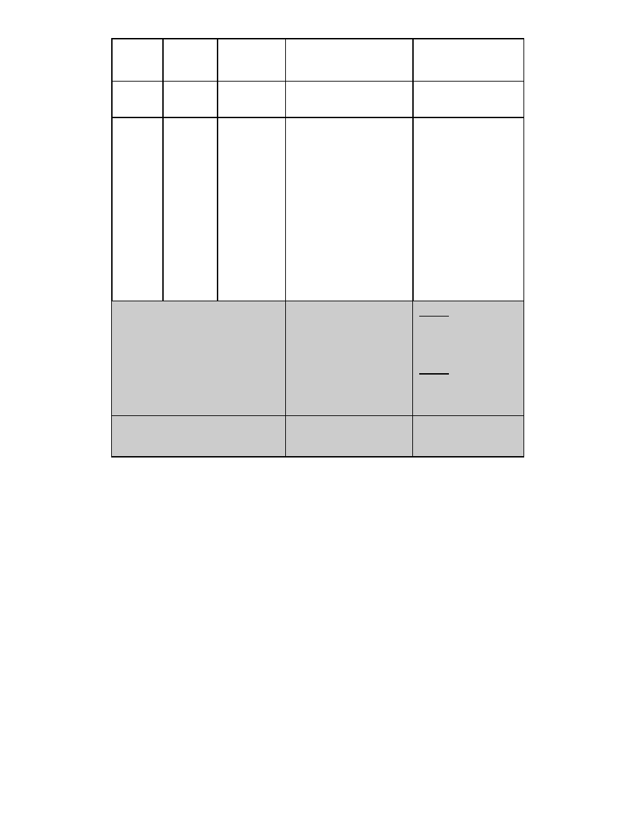
265
Logical
Device
Number
Logical
Device
Register
Index
Base I/O
Range (note3)
Fixed
Base Offsets
+5 : LSR
+6 : MSR
+7 : SCR
0x05
Serial
Port 2
(IR-
USRT)
0x62, 0x63
[0x100:0x0FF8]
ON 8 BYTE
BOUNDARIES
+0 : Register Block N,
address 0
+1 : Register Block N,
address 1
+2 : Register Block N,
address 2
+3 : Register Block N,
address 3
+4 : Register Block N,
address 4
+5 : Register Block N,
address 5
+6 : Register Block N,
address 6
+7 : USRT Master
Control Reg.
0x06
RTC
n/a
Not Relocatable
Fixed Base Address
Bank 0
0x70 : Address
Register
0x71 : Data Register *
Bank 1
0x74 : Address
Register
0x71 : Data Register *
0x07
KYBD
n/a
Not Relocatable
Fixed Base Address
0x60 : Data Register
0x64 :
Command/Status Reg.
Note3 : This chip uses all ISA address bits to decode the base address of each of its logical
devices.
*When these registers are accessed the nNOWS line is not asserted. All other register in this table
assert the nNOWS signal when accessed.

266
Interrupt Select Configuration Register Description
Table 78 -Interrupt Select Configuration Registers
Name
Reg Index
Definition
State
Interrupt
request level
select 0
0x70 (R/W)
Bits[3:0] Selects which interrupt level is used for
Interrupt 0.
0x00=no interrupt selected.
0x01=IRQ1
0x02=IRQ2
o
o
o
0x0E= IRQ14
0x0F= IRQ15
Note: All pin-type interrupts are edge high (except
ECP/EPP). Each Logical Device's interrupts
selected through this register physically select the
interrupts to be used by the FDC37C957FR for either
the Serial IRQ interface or for the individual pin-type
ISA interrupts if selected. Setting the IRQ through
this register for the Parallel Port is not reflected in the
Enhanced Parallel port cnfgB register, software must
set the DMA/IRQ bits in the Parallel Port logical
device config register 0xF1 (Parallel Port CnfgB
shadow register).
Note: It is possible for both UART1 and UART2 to
share a common IRQ pin (refer to Table 80 in the
Logical Device 4 SMC defined Configuration
Registers section).
C
Note :
An Interrupt is activated by Setting the Interrupt Request Level Select 0 register to a non-
zero value AND :
1)
for the FDC logical device by setting DMAEN, bit D3 of the Digital Output Register.
2)
for the PP logical device by setting IRQE, bit D4 of the Control Port and in addition
3)
for the PP logical device in ECP mode by clearing serviceIntr, bit D2 of the ecr.
4)
for the Serial Port logical device by setting any combination of bits D0-D3 in the IER and
by
setting the OUT2 bit in the UART's Modem Control (MCR) Register.
5)
for the RTC by (refer to the RTC section of this spec.)
6)
for the KYBD by (refer to the KYBD controller section of this spec.)
Note:
IRQ pins must tri-state if not used/selected by any Logical Device.
(Refer to Appendix A)

267
DMA Channel Select Configuration Register Description
Table 79 - DMA Channel Select Cofiguration Registers
Name
Reg Index
Definition
State
DMA Channel
select 0
0x74 (R/W)
Bits[2:0] Select the DMA Channel.
0x00=DMA0
0x01=DMA1
0x02=DMA2
0x03=DMA3
0x04-0x07= No DMA active
C
Note :
A DMA channel is activated by
Setting the DMA Channel Select 0 register to [0x00-0x03]
AND :
1) for the FDC logical device by setting DMAEN, bit D3 of the Digital Output Register
2) for the PP logical device in ECP mode by setting dmaEn, bit D3 of the ecr
3) for the UART2 logical device, by setting the DMA Enable bit. Refer to the IrCC specification
Note:
DMAREQ pins must tri-state if not used/selected by any Logical Device.
Refer to Appendix A of this section.

268
SMC Defined Logical Device Configuration Registers
The SMC Specific Logical Device Configuration Registers reset to their default values only on hard
resets generated by VCC2 POR or the RESET_OUT signal. These registers are not effected by Soft
Resets.
Floppy Disk Controller, Logical Device 0 [Logical Device Number = 0x00]
Name
Reg
Index
Definition
State
FDD Mode Register
Default = 0x0E
0xF0 R/W
Bit[0] : Floppy Mode
= 0 Normal Floppy Mode (default)
= 1 Enhanced Floppy Mode 2 (OS2)
Bit[1] : FDC DMA Mode
= 0 Burst Mode is enabled
= 1 Non-burst Mode (default)
Bit[3:2] : Interface Mode
Bit-3 - IDENT
Bit-2 - MFM
= 11 AT Mode (default)
= 10 (Reserved)
= 01 PS/2
= 00 Model 30
Bit[4] : Swap Drives 0,1 Mode
= 0 No swap (default)
= 1 Drive and Motor sel 0 and 1 are
swapped.
Bit[5] : FDC Shutdown
= 0
FDC37C957FR FDC operates
normally, FDC pins are active. (default)
= 1
FDC core is shutdown, only I/O
Writes to DOR, TDR, DSR, and CCR
are enabled, all Floppy Disk interface
pins tri-state except for DRVDEN0,
DRVDEN1, nDS0, nDS1, nMTR0, and
nMTR1. (see the ori_sio.doc
specification for further details).
Bit[6] : FDC Output Type Control
= 0 : FDC Outputs are OD24 Open Drain
(default).
= 1 : FDC Outputs are O24 push pull.
Bit[7] : FDC Output Control
C

269
Name
Reg
Index
Definition
State
= 0 FDC Outputs active (default)
= 1 FDC Outputs tri-stated
Note : Bits 6 and 7 do not effect the Parallel
Port FDC pins.
FDD Option
Register
Default = 0x00
0xF1 R/W
Bits[1:0] : Reserved, set to zero
Bits[3:2] : Density Select
= 00 Normal (default)
= 01 Normal (reserved for users)
= 10 1 (forced to logic "1")
= 11 0 (forced to logic "0")
Bits[5:4] : Media ID Polarity
= 00 (default)
= 01
= 10
= 11
Bits[7:6] : Boot Floppy
= 00 FDD 0 (default)
= 01 FDD 1
= 10 FDD 2
= 11 FDD 3
C
FDD Type Register
Default = 0xFF
0xF2 R/W
Bits[1:0] : Floppy Drive A Type
Bits[3:2] : Floppy Drive B Type
Bits[5:4] : Floppy Drive C Type
Bits[7:6] : Floppy Drive D Type
C
0xF3 R
Reserved, Read as 0 (read only)
C
FDD0
Default = 0x00
0xF4 R/W
Bits[1:0] : Drive Type select
Bits[2] : Read as 0 (read only)
Bits[3:4] : Data Rate Table Select
Bits[5] : Read as 0 (read only)
Bits[6] : Precomp Disable
Bits[7] : Read as 0 (read only)
C
FDD1
0xF5 R/W
Refer to definition and default for 0xF4
C

270
RESERVED, Logical Device 1 [Logical Device Number = 0x01]
RESERVED, Logical Device 2 [Logical Device Number = 0x02]
Parallel Port, Logical Device 3 [Logical Device Number = 0x03]
Name
Reg
Index
Definition
State
PP Mode
Register
Default = 0x3C
0xF0 R/W
Bits[2:0] : Parallel Port Mode
= 100
Printer Mode (default)
= 000
Standard and Bi-directional
(SPP) Mode
= 001
EPP-1.9 and SPP Mode
= 101
EPP-1.7 and SPP Mode
= 010
ECP Mode
= 011
ECP and EPP-1.9 Mode
= 111
ECP and EPP-1.7 Mode
Bit[6:3] : ECP FIFO Threshold
0111b (default)
Bit[7] : PP Interupt Type
Not valid when the parallel port is in the
Printer Mode (100) or the
Standard & Bi-directional Mode (000).
= 1
Pulsed Low, released to high-Z
(665/666).
= 0
IRQ follows nACK when
parallel port in EPP Mode or [Printer,SPP,
EPP] under ECP.
IRQ level type when the parallel
port is in ECP, TEST, or
Centronics FIFO Mode.
C
Parallel Port
CnfgB shadow
Register
Default = 0x00
0xF1 R/W
Bits[2:0] : Parallel Port DMA channel Select
= 000
h/w jumpered 8-bit DMA
(default)
= 001
DMA channel 1
= 010
DMA channel 2
= 011
DMA channel 3
Bits[5:3] : Parallel Port IRQ line Select
= 000
h/w jumpered IRQ (default)
= 001
IRQ 7
C

271
Name
Reg
Index
Definition
State
= 010
IRQ 9
= 011
IRQ 10
= 100
IRQ 11
= 101 IRQ 14
= 110
IRQ 15
= 111
IRQ 5
Bits[7:6] : Reserved, ignores writes
returns 0 on reads.
The DMA/IRQ bits in this register are reflected in
the Enhanced Parallel Port's read only cnfgB
register.
Serial Port 1, Logical Device 4 [Logical Device Number = 0x04]
Name
Reg Index
Definition
State
Serial Port 1
Mode Register
Default = 0x00
0xF0 R/W
Bit[0] : MIDI Mode
= 0 MIDI support disabled (default)
= 1 MIDI support enabled
Bit[1] : High Speed
= 0 High Speed Disabled(default)
= 1 High Speed Enabled
Bit[6:2] : Reserved, set to zero
Bit[7] : Share_IRQ
= 0 UARTS use different IRQs.
= 1 UARTS share a common IRQ.
SeeTable 80.
C

272
Table 80 - UART Shared Interrupt Operation
UART1
UART2
IRQ PINS
UART1
OUT2 bit
UART1
IRQ State
UART2
OUT2 bit
UART2
IRQ State
Share IRQ
Bit
UART1
Pin State
UART2
Pin State
This part of the table is based on the assumption that both UARTS have selected
different IRQ pins.
0
Z
0
Z
0
Z
Z
1
asserted
0
Z
0
1
Z
1
de-
asserted
0
Z
0
0
Z
0
Z
1
asserted
0
Z
1
0
Z
1
de-
asserted
0
Z
0
1
asserted
1
asserted
0
1
1
1
asserted
1
de-
asserted
0
1
0
1
de-
asserted
1
asserted
0
0
1
1
de-
asserted
1
de-
asserted
0
0
0
0
Z
0
Z
1
Z
Z
1
asserted
0
Z
1
1
1
1
de-
asserted
0
Z
1
0
0
0
Z
1
asserted
1
1
1
0
Z
1
de-
asserted
1
0
0
1
asserted
1
asserted
1
1
1
1
asserted
1
de-
asserted
1
1
1
1
de-
asserted
1
asserted
1
1
1
1
de-
asserted
1
de-
asserted
1
0
0
It is the responsibility of the software to ensure that two IRQ's are not set to the same IRQ
number. However, if they are set to the same number than no damage to the chip will result.

273
Serial Port 2, Logical Device 5 [Logical Device Number = 0x05]
Name
Reg
Index
Definition
State
Serial Port 2
Mode Register
Default = 0x00
0xF0 R/W
Bit[0] : MIDI Mode
= 0 MIDI support disabled (default)
= 1 MIDI support enabled
Bit[1] : High Speed
= 0 High Speed Disabled(default)
= 1 High Speed Enabled
Bit[7:2] : Reserved, set to zero
C
IR Option Register
Default = 0x00
This register sets
the IR Options and
uses the same bit
definitions as the
FDC37C93x
0xF1 R/W
Bit[0] : Receive Polarity
= 0 - Active High
= 1 - Active Low (Default)
Bit[1] : Transmit Polarity
= 0 - Active High (Default)
= 1 - Active Low
Bit[2] : Duplex Select
= 0 - Full Duplex (Default)
= 1 - Half Duplex
Bits[5:3] : UART/IR Mode
= 000 - Standard COMM
= 001 IrDA SIR-A
= 010 ASK-IR
= 011 (IrDA SIR-B)
= 100 (IrDA HDLC)
= 101 (IrDA 4PPM)
= 110 (Consumer)
= 111 (Raw IR)
Bits[7:6] : IrCC Output Mux
= 00 : Active Device to
COM-RX/COM-TX port (default).
= 01 : Active Device to IRRX/IRTX
port
= 10 : Reserved -use AUX port not
mapped to pins thus both IR and COM
ports are inactive.
C

274
Name
Reg
Index
Definition
State
= 11 : Reserved, All ports are inactive.
IR Half Duplex
Timeout
Default = 0x03
0xF2 R/W
Bits[7:0]
These bits set the half duplex time-out for the IR
port. This value is 0 to 10ms in 100us
increments.
= 0x00 : blank RX/TX during Transmit/Receive.
= 0x01 : blank RX/TX during Xmit/Rcv + 100us
.....
= 0x64 : blank RX/TX during Xmit/Rcv+ 10ms
= 0x65-0xFF : Reserved
EN_1 : Bits [5:0] of the IR Option Configuration Register must be reconciled with bits[5:0] of the
"USRT Configuration Register A" control register in the IrCC Block, detailed in the IrCC specification.
Additionally Bits [7:6] of the IR Option Configuration Register must be reconciled with bits[5:4] of the
"USRT Configuration Register B" control register in the IrCC Block. The last register written should
update the information in both registers. (both sets of registers can use common latches to store the
information.)
RTC, Logical Device 6 [Logical Device Number = 0x06]
Name
Reg
Index
Definition
State
RTC Mode
Register
Default = 0x00
0xF0 R/W
Bit[0] :
= 1 : Lock CMOS RAM 80-9Fh
Bit[1] :
= 1 : Lock CMOS RAM A0-BFh
Bit[2] :
= 1 : Lock CMOS RAM C0-DFh
Bit[3] :
= 1 : Lock CMOS RAM E0-FE h
Bits[7:4] : Reserved, set to zero
note: Once set, bits[3:0] can not be cleared by a
write; bits[3:0] are cleared on VCC2 Power On
Reset, VCC2 Power Off, or upon a Hard Reset
(RESET_OUT asserted). Once lock bits are set,
both the Host and the 8051 are locked out of
accessing the locked locations as long as VCC1
and VCC2 are active. When VCC2 goes to 0V, the
lock bits are cleared and the 8051 can access the
RAM. The 8051 can access this RAM while
RESET_OUT is asserted.
C

275
KBYD, Logical Device 7 [Logical Device Number = 0x07]
Name
Reg
Index
Definition
State
System-to-8051
Mailbox Register
0x82 R/W
(1)
C, R
8051-to-System
Mailbox Register
0x83 R/W
(1)
C, R
Mailbox Register
2 - F
0x84-0x91
R/W
(1)
C, R
PWM0 Register
0x92 R/W
(1)
C, R
PWM1 Register
0x93 R/W
(1)
C, R
8051STP_CLK
0x94 R/W
(1)
C, R
HMEM
0x95 R/W
(1)
C, R
ESMI source
register
0x96 R/W
(1)
C, R
ESMI mask register
0x97 R/W
(1)
C, R
IR data register
0x98 R/W
(1)
C, R
Force Disk Change
Register
0x99 R/W
See the description of the Force Disk Change
Register in the Floppy Disk Controller Section of
this specification.
C, R
Floppy Data Rate
Select Shadow
Register
0x9A R
See the description of the Floppy Data Rate
Select Register in the Floppy Disk Controller
Section of this specification.
C, R
UART1 FIFO
Control
Shadow Register
0x9B R
This register provides a means of reading
UART1's FIFO Control Register. See the
UART section of this specification.
C, R
UART2 FIFO
Control
Shadow Register
0x9C R
This register provides a means of reading
UART2's FIFO Control Register. See the UART
section of this specification.
C. R
KRST_GA20
0xF0 R/W
Bit[0] : ENAB_P92
= 0 : Port 92 Disabled
= 1 : Port 92 Enabled
Bits[7:0] : Reserved, set to zero.
(1)
Refer to the 8051 Section of this data sheet for descriptions of
these registers.

276
Open Mode Registers
Included here is a concise table
of all of the Open Mode accessible registers on the FDC37C957FR
device. Open Mode registers can be accessed through the chips Open Mode Index and Data
registers and are signified by the prefix IDX in front of their Hexidecimal address.
Table 81 - Open Mode Registers
Open
Mode
Index
Address
Sys-
tem
R/W
8051
address
(7F00 +)
8051
R/W
Power
Source
VCC
1
POR
VCC2
POR
Zero
Wait
State
(1)
Notes
See
Page #
System-
to-8051
Mailbox
register 0
IDX 82h
R/W
08h
RC
VCC1
00
Y
2
192
8051-to-
system
Mailbox
register 1
IDX 83h
RC
09h
R/W
VCC1
00
Y
3
192
Mailbox
register
[2-F]
IDX 84h-
91h
R/W
0A-17h
R/W
VCC1
00h
Y
193
PWM0
register
IDX 92h
R/W
25h
R/W
VCC1
00h
Y
200
PWM1
register
IDX 93h
R/W
26h
R/W
VCC1
00h
Y
200
8051STP
_CLK
IDX 94h
R/W
------
-----
VCC1
00h
Y
5
168
HMEM
IDX 95h
R/W
-----
VCC1
03h
03h
Y
4, 5, 6
166
ESMI
source
register
IDX 96h
R/W
------
-----
VCC2
00h
Y
193
ESMI
mask
register
IDX 97h
R/W
------
-----
VCC2
00h
Y
193
IR data
register
IDX 98h
R/W
------
-----
VCC2
00h
Y
206
Force
Disk
Change
register
IDX99h
R/W
------
-----
VCC2
03h
Y
278
Floppy
Data
Rate
Select
Shadow
register
IDX9A
R
------
-----
VCC2
N/A
Y
278
UART1
FIFO
Control
Shadow
register
IDX9B
R
------
-----
VCC2
00h
Y
-----

277
Open
Mode
Index
Address
Sys-
tem
R/W
8051
address
(7F00 +)
8051
R/W
Power
Source
VCC
1
POR
VCC2
POR
Zero
Wait
State
(1)
Notes
See
Page #
UART2
FIFO
Control
Shadow
register
IDX9C
R
------
-----
VCC2
00h
Y
-----
1) When accessed for a read or write by the System the registers mared with a "Y" will drive the
Zero wait state pin active.
2) Interrupt is cleared when read by the 8051
3) Interrupt is cleared when read by the host
4) DESIGN NOTE: These registers can be on VCC1 or VCC2
5) When IRESET_OUT is cleared (written from "1" to"0") 8051STP_CLK bit D0 as well as HMEM
bits D1 and D0 are all set to "1".
6) These registers are reset 500us to 1ms following the condition that BOTH VCC2 is valid and
PWRGD is asserted given that the RTC is in normal mode and the VRT bit is set (refer to the
RTC section). If the RTC is not in normal mode and/or the VRT bit is not set then these registers
are reset within 10us following the condition that BOTH VCC2 is valid and PWRGD is asserted.
System Shadow Registers
The FDC37C957FR makes the following Control Registers readable by supplying a set of Index
Registers accessable either through Logical Device 7 when in Confuration State or through the Open
Mode Index and Data registers when in Run State.
Sys.
index
Sys
R/W
8051
address
(7F00+)
8051
R/W
Power
Sourc
e
VCC1
POR
VCC2
POR
Zero
Wait
State
(9)
Notes
Force
Diskchange
IDX99
R
------
N/A
VCC2
03h
------
Floppy Data
Rate Select
shadow
register
IDX9A
R
------
N/A
VCC2
N/A
------
UART1 FIFO
Control
Shadow
register
IDX9B
R
------
N/A
VCC2
00h
UART2 FIFO
Control
Shadow
register
IDX9C
R
------
N/A
VCC2
00h

278
Floppy Data Rate Select shadow register
D7
D6
D5
D4
D3
D2
D1
D0
8051
R/W
N/A
N/A
N/A
N/A
N/A
N/A
N/A
N/A
System
R/W
R
R
R
R
R
R
R
R
Bit Def
Soft
Reset
Power
Down
0
PRECOM
P 2
PRECOM
P 1
PRECOM
P 0
Data
Rate
Select 1
Data
Rate
Select 0
Note:
D1 and D0 are updated by a write to the Floppy Data Rate or CCR registers. Bits D7-D2
are updated by a write to the Floppy Data Rate register only.
Force Diskchange
D7-D2
D1
D0
System
R/W
R
R/W
R/W
Bit Def
Reserved
1 = Force a diskchange indication when the DIR register (of the
Floppy controller) is read, gated with Drive Select 0 or 1. These bits
can be written to a "1" but are not clear-able by the software. These
bits are reset when nSTEP input is active with the proper drive
select to the drive occurs. D0 is cleared on nSTEP and Drive Select
0; D1 is cleared on nSTEP and Drive Select 1.
Equivalent logic : when read DIR Bit-7 == (Drive_Sel_0 & D0) OR (Drive_Sel_1 & D1) OR
DSK_CHG

279
Typical Sequence of Configuration Operation
1. At VCC2 power-up, all logical device configuration registers are set to their internal
default state.
2. The chip enters the RUN State, and is ready to be placed into Configuration State.
3. Place the chip into the Configuration State. Once the chip enters into the Configuration State the
auto Config ports are enabled.
4. The system sets the logical device information and activates desired logical devices through the
chips INDEX and DATA ports.
5. The system sends other commands.
6. Exit the Configuration State. The chip returns to the RUN State.
Note :
Only two States are defined (Run and Configuration). In the Run State the chip will always
be ready to enter the Configuration State.

280
APPENDIX A (Configuration Section)
665GT FDC Core Modifications
1. FDC DMA Mode defaults to Non-Burst Mode
2. FDC Core command to handle Density Select function. Implement to simplify support of 3-
Mode drives for users/customers
Drive Rate Table
Data Rate
Data Rate
DENSEL
(1)
DRATE
(1)
DRT1
DRT0
Sel 1
Sel 0
MFM
FM
1
0
0
0
1
1
1Meg
---
1
1
1
0
0
0
0
500
250
1
0
0
0
0
0
1
300
150
0
0
1
0
0
1
0
250
125
0
1
0
0
1
1
1
1Meg
---
1
1
1
0
1
0
0
500
250
1
0
0
0
1
0
1
500
250
0
0
1
0
1
1
0
250
125
0
1
0
1
0
1
1
1Meg
---
1
1
1
1
0
0
0
500
250
1
0
0
1
0
0
1
2Meg
---
0
0
1
1
0
1
0
250
125
0
1
0
Drive Rate Table
(Recommended)
00 = Regular drives and 2.88 vertical format
01 = 3-mode drive
10 = 2 meg tape
(1) DENSEL, DRATE1 and DRATE0 map onto output pins DRVDEN0 and DRVDEN1

281
DT0
DT1
DRVDEN0
(1)
DRVDEN1
(1)
Drive Type
0
0
DENSEL
DRATE0
4/2/1 MB 3.5"
2/1 MB 5.25" FDDS
2/1.6/1 MB 3.5" (3-MODE)
0
1
DRATE1
DRATE0
1
0
nDENSEL
DRATE0
1
1
DRATE0
DRATE1
There are four of the following registers in the configuration data space, one for each drive.
FDD0 - 0xF4
FDD1 - 0xF5
D7
D6
D5
D4
D3
D2
D1
D0
0
PTS
0
DRT1
DRT0
0
DT0
DT1
PTS
= 0 Use Precompensation
= 1 No Precompensation
DTx = Drive Type select
DRTx = Data Rate Table select
(1) DENSEL, DRATE1 and DRATE0 map onto three output pins DRVDEN0 and DRVDEN1.
IRQ and DMA Enable and Disable
Any time the IRQ and/or DMA channel for a logical device is disabled by a register in that logical
device, the IRQ and/or nDACK must be disabled. This is in addition to the IRQ and nDACK disabled
by the Configuration Registers (activate bit cleared or address outside of valid range or the Interrupt
Select register set to 0x00 or the DMA Channel Select register set to 0x04.

282
Logical Device 0 (FDC)
For the following cases, the IRQ and DACK used by the FDC are disabled (high impedance), i.e., will
not respond to the DREQ
1) Digital Output Register (Base+2) bit D3 (DMAEN) set to "0".
2) The FDC is in power down (disabled).
Logical Device 5 (Serial Port1)
Modem Control Register (MCR) Bit D2 (OUT2) - When OUT2 is a logic "0", then the serial port
interrupt is forced to a high impedance state - disabled.
Logical Device 5 (Serial Port2/USART)
Interrupt is disabled when:
Modem Control Register (MCR) bit-2 (OUT2) - When OUT2 is a logic "0", then Logical Device 5's
interrupt is forced to a high impedance state, i.e., disabled. This applies to all UART/IR modes of
operation.
DRQ is disabled when:
USRT Configuration Register B bit-0 (DMA Enable) - When the DMA Enable bit is a logic "0",
then logical device 5's DRQ pin is forced to a high impedance state, i.e., disabled. When the
DMA Enable bit is set to logic "1", then logical device 5's DRQ pin is active and drives low until
the device issues a DMA Request at which point the DRQ pin drives high. This eliminates the
need for an external pull-down resistor on the logical device 5's DRQ pin.

283
Parallel Port
SPP and EPP modes: Control Port (Base+2) bit D4 (IRQE) set to "0", IRQ is disabled (high
impedance).
ECP Mode:
(DMA) dmaEn from ecr register. See table.
IRQ - See table
below.
Mode
(From ecr Register)
IRQ Pin Controlled
By:
PDREQ Pin Controlled
By:
000
PRINTER
IRQE
dmaEn
001
SPP
IRQE
dmaEn
010
FIFO
(on)
dmaEn
011
ECP
(on)
dmaEn
100
EPP
IRQE
dmaEn
101
RES
IRQE
dmaEn
110
TEST
(on)
dmaEn
111
CONFIG
IRQE
dmaEn
Real Time Clock (RTC)
(refer to the RTC section of this spec)
Keyboard Controller (KYBD)
(refer to the Keyboard controller section of this spec)

284
ELECTRICAL SPECIFICATIONS
MAXIMUM GUARANTEED RATINGS *
Operating Temperature Range ........................................................................................ 0
o
C to +70
o
C
Storage Temperature Range .........................................................................................-55
o
to +150
o
C
Lead Temperature Range (soldering, 10 seconds).................................................................... +325
o
C
Positive Voltage on any pin, with respect to Ground ..............................................................V
CC
+0.3V
Negative Voltage on any pin, with respect to Ground................................................................... -0.3V
Maximum V
CC
................................................................................................................................ +7V
*Stresses above those listed above could cause permanent damage to the device. This is a stress
rating only and functional operation of the device at any other condition above those indicated in the
operation sections of this specification is not implied.
Note: When powering this device from laboratory or system power supplies, it is important that the
Absolute Maximum Ratings not be exceeded or device failure can result. Some power supplies
exhibit voltage spikes on their outputs when the AC power is switched on or off. In addition, voltage
transients on the AC power line may appear on the DC output. If this possibility exists, it is
suggested that a clamp circuit be used.
OPERATING CONDITIONS:
Symbol
Parameter
Min
Typ
Max
Units
Vcc0
Vbat for RTC
3.3/4.7
V
Vcc1
Vcc for 8051
4.7
V
Vcc2
System Vcc
5
V
32MHZ_IN
Serial Comm Clock
33
MHZ
XTAL1/XTAL2
RTC Crystal
32.768
KHZ
14.31MHZ_IN
System Clock
14.318
MHZ

285
POWER DISTRIBUTION:
Type 1 Device
VCC0, "Vbat" (RTC)
VCC1 (8051 + other)
VCC2 (SI/O)
0 volts
0 volts
0 volts
Powerdown <20ua
4.7 volts
4.7 volts
0 volts
Run on 4 Mhz
4.7 volts
4.7 volts
0 volts
Run on 4 Mhz
4.7 volts
4.7 volts
5 volts
14 Meg input
4.7 volts
4.7 volts
5 volts
Type 2 Device
VCC0, "Vbat" (RTC)
VCC1 (8051 + other)
VCC2 (SI/O)
0 volts
0 volts
0 volts
RTC only <1ua
3.3 volts
0 volts
0 volts
Powerdown <20ua
4.7 volts
4.7 volts
0 volts
Run on 4 Mhz
4.7 volts
4.7 volts
0 volts
Run on 4 Mhz
4.7 volts
4.7 volts
5 volts
14 Meg input
4.7 volts
4.7 volts
5 volts
VCC2 < 3.7V ; lock-out host
VCC1 < 2.5V ; lock-out 8051
Type 1 Device:
Vcc0 & Vcc1 tied together and sourced by main battery supply.
Type 2 Device:
Vcc0 connected to Vbat.
Vcc1 connected to main battery supply.
Vcc2 is switched supply from either main battery or AC if plugged in.

286
DC SPECIFICATIONS
DC ELECTRICAL CHARACTERISTICS (T
A
= 0∞C - 70∞C, V
CC
= +5.0 V ± 10%)
PARAMETER
SYMBOL
MIN
TYP
MAX
UNITS
COMMENTS
I Type Input Buffer
Low Input Level
High Input Level
V
ILI
V
IHI
2.0
0.8
V
V
TTL Levels
IS Type Input Buffer
Low Input Level
High Input Level
Schmitt Trigger
Hysteresis
V
ILIS
V
IHIS
V
HYS
2.2
250
0.8
V
V
mV
Schmitt Trigger
Schmitt Trigger
ISP Type Input Buffer
with 90
µ
A weak pull-up
Low Input Level
High Input Level
Schmitt Trigger
Hysteresis
V
ILIS
V
IHIS
V
HYS
2.2
250
0.8
V
V
mV
Schmitt Trigger
Schmitt Trigger
I
CLK
Input Buffer
Low Input Level
High Input Level
V
ILCK
V
IHCK
3.0
0.4
V
V
O
CLK2
Crystal Oscillator
Output
I
CLK2
Crystal Oscillator
Input
Use a 32 KHz parallel resonant crystal oscillator. The load
capacitors are seen by the crystal as two capacitors in series
and should be approximately 2 times the Co
of the actual
crystal used (C1=2Co). For example, a 7.5pF crystal should
use two 15pF capacitors for proper loading. The 1 Meg reg
resistor (see .6
µ
A TLM) creates a very low current to bias the
XTAL1 input to ground and shunt any extraneous DC offset.

287
PARAMETER
SYMBOL
MIN
TYP
MAX
UNITS
COMMENTS
Input Leakage
(All I and IS buffers
except PWRGD &
VCC1_PWRGD)
Low Input Leakage
High Input Leakage
I
IL
I
IH
-10
-10
+10
+10
µ
A
µ
A
V
IN
= 0
V
IN
= V
CC
Input Current
PWRGD
I
OH
75
150
mA
V
IN
= 0
O4 Type Buffer
Low Output Level
High Output Level
Output Leakage
V
OL
V
OH
I
OL
2.4
-10
0.4
+10
V
V
µ
A
I
OL
= 4 mA
I
OH
= -2 mA
V
IN
= 0 to V
CC
OD4 Type Buffer
Low Output Level
Output Leakage
V
OL
I
OH
-10
0.4
+10
V
µ
A
V
OL
= 4 mA
I
OH
= 0 to V
CC
O8 Type Buffer
Low Output Level
High Output Level
Output Leakage
V
OL
V
OH
I
OL
2.4
-10
0.4
+10
V
V
µ
A
I
OL
= 8 mA
I
OH
= -4 mA
V
IN
= 0 to V
CC
OD8 Type Buffer
Low Output Level
Output Leakage
V
OL
I
OH
-10
0.4
+10
V
µ
A
V
OL
= 8 mA
I
OH
= 0 to V
CC
O24 Type Buffer
Low Output Level
High Output Level
Output Leakage
V
OL
V
OH
I
OL
2.4
-10
0.4
+10
V
V
mA
I
OL
= 24 mA
I
OH
= -12 mA
V
IN
= 0 to V
CC

288
PARAMETER
SYMBOL
MIN
TYP
MAX
UNITS
COMMENTS
OD24 Type Buffer
Low Output Level
High Output Level
Output Leakage
V
OL
V
OH
I
OL
2.4
-10
0.4
+10
V
V
mA
I
OL
= 24 mA
I
OH
= -50 mA
V
IN
= 0 to V
CC
Supply Current Active
Supply Current Standby
I
CC
I
CSBY
TBD
TBD
TBD
mA
µ
A
All outputs
open.
AC SPECIFICATIONS
AC TEST CONDITIONS
CAPACITANCE T
A
= 25∞C; fc = 1MHz; V
CC
= 5V
PARAMETER
SYMBOL
LIMITS
UNIT
TEST CONDITION
MIN
TYP
MAX
Clock Input
Capacitance
C
IN
20
pF
All pins except pin
under test tied to AC
ground
Input Capacitance
C
IN
10
pF
Output Capacitance
C
OUT
20
pF

289
TIMING DIAGRAMS
Load Capacitance
For the Timing Diagrams shown, the following capacitive loads are used.
Table 82 - Capacitive Loading
NAME
CAPACITANCE
TOTAL (pF)
NAME
CAPACITANCE
TOTAL (pF)
SD[0:7]
240
nALF
240
IOCHRDY
240
nSTB
240
IRQ[1,3,4, 6-8, 12]
120
EMCLK
240
nSMI
120
EMDAT
240
DRQ[0:1]
120
IMCLK
240
32KHz_OUT
50
IMDAT
240
24MHz_OUT
50
KBDAT
240
nWGATE
240
KBCLK
240
nWDATA
240
PS2DAT
240
nHDSEL
240
PS2CLK
240
nDIR
240
nNOWS
240
nSTEP
240
FAD[0:7]
100
nDS[1:0]
240
FA[8:17]
100
nMTR[1:0]
240
nFRD
50
DRVDEN[1:0]
240
nFWR
50
TXD1
100
FALE
50
nRTS1
100
KSO[0:13]
100
nDTR1
100
SIRQ
150
TXD2
100
FPD
50
nRTS2
100
AB_DATA
100
nDTR2
100
AB_CLK
100
PD[0:7]
240
IRTX
50
nSLCTIN
240
PWM[0:1]
50
nINIT
240
nRESET_OUT
240

290
Diagrams
t3
t4
t1
t2
t5
SA[x]
SD[7:0]
nIOW
Figure 19 - FASTGATEA20 IOW TIMING
In order to use the FastGATEA20 speed-up mechanism, data must be available by the
falling edge of nIOW.
Table 83 - FastGATEA20 IOW Timing Parameters
NAME
DESCRIPTION
MIN
TYP
MAX
UNITS
t1
SA[x] Valid to nIOW Asserted
10
ns
t2
SD[7:0] Valid to nIOW Asserted
0
ns
t3
nIOW Asserted to SA[x] Invalid
10
ns
t4
nIOW Deasserted to SD[7:0] Invalid
0
ns
t5
nIOW Deasserted to nIOW or nIOR Asserted
100
ns

291
t10
t3
t1
t2
t4
t6
t5
t7
t8
t9
D A T A V A L I D
AEN
SA[x]
nIOW
SD[x]
FINTER
PINTER
IBF
FIGURE 20 - ISA IO WRITE
Table 84 - ISA IO Write Parameters
NAME
DESCRIPTION
MIN
TYP
MAX
UNITS
t1
SA[x] and AEN valid to nIOW asserted
10
ns
t2
nIOW asserted to nIOW deasserted
80
ns
t3
nIOW asserted to SA[x] invalid
10
ns
t4
SD[x] Valid to nIOW deasserted
45
ns
t5
SD[x] Hold from nIOW deasserted
0
ns
t6
nIOW deasserted to nIOW asserted
25
ns
t7
nIOW deasserted to FINTR deasserted (Note 1)
55
ns
t8
nIOW deasserted to PINTER deasserted (Note 2)
260
ns
t9
IBF (internal signal) asserted from nIOW deasserted
40
ns
t10
nIOW deasserted to AEN invalid
10
ns
Note 1: FINTR refers to the IRQ used by the floppy disk logical device.
Note 2: PINTR refers to the IRQ used by the parallel port logical device.

292
t13
t3
t1
t7
t2
t6
t4
t5
t10
t9
t11
t12
t8
DATA VALID
AEN
SA[x]
nIOR
SD[x]
PD[x], nERROR,
PE, SLCT, ACK, BUSY
FINTER
PINTER
PCOBF
AUXOBF1
nIOR/nIOW
FIGURE 21 - ISA IO READ CYCLE

293
Table 85 - ISA IO Read Timing Parameters
NAME
DESCRIPTION
MIN
TYP
MAX
UNITS
t1
SA[x] and AEN valid to nIOR asserted
10
ns
t2
nIOR asserted to nIOR deasserted
50
ns
t3
nIOR asserted to SA[x] invalid
10
ns
t4
nIOR asserted to Data Valid
50
ns
t5
Data Hold/float from nIOR deasserted
10
25
ns
t6
nIOR deasserted to nIOR asserted
25
ns
t8
nIOR asserted after nIOW deasserted
80
ns
t8
nIOR/nIOR, nIOW/nIOW transfers from/to ECP
FIFO
150
ns
t7
Parallel Port setup to nIOR asserted
20
ns
t9
nIOR asserted to PINTER deasserted
55
ns
t10
nIOR deasserted to FINTER deasserted
260
ns
t11
nIOR deasserted to PCOBF deasserted (Notes
3,5)
80
ns
t12
nIOR deasserted to AUXOBF1 deasserted (Notes
4,5)
80
ns
t13
nIOR deasserted to AEN invalid
10
ns
Note 1: FINTR refers to the IRQ used by the floppy disk.
Note 2: PINTR refers to the IRQ used by the parallel port.
Note 3: PCOBF is used for the Keyboard IRQ.
Note 4: AUXOBF1 is used for the Mouse IRQ.
Note 5: Applies only if deassertion is performed in hardware.

294
t2
t1
t2
CLOCKI
FIGURE 22 - INPUT CLOCK TIMING
Table 86 - Input Clock Timing Parameters
NAME
DESCRIPTION
MIN
TYP
MAX
UNITS
t1
Clock Cycle Time for 14.318MHZ
65
ns
t2
Clock High Time/Low Time for 14.318MHz
25
ns
t
r
, t
f
Clock Rise Time/Fall Time (not shown)
5
ns

295
t15
t2
t3
t12
t16
t1
t4
t5
t6
t11
t14
t8
t7
t9
t10
t13
AEN
FDRQ,
PDRQ
nDACK
nIOR
or
nIOW
DATA
(DO-D7)
TC
DATA VALID
FIGURE 23 - DMA TIMING (SINGLE TRANSFER MODE)
Table 87 - DMA Timing (Single Transfer Mode) Parameters
NAME
DESCRIPTION
MIN
TYP
MAX
UNITS
t1
nDACK Delay Time from FDRQ High
0
ns
t2
DRQ Reset Delay from nIOR or nIOW
100
ns
t3
FDRQ Reset Delay from nDACK Low
100
ns
t4
nDACK Width
150
ns
t5
nIOR Delay from FDRQ High
0
ns
t6
nIOW Delay from FDRQ High
0
ns
t7
Data Access Time from nIOR Low
100
ns
t8
Data Set Up Time to nIOW High
40
ns
t9
Data to Float Delay from nIOR High
10
60
ns
t10
Data Hold Time from nIOW High
10
ns
t11
nDACK Set Up to nIOW/nIOR Low
5
ns
t12
nDACK Hold after nIOW/nIOR High
10
ns
t13
TC Pulse Width
60
ns
t14
AEN Set Up to nIOR/nIOW
40
ns
t15
AEN Hold from nDACK
10
ns
t16
TC Active to PDRQ Inactive
100
ns

296
t15
t2
t3
t12
t16
t1
t4
t5
t6
t11
t14
t8
t7
t9
t10
t13
AEN
FDRQ,
PDRQ
nDACK
nIOR
or
nIOW
DATA
(DO-D7)
TC
DATA VALID
DATA VALID
FIGURE 24 - DMA TIMING (BURST TRANSFER MODE)
Table 88 - DMA Timing (Burst Transfer Mode) Parameters
NAME
DESCRIPTION
MIN
TYP
MAX
UNITS
t1
nDACK Delay Time from FDRQ High
0
ns
t2
DRQ Reset Delay from nIOR or nIOW
100
ns
t3
FDRQ Reset Delay from nDACK Low
100
ns
t4
nDACK Width
150
ns
t5
nIOR Delay from FDRQ High
0
ns
t6
nIOW Delay from FDRQ High
0
ns
t7
Data Access Time from nIOR Low
100
ns
t8
Data Set Up Time to nIOW High
40
ns
t9
Data to Float Delay from nIOR High
10
60
ns
t10
Data Hold Time from nIOW High
10
ns
t11
nDACK Set Up to nIOW/nIOR Low
5
ns
t12
nDACK Hold after nIOW/nIOR High
10
ns
t13
TC Pulse Width
60
ns
t14
AEN Set Up to nIOR/nIOW
40
ns
t15
AEN Hold from nDACK
10
ns
t16
TC Active to PDRQ Inactive
100
ns

297
t3
t1
t2
t4
t5
t6
t7
t8
t9
t9
nDIR
nSTEP
nDS0-3
nINDEX
nRDATA
nWDATA
nIOW
nDS0-3,
MTR0-3
FIGURE 25 - FLOPPY DISK DRIVE TIMING (AT MODE)
Table 89 - Floppy Disk Drive Timaing (AT Mode) Parameters
NAME
DESCRIPTION
MIN
TYP
MAX
UNITS
t1
nDIR Set Up to STEP Low
4
X*
t2
nSTEP Active Time Low
24
X*
t3
nDIR Hold Time after nSTEP
96
X*
t4
nSTEP Cycle Time
132
X*
t5
nDS0-3 Hold Time from nSTEP Low
20
X*
t6
nINDEX Pulse Width
2
X*
t7
nRDATA Active Time Low
40
ns
t8
nWDATA Write Data Width Low
.5
Y*
t9
nDS0-3, MTRO-3 from End of nIOW
25
ns
*X specifies one MCLK period and Y specifies one WCLK period.
MCLK = Controller Clock to FDC
WCLK = 2 x Data Rate

298
t1
t5
t2
t4
t6
t3
nIOW
nRTSx,
nDTRx
IRQx
nCTSx,
nDSRx,
nDCDx
IRQx
nIOW
IRQx
nIOR
nRIx
FIGURE 26 - SERIAL PORT TIMING
Table 90 - Serial Port Timing Parameters
NAME
DESCRIPTION
MIN
TYP
MAX
UNITS
t1
nRTSx, nDTRx Delay from nIOW
200
ns
t2
IRQx Active Delay from nCTSx, nDSRx, nDCDx
100
ns
t3
IRQx Inactive Delay from nIOR (Leading Edge)
120
ns
t4
IRQx Inactive Delay from nIOW (Trailing Edge)
125
ns
t5
IRQx Inactive Delay from nIOW
10
100
ns
t6
IRQx Active Delay from nRIx
100
ns

299
t1
t4
t3
t2
t2
t5
t3
nIOW
nINIT, nSTROBE.
nAUTOFD, SLCTIN
nACK
PINTR
(ECP or EPP Enabled)
nFAULT (ECP)
nERROR
(ECP)
PINTR
PD0- PD7
t6
nPINTR
(SPP)
FIGURE 27 - PARALLEL PORT TIMING
Table 91 - Parallel Port Timing Parameters
NAME
DESCRIPTION
MIN
TYP
MAX
UNITS
t1
PD0-7, nINIT, nSTROBE, nAUTOFD Delay from
nIOW
100
ns
t2
PINTR Delay from nACK, nFAULT
60
ns
t3
PINTR Active Low in ECP and EPP Modes
200
300
ns
t4
PINTR Delay from nACK
105
ns
t5
nERROR Active to PINTR Active
105
ns
t6
PD0 - PD7 Delay from IOW Active
100
ns

300
t18
t9
t8
t17
t12
t19
t10
t11
t13
t20
t22
t2
t1
t5
t3
t14
t16
t4
t6
t15
t7
t21
A0-A10
SD<7:0>
nIOW
IOCHRDY
nWRITE
PD<7:0>
nDATAST
nADDRSTB
nWAIT
PDIR
FIGURE 28 - EPP 1.9 DATA OR ADDRESS WRITE CYCLE

301
Table 92 - EPP 1.9 Data or Address Write Parameters
NAME
DESCRIPTION
MIN
TYP
MAX
UNITS
t1
nIOW Asserted to PDATA Valid
0
50
ns
t2
nWAIT Asserted to nWRITE Change (Note 1)
60
185
ns
t3
nWRITE to Command Asserted
5
35
ns
t4
nWAIT Deasserted to Command Deasserted
(Note 1)
60
190
ns
t5
nWAIT Asserted to PDATA Invalid (Note 1)
0
ns
t6
Time Out
10
12
ms
t7
Command Deasserted to nWAIT Asserted
0
ns
t8
SDATA Valid to nIOW Asserted
10
ns
t9
nIOW Deasserted to DATA Invalid
0
ns
t10
nIOW Asserted to IOCHRDY Asserted
0
24
ns
t11
nWAIT Deasserted to IOCHRDY Deasserted
(Note 1)
60
160
ns
t12
IOCHRDY Deasserted to nIOW Deasserted
10
ns
t13
nIOW Asserted to nWRITE Asserted
0
70
ns
t14
nWAIT Asserted to Command Asserted (Note 1)
60
210
ns
t15
Command Asserted to nWAIT Deasserted
0
10
ms
t16
PDATA Valid to Command Asserted
10
ns
t17
Ax Valid to nIOW Asserted
40
ns
t18
nIOW Asserted to Ax Invalid
10
ns
t19
nIOW Deasserted to nIOW or nIOR Asserted
40
ns
t20
nWAIT Asserted to nWRITE Asserted (Note 1)
60
185
ns
t21
nWAIT Asserted to PDIR Low
0
ns
t22
PDIR Low to nWRITE Asserted
0
ns
Note 1: nWAIT must be filtered to compensate for ringing on the parallel bus cable. WAIT is
considered to have settled after it does not transition for a minimum of 50 nsec.

302
t20
t19
t11
t22
t13
t12
t8
t10
t18
t23
t24
t27
t9
t21
t17
t2
t25
t5
t4
t16
t1
t14
t26
t28
t3
t7
t15
t6
PData bus driven
by peripheral
A0-A10
IOR
SD<7:0>
IOCHRDY
PDIR
nWRITE
PD<7:0>
DATASTB
ADDRSTB
nWAIT
FIGURE 29 - EPP 1.9 DATA OR ADDRESS READ CYCLE

303
Table 93 - EPP 1.9 Data or Address Read Cycle Timing Parameters
NAME
DESCRIPTION
MIN
TYP
MAX
UNITS
t1
PDATA Hi-Z to Command Asserted
0
30
ns
t2
nIOR Asserted to PDATA Hi-Z
0
50
ns
t3
nWAIT Deasserted to Command Deasserted
(Note 1)
60
180
ns
t4
Command Deasserted to PDATA Hi-Z
0
ns
t5
Command Asserted to PDATA Valid
0
ns
t6
PDATA Hi-Z to nWAIT Deasserted
0
ms
t7
PDATA Valid to nWAIT Deasserted
0
ns
t8
nIOR Asserted to IOCHRDY Asserted
0
24
ns
t9
nWRITE Deasserted to nIOR Asserted (Note 2)
0
ns
t10
nWAIT Deasserted to IOCHRDY Deasserted
(Note 1)
60
160
ns
t11
IOCHRDY Deasserted to nIOR Deasserted
0
ns
t12
nIOR Deasserted to SDATA Hi-Z (Hold Time)
0
40
ns
t13
PDATA Valid to SDATA Valid
0
75
ns
t14
nWAIT Asserted to Command Asserted
0
195
ns
t15
Time Out
10
12
ms
t16
nWAIT Deasserted to PDATA Driven (Note 1)
60
190
ns
t17
nWAIT Deasserted to nWRITE Modified (Notes 1,2)
60
190
ns
t18
SDATA Valid to IOCHRDY Deasserted (Note 3)
0
85
ns
t19
Ax Valid to nIOR Asserted
40
ns
t20
nIOR Deasserted to Ax Invalid
10
10
ns
t21
nWAIT Asserted to nWRITE Deasserted
0
185
ns
t22
nIOR Deasserted to nIOW or nIOR Asserted
40
ns
t23
nWAIT Asserted to PDIR Set (Note 1)
60
185
ns
t24
PDATA Hi-Z to PDIR Set
0
ns
t25
nWAIT Asserted to PDATA Hi-Z (Note 1)
60
180
ns
t26
PDIR Set to Command
0
20
ns
t27
nWAIT Deasserted to PDIR Low (Note 1)
60
180
ns
t28
nWRITE Deasserted to Command
1
ns
Note 1: nWAIT is considered to have settled after it does not transition for a minimum of 50 ns.
Note 2: When not executing a write cycle, EPP nWRITE is inactive high.
Note 3: 85 is true only if t7 = 0.
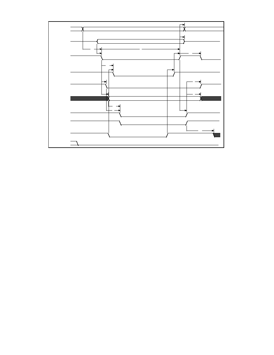
304
t18
t9
t8
t17
t6
t12
t19
t10
t20
t11
t13
t2
t1
t5
t3
t16
t4
t21
A0-A10
SD<7:0>
nIOW
IOCHRDY
nWRITE
PD<7:0>
nDATAST
nADDRSTB
nWAIT
PDIR
FIGURE 30 - EPP 1.7 DATA OR ADDRESS WRITE CYCLE

305
Table 94 - EPP 1.7 Data or Address Write Cycle Timing Parameters
NAME
DESCRIPTION
MIN
TYP
MAX
UNITS
t1
nIOW Asserted to PDATA Valid
0
50
ns
t2
Command Deasserted to nWRITE Change
0
40
ns
t3
nWRITE to Command
5
35
ns
t4
nIOW Deasserted to Command Deasserted (Note 2)
50
ns
t5
Command Deasserted to PDATA Invalid
50
ns
t6
Time Out
10
12
ms
t8
SDATA Valid to nIOW Asserted
10
ns
t9
nIOW Deasserted to DATA Invalid
0
ns
t10
nIOW Asserted to IOCHRDY Asserted
0
24
ns
t11
nWAIT Deasserted to IOCHRDY Deasserted
40
ns
t12
IOCHRDY Deasserted to nIOW Deasserted
10
ns
t13
nIOW Asserted to nWRITE Asserted
0
50
ns
t16
PDATA Valid to Command Asserted
10
35
ns
t17
Ax Valid to nIOW Asserted
40
ns
t18
nIOW Deasserted to Ax Invalid
10
ms
t19
nIOW Deasserted to nIOW or nIOR Asserted
100
ns
t20
nWAIT Asserted to IOCHRDY Deasserted
45
ns
t21
Command Deasserted to nWAIT Deasserted
0
ns
Note 1: nWRITE is controlled by clearing the PDIR bit to "0" in the control register
before performing an EPP Write.
Note 2: The number is only valid if nWAIT is active when IOW goes active.
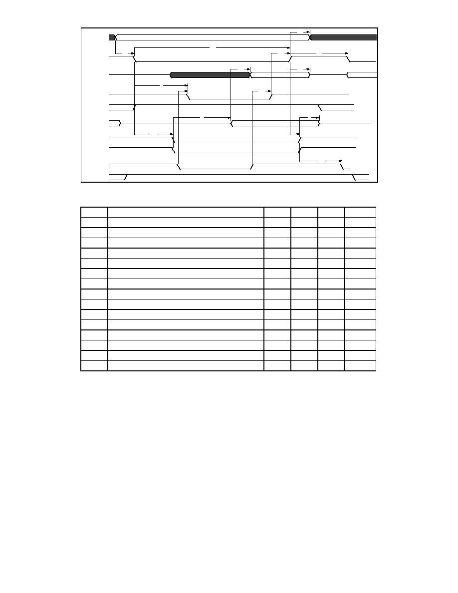
306
t20
t19
t11
t15
t22
t13
t12
t3
t8
t10
t5
t4
t23
t2
t21
A0-A10
nIOR
SD<7:0>
IOCHRDY
nWRITE
PD<7:0>
nDATASTB
nADDRSTB
nWAIT
PDIR
FIGURE 31 - EPP 1.7 DATA OR ADDRESS READ CYCLE
Table 95 - EPP 1.7 Data or Address Read Cycle Timing Parameters
NAME
DESCRIPTION
MIN
TYP
MAX
UNITS
t2
nIOR Deasserted to Command Deasserted
50
ns
t3
nWAIT Asserted to IOCHRDY Deasserted
0
40
ns
t4
Command Deasserted to PDATA Hi-Z
0
ns
t5
Command Asserted to PDATA Valid
0
ns
t8
nIOR Asserted to IOCHRDY Asserted
24
ns
t10
nWAIT Deasserted to IOCHRDY Deasserted
50
ns
t11
IOCHRDY Deasserted to nIOR Deasserted
0
ns
t12
nIOR Deasserted to SDATA High-Z (Hold Time)
0
40
ns
t13
PDATA Valid to SDATA Valid
40
ns
t15
Time Out
10
12
ms
t19
Ax Valid to nIOR Asserted
40
ns
t20
nIOR Deasserted to Ax Invalid
10
ns
t21
Command Deasserted to nWAIT Deasserted
0
ns
t22
nIOR Deasserted to nIOW or nIOR Asserted
40
ns
t23
nIOR Asserted to Command Asserted
55
ns
Note:
WRITE is controlled by setting the PDIR bit to "1" in the control register before
performing an EPP Read.

307
ECP PARALLEL PORT TIMING
Parallel Port FIFO (Mode 101)
The standard parallel port is run at or near the peak 500Kbytes/sec allowed in the forward direction
using DMA. The state machine does not examine nACK, but begins the next transfer based on
Busy. Refer to figure 32.
ECP Parallel Port Timing
The timing is designed to allow operation at approximately 2.0 Mbytes/sec over a 15ft cable. If a
shorter cable is used then the bandwidth will increase.
Forward-Idle
When the host has no data to send it keeps HostClk () high and the peripheral will leave PeriphClk
(Busy) low.
Forward Data Transfer Phase
The interface transfers data and commands from the host to the peripheral using an interlocked
PeriphAck and HostClk. The peripheral may indicate its desire to send data to the host by asserting
nPeriphRequest.
The Forward Data Transfer Phase may be entered from the Forward-Idle Phase. While in the
Forward Phase the peripheral may asynchronously assert the nPeriphRequest (nFault) to request that
the channel be reversed. When the peripheral is not busy it sets PeriphAck (Busy) low. The host then
sets HostClk (nStrobe) low when it is prepared to send data. The data must be stable for the
specified setup time prior to the falling edge of HostClk. The peripheral then sets PeriphAck (Busy)
high to acknowledge the handshake. The host then sets HostClk (nStrobe) high. The peripheral then
accepts the data and sets PeriphAck (Busy) low, completing the transfer. This sequence is shown in
figure 33.
The timing is designed to provide 3 cable round-trip times for data setup if Data is driven simul-
taneously with HostClk (nStrobe).
Reverse-Idle Phase - The peripheral has no data to send and keeps PeriphClk high. The host is idle
and keeps HostAck low.
Reverse Data Transfer Phase - The interface transfers data and commands from the peripheral to the
host using an interlocked HostAck and PeriphClk.
The Reverse Data Transfer Phase may be entered from the Reverse-Idle Phase. After the previous
byte has beed accepted the host sets HostAck (nALF) low. The peripheral then sets PeriphClk
(nACK) low when it has data to send. The data must be stable for the specified setup time prior to the
falling edge of PeriphClk. When the host is ready it to accept a byte it sets HostAck (nALF) high to
acknowledge the handshake. The peripheral then sets PeriphClk (nACK) high. After the host has
accepted the data it sets HostAck (nALF) low, completing the transfer. This sequence is shown in
figure 34.

308
Output Drivers
To facilitate higher performance data transfer, the use of balanced CMOS active drivers for critical
signals (Data, HostAck, HostClk, PeriphAck, PeriphClk) are used ECP Mode. Because the use of
active drivers can present compatibility problems in Compatible Mode (the control signals, by
tradition, are specified as open-collector), the drivers are dynamically changed from open-collector
to totem-pole. The timing for the dynamic driver change is specified in the IEEE 1284
Extended Capabilities Port Protocol and ISA Interface Standard, Rev. 1.14, July 14, 1996,
available from Microsoft. The dynamic driver change must be implemented properly to prevent
glitching the outputs.
t 3
t 6
t 1
t 2
t 5
t 4
P D A T A
n S T R O B E
B U S Y
FIGURE 32 - PARALLEL PORT FIFO TIMING
Table 96 - Parallel Port FIFO Timing Parameters
NAME
DESCRIPTION
MIN
TYP
MAX
UNITS
t1
DATA Valid to nSTROBE Active
600
ns
t2
nSTROBE Active Pulse Width
600
ns
t3
DATA Hold from nSTROBE Inactive (Note 1)
450
ns
t4
nSTROBE Active to BUSY Active
500
ns
t5
BUSY Inactive to nSTROBE Active
680
ns
t6
BUSY Inactive to PDATA Invalid (Note 1)
80
ns
Note 1: The data is held until BUSY goes inactive or for time t3, whichever is longer. This
only applies if another data transfer is pending. If no other data transfer is pending,
the data is held indefinitely.
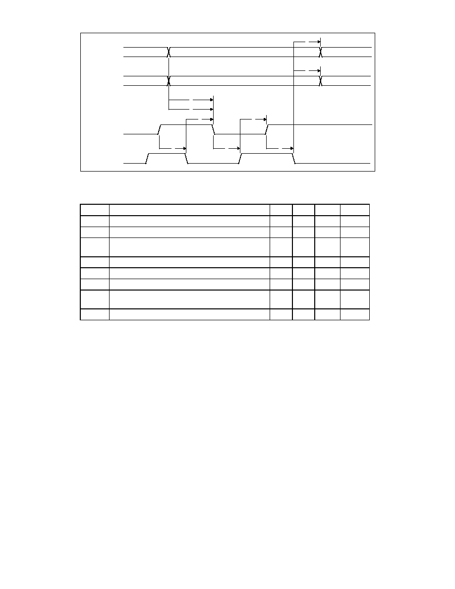
309
t3
t4
t1
t2
t7
t8
t6
t5
t6
nAUTOFD
PDATA<7:0>
BUSY
nSTROBE
FIGURE 33 - ECP PARALLEL PORT FORWARD TIMING
Table 97 - ECP Parallel Port Forward Timing Parameters
NAME
DESCRIPTION
MIN
TYP
MAX
UNITS
t1
nAUTOFD Valid to nSTROBE Asserted
0
60
ns
t2
PDATA Valid to nSTROBE Asserted
0
60
ns
t3
BUSY Deasserted to nAUTOFD Changed
(Notes 1,2)
80
180
ns
t4
BUSY Deasserted to PDATA Changed (Notes 1,2)
80
180
ns
t5
nSTROBE Deasserted to Busy Asserted
0
ns
t6
nSTROBE Deasserted to Busy Deasserted
0
ns
t7
BUSY Deasserted to nSTROBE Asserted
(Notes 1,2)
80
200
ns
t8
BUSY Asserted to nSTROBE Deasserted (Note 2)
80
180
ns
Note 1: Maximum value only applies if there is data in the FIFO waiting to be written out.
Note 2: BUSY is not considered asserted or deasserted until it is stable for a minimum of
75 to 130 ns.

310
t2
t1
t5
t6
t4
t3
t4
PDATA<7:0>
nACK
nAUTOFD
FIGURE 34 - ECP PARALLEL PORT REVERSE TIMING
Table 98 - ECP Parallel Port Reverse Timing
NAME
DESCRIPTION
MIN
TYP
MAX
UNITS
t1
PDATA Valid to nACK Asserted
0
ns
t2
nAUTOFD Deasserted to PDATA Changed
0
ns
t3
nACK Asserted to nAUTOFD Deasserted
(Notes 1,2)
80
200
ns
t4
nACK Deasserted to nAUTOFD Asserted (Note 2)
80
200
ns
t5
nAUTOFD Asserted to nACK Asserted
0
ns
t6
nAUTOFD Deasserted to nACK Deasserted
0
ns
Note 1: Maximum value only applies if there is room in the FIFO and terminal count has not
been received. ECP can stall by keeping nAUTOFD low.
Note 2: nACK is not considered asserted or deasserted until it is stable
for a minimum of 75 to 130
ns.
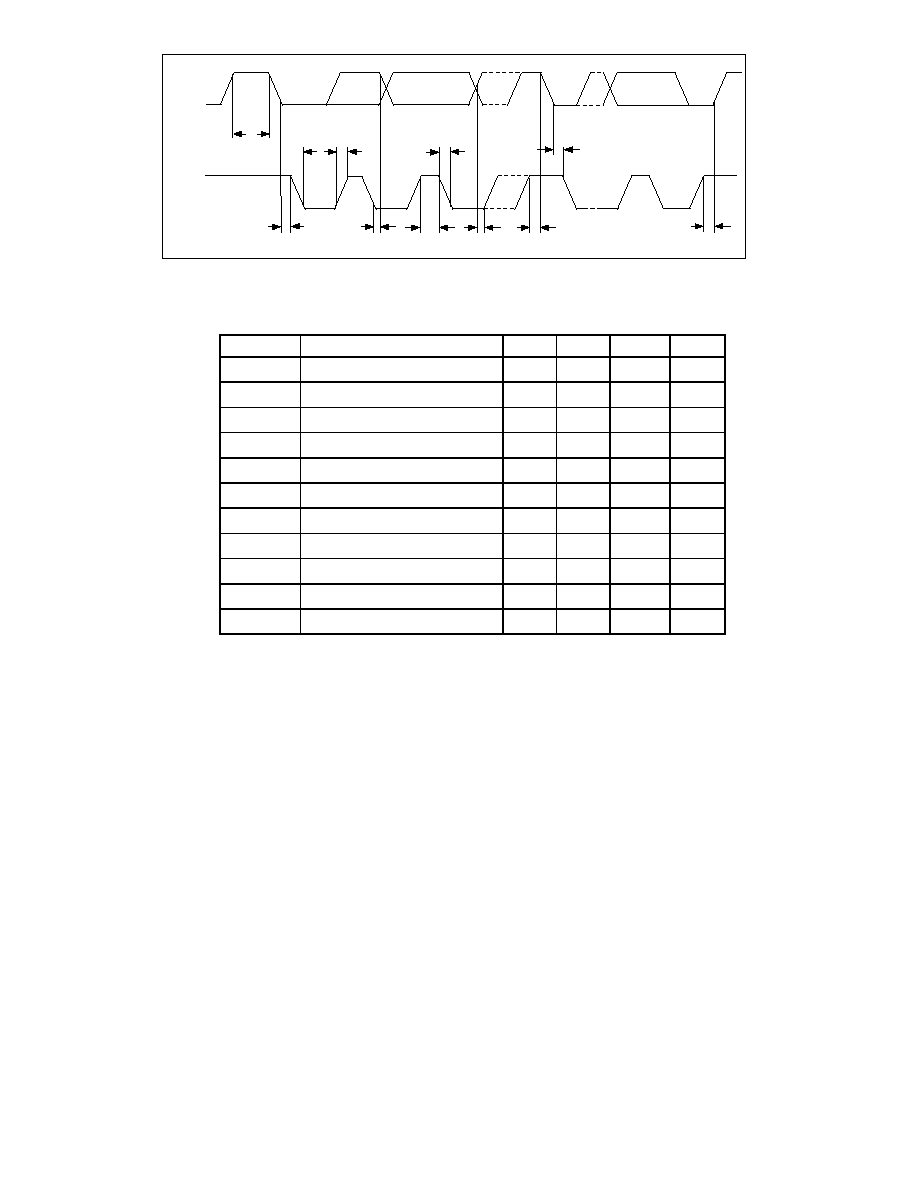
311
t
HD;STA
t
SU;STO
t
SU;STA
t
SU;DAT
t
HIGH
t
F
t
R
t
LOW
t
HD;DAT
t
HD;STA
t
BUF
AB_DATA
AB_CLK
FIGURE 35 - ACESS.BUS TIMING
Table 99 - Access.Bus Timing Parameters
SYMBOL
PARAMETER
MIN.
TYP.
MAX.
UNIT
f
SCL
SCL clock frequency
-
-
100
kHz
t
BUF
Bus free time
4.7
-
-
µs
t
SU;STA
START condition set-up time
4.7
-
-
µs
t
HD;STA
START condition hold time
4.0
-
-
µs
t
LOW
SCL LOW time
4.7
-
-
µs
t
HIGH
SCL HIGH time
4.0
-
-
µs
t
R
SCL and SDA rise time
-
-
1.0
µs
t
F
SCL and SDA fall time
-
-
0.3
µs
t
SU;DAT
Data set-up time
0.25
-
-
µs
t
HD;DAT
Data hold time
0
-
-
µs
t
SU;STO
STOP condition set-up time
4.0
-
-
µs

312
tsu1
tsu2
t10
t11
t17
t5
t1
t18
t2
t4
t21
t19
t2
t4
t8
t14
t15
t21
t19
t7
t13
t3
t6
t16
t20
t9
t12
A[7:0]
A[15:0]
HMEM[1:0]=A[17:16]
KMEM[2:1]
A[15:8]
D[7:0]
D[7:0]
8051PORT0
A[7:0]
KMEM[2:1]
8051ADR[14:8],KMEM[0]
8051ADR[14:8],KMEM[0]
8051PORT0
orion001.td
8051STOPPED
SA[15:0]
SD[7:0]
nROM_CS
nMEMRD
nMEMWR
FA[17:16]
FA[15:8]
FAD[7:0]
IOCHRDY
FALE
nFRD
nFWR
FIGURE 36 - HOST FLASH READ TIMING

313
Table 100 - Host Flash Read Timing Parameters
Parameter
min
typ
max
units
t1
8051 stopped condition met to FA[17:16] sourced by
internal register HMEM[1:0].
40
ns
t2
8051 stopped condition met to FA[15:0] driven by
SA[15:0].
40
ns
t3
8051 stopped condition met to FALE asserted.
40
ns
t4
SA[15:0] valid to FA[15:0] valid propogation delay.
40
ns
t5
SA[15:0] valid to nMEMRD asserted.
88
ns
t6
nMEMRD asserted to FALE de-asserted.
21
63
ns
t7
nMEMRD asserted to IOCHRDY de-asserted. {note1}
24
ns
t8
FALE de-asserted to FAD[7:0] tristated.
42
ns
t9
FALE de-asserted to nFRD asserted.
84
ns
t10
nMEMRD asserted to SD[7:0] driven.
30
ns
t11
FAD[7:0] data valid to SD[7:0] data valid propogation
delay
40
ns
t12
nFRD, Flash Read, asserted pulse width. {note2}
120
[3
sclk]
200
[5
sclk]
ns
t13
nFRD de-asserted to IOCHRDY asserted.
0
20
ns
t14
FAD[7:0] Data hold time from nFRD de-asserted.
0
ns
t15
SA[7:0] muxed onto FAD[7:0] following the de-
assertion of nFRD.
42
ns
t16
nFRD de-asserted to FALE asserted for next cycle.
42
ns
t17
SD[7:0] data hold time from nMEMRD de-asserted.
10
ns
t18
8051 clock started condition met to FA[17:16] sourced
by internal register KMEM[2:1].
40
ns
t19
8051 clock started condition met to FA[15] sourced by
KMEM[0] and FA[14:0] driven by the 8051.
40
ns
t20
8051 clock started condition met to FALE de-asserted.
40
ns
t21
SA[15:0] invalid to FA[15:0] invalid propogation delay.
40
ns
tsu1
nROM_CS asserted to nMEMRD setup time.
20
ns
tsu2
FAD[7:0] Data valid to nFRD de-asserted setup time.
20
ns
Note 1: Systems designed prior to the EISA Specification, R3.12, which sample CHRDY on
the rising edge of BCLK require that IOCHRDY is deasserted within 24ns.
Note 2: The Flash Read signal pulse width is programmable through a configuration register,
the time values shown are for an internal sclk=24MHZ derived from the 14.318MHZ
input.

314
t16
tsu1
t17
t5
t1
t18
t2
t4
t21
t19
t2
t4
t9
t13
t14
t21
t19
t7
t12
t3
t6
t15
t20
t10
t11
A[7:0]
A[15:0]
HMEM[1:0]=A[17:16]
KMEM[2:1]
A[15:8]
D[7:0]
D[7:0]
8051PORT0
A[7:0]
KMEM[2:1]
8051ADR[14:8],KMEM[0]
8051ADR[14:8],KMEM[0]
8051PORT0
orion002.td
8051STOPPED
SA[15:0]
SD[7:0]
nROM_CS
nMEMRD
nMEMWR
FA[17:16]
FA[15:8]
FAD[7:0]
IOCHRDY
FALE
nFRD
nFWR
FIGURE 37 - HOST FLASH WRITE TIMING

315
Table 101 - Host Flash Write Timing Parameters
Parameter
min
typ
max
units
t1
8051 stopped condition met to FA[17:16] sourced
by internal register HMEM[2:1].
40
ns
t2
8051 stopped condition met to FA[15] driven by
SA[15:0].
40
ns
t3
8051 stopped condition met to FALE asserted.
40
ns
t4
SA[15:0] valid to FA[15:0] valid propogation delay.
40
ns
t5
SA[15:0] valid to nMEMWR asserted.
88
ns
t6
nMEMWR asserted to FALE de-asserted.
21
63
ns
t7
nMEMWR asserted to IOCHRDY de-asserted.
{ note 1}
24
ns
t9
FALE de-asserted to SD[7:0] driven onto FAD[7:0]
42
ns
t10
FALE de-asserted to nFWR asserted.
84
ns
t11
nFWR, Flash Write, asserted pulse width. {note2}
120
[3 sclk]
200
[5 sclk]
ns
t12
nFWR de-asserted to IOCHRDY asserted.
20
ns
t13
FAD[7:0] Data hold time from nFWR de-asserted.
42
ns
t14
SA[7:0] muxed onto FAD[7:0] following the de-
assertion of nFWR.
42
ns
t15
nFWR de-asserted to FALE asserted for next cycle.
42
ns
t16
nMEMWR asserted to SD[7:0] valid
-10
ns
t17
SD[7:0] data hold time from nMEMWR de-asserted.
10
ns
t18
8051 clock started condition met to FA[17:16]
sourced by internal register KMEM[2:1].
40
ns
t19
8051 clock started condition met to FA[15] sourced
by KMEM[0] and FA[14:0] driven by the 8051.
40
ns
t20
8051 clock started condition met to FALE de-
asserted.
40
ns
t21
SA[15:0] invalid to FA[15:0] invalid propogation
delay.
40
ns
tsu1
nROM_CS asserted to nMEMWR setup time.
20
ns
Note 1: Systems designed prior to the EISA Specification, R3.12, which sample CHRDY on the
rising edge of BCLK require that IOCHRDY is deasserted within 24ns.
Note 2: The Flash Write signal pulse width is programmable through a configuration register, the
time values shown are for an internal sclk=24MHZ derived from the 14.318MHZ input.
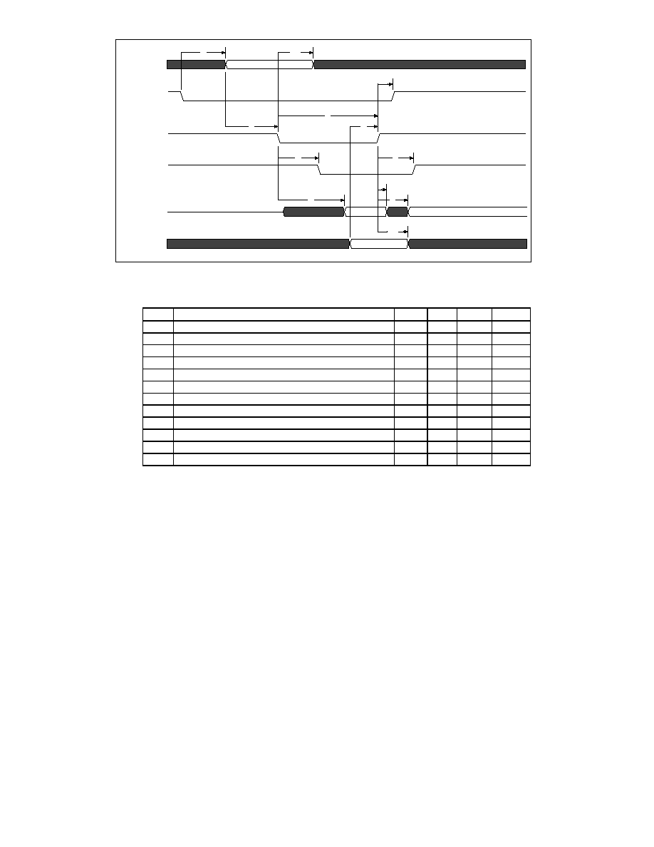
316
t1
t12
t11
t2
t3
t9
t4
t5
t6
t7
t8
t10
SA[15:0]
AEN
nIOR, nIOW
nNOWS
Read Data
Write Data
FIGURE 38 - ZERO WAIT-STATE (NOWS) TIMING
Table 102 - Zero Wait-State Timing Parameters
Parameter
min
typ
max
units
t1
AEN valid before nIOR, nIOW asserted
10
ns
t2
SA[15:0] valid before nIOR asserted
10
ns
t3
nIOR, nIOW pulse width
80
ns
t4
nIOR, nIOW asserted to nNOWS asserted
50
ns
t5
nIOR, nIOW negated to nNOWS floated
35
ns
t6
nIOR asserted to read data valid
50
ns
t7
nIOR negated to read data invalid (hold time)
0
ns
t8
nIOR negated to data bus floated
24
ns
t9
Write data valid before nIOW deasserted
45
ns
t10
nIOW negated to write data invalid (hold time)
0
ns
t11
nIOR, nIOW negated to AEN invalid
10
ns
t12
nIOR, nIOW negated to SA[15:0] invalid
10
ns
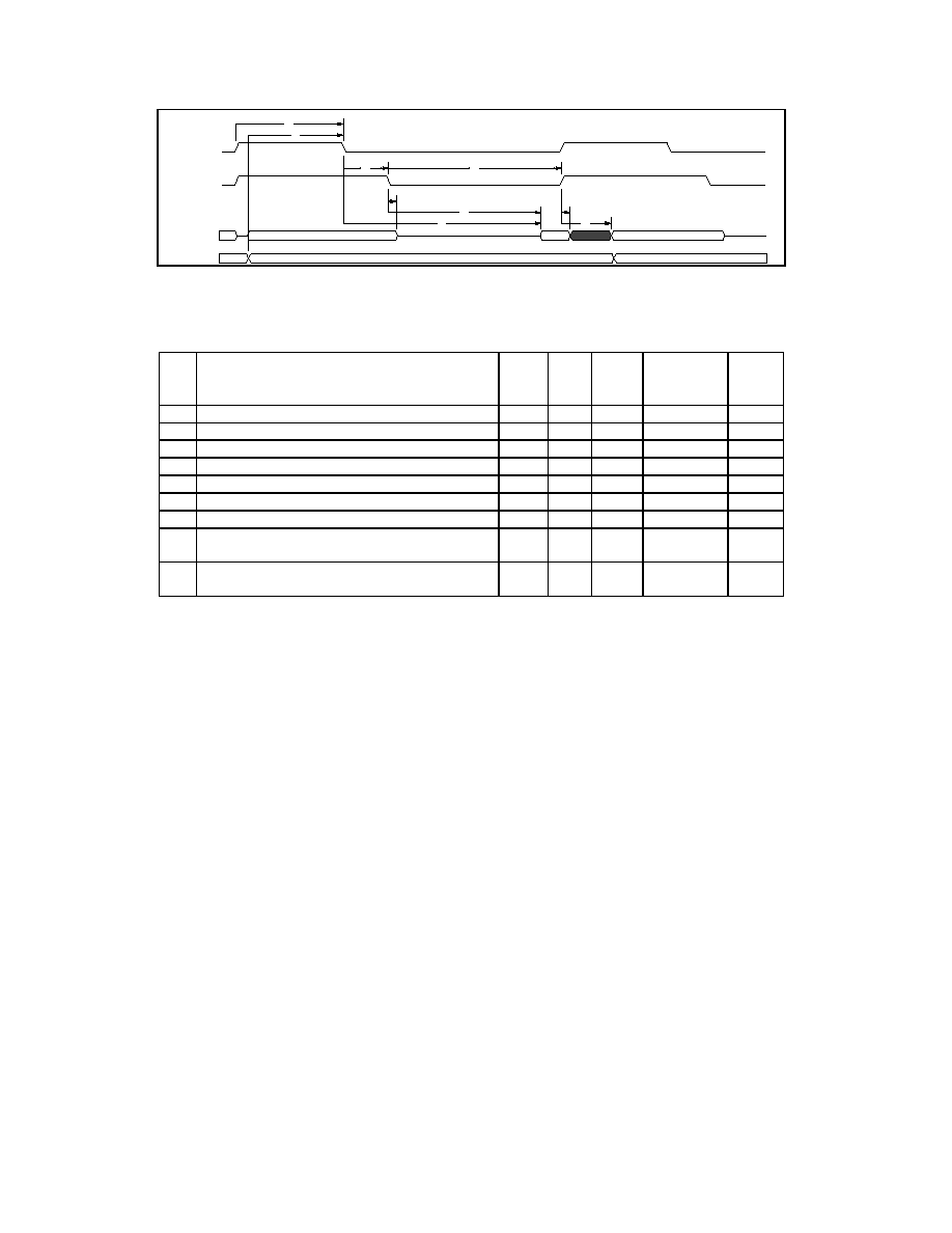
317
FIGURE 39 - 8051 FLASH PROGRAM FETCH TIMING
Table 103 - 8051 Flash Program Fetch Timing Parameters
Parameter
min
typ
max
Oscillato
r
Equation
units
t1
FALE Pulse Width.
127
2T-40
ns
t2
Address Valid to FALE low.
43
T-40
ns
t3
nFRD low to Address float.
10
10
ns
t4
FALE low to Valid Instruction in.
234
4T-100
ns
t5
FALE low to nFRD low.
53
T-30
ns
t6
nFRD Pulse Width.
205
3T-45
ns
t7
nFRD low to Valid Instruction in.
145
3T-105
ns
t8
Valid Instruction hold time following nFRD
low-to-high transition.
0
0
ns
t9
Instruction float following nFRD low-to-high
transition.
59
T-25
ns
Min and Max delays shown for an 8051 clock of 12MHz, to calculate timing delays for other
clock frequencies use the Oscillator Equations, where T=1/Fclk.
t2
t1
t5
t6
t3
t4
t7
t8
t9
INS
FA[7:0]
FA[7:0]
FA[17:8]
FA[17:8]
FALE
FRD
FAD[7:0]
FA[17:8]

318
FIGURE 40 - 8051 FLASH READ TIMING
Table 104 - Flash Read Timing Parameters
Parameter
min
typ
max
Oscillator
Equation
units
t1
Address Valid to FALE low.
43
T-40
ns
t2
Address Hold Following FALE low..
53
T-30
ns
t3
FALE low to nFRD low.
200
300
3T-50 / 3T+50
ns
t4
nFRD Pulse Width.
400
6T-100
ns
t5
nFRD high to FALE high.
43
123
T-40 / T+40
ns
t6
nFRD low to Valid Data In
252
5T-165
ns
t7
Data Hold following nFRD.
0
0
ns
t8
Data Float following nFRD.
107
2T-60
ns
Min and Max delays shown for an 8051 clock of 12MHz, to calculate timing delays for other clock
frequencies use the Oscillator Equations, where T=1/Fclk.
t1
t5
t3
t4
t2
t6
t7
t8
DATA IN
FA[17:8]
FA[7:0]
FA[17:8]
FA[7:0
FALE
nFRD
FAD[7:0]
FA[17:8]
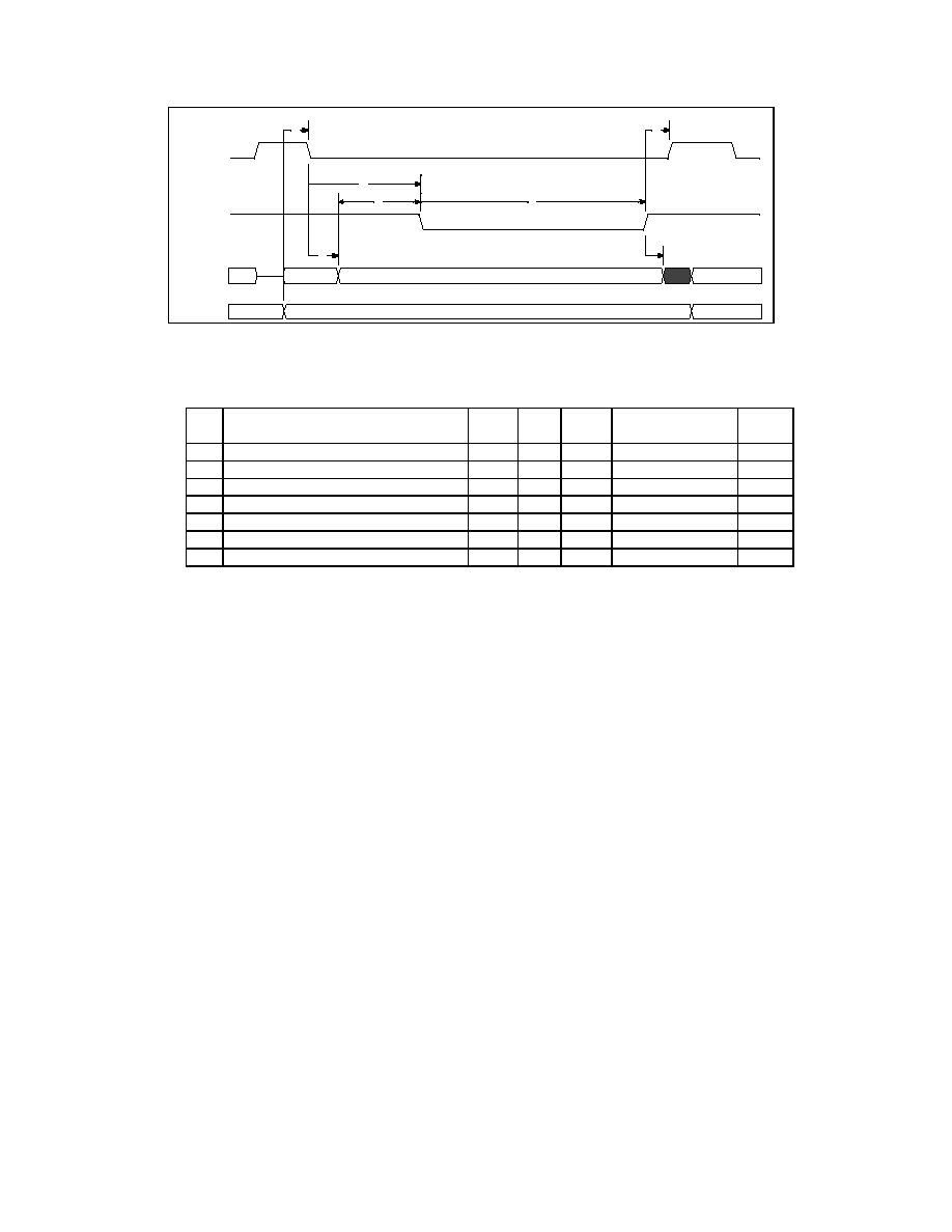
319
t6
t1
t5
t3
t4
t2
t7
FA[17:8]
DATA OUT
FA[17:8]
FA[7:0]
FA[7:0]
FALE
nFWR
FAD[7:0]
FA[17:8]
FIGURE 41 - 8051 FLASH WRITE TIMING
Table 105 - Flash Write Timing Parameters
Parameter
min
typ
max
Oscillator
Equation
units
t1
Address Valid to FALE low.
43
T-40
ns
t2
Address Hold Following FALE low.
53
T-30
ns
t3
FALE low to nFWR low.
200
300
3T-50 / 3T+50
ns
t4
nFWR Pulse Width.
400
6T-100
ns
t5
nFWR high to FALE high.
43
123
T-40 / T+40
ns
t6
Data Valid to nFWR falling edge
33
T-50
ns
t7
Data Hold following nFWR.
33
T-50
ns
Min and Max delays shown for an 8051 clock of 12MHz, to calculate timing delays for other
clock frequencies use the Oscillator Equations, where T=1/Fclk.

320
A
A1
A2
D
D1
E
E1
H
L
MIN
0.05
3.17
30.35
27.90
30.35
27.90
0.09
0.35
NOM
30.60
28.00
30.60
28.00
0.50
MAX
4.07
0.5
3.67
30.85
28.10
30.85
28.10
0.230
0.65
NOM
1.30
0.50BSC
0.20 or 0.15
0.30 or 0.20
MIN
0
0.10
MAX
7
0.30
L1
e
0
W
R1
R2
Notes:
1)
Coplanarity is 0.080 mm maximum
2)
Tolerance on the position of the leads is 0.080 mm maximum
3)
Package body dimensions D1 and E1 do not include the mold protrusion.
Maximum mold protrusion is 0.25 mm
4)
Dimensions for foot length L when measured at the centerline of the leads
are given at the table. Dimension for foot length L when measured at the
gauge plane 0.25 mm above the seating plane, is 0.6 mm
5)
Details of pin 1 identifier are optional but must be located within the zone indicated
6)
Controlling dimension: millimeter
FIGURE 42 - 208 PIN QFP PACKAGE OUTLINE
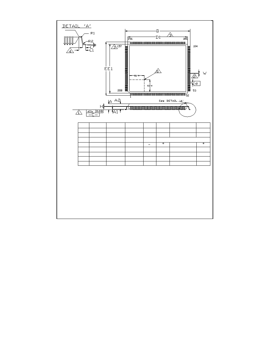
321
A
A 1
A 2
D
D 1
E
E 1
H
M I N
0.05
1.35
29.90
27.90
29.90
27.90
0.09
N O M
30.00
28.00
30.00
28.00
M A X
1.6
0.15
1.45
30.10
28.10
30.10
28.10
0.230
N O M
0.60
1.00
0 . 5 0 B S C
M I N
0.45
0
0.17
0.08
0.08
M A X
0.75
7
0.27
0.20
0.08
L
L1
e
0
W
R 1
R 2
c c c
Notes:
1)
Coplanarity is 0.080 mm or 3.2 mils maximum
2)
Tolerance on the position of the leads is 0.080 mm maximum
3)
Package body dimensions D1 and E1 do not include the mold protrusion.
Maximum mold protrusion is 0.25 mm
5)
Details of pin 1 identifier are optional but must be located within the zone
indicated
6)
Controlling dimension: millimeter
4)
Dimensions for foot length L measured at the gauge plane 0.25 mm above
the seating plane
FIGURE 43 - 208 PIN TQFP PACKAGE OUTLINE

©1996 STANDARD MICROSYSTEMS
CORP.
Circuit diagrams utilizing SMC products are included as a means of illustrating
typical applications; consequently complete information sufficient for construction
purposes is not necessarily given. The information has been carefully checked and
is believed to be entirely reliable. However, no responsibility is assumed for
inaccuracies. Furthermore, such information does not convey to the purchaser of
the semiconductor devices described any licenses under the patent rights of SMC or
others. SMC reserves the right to make changes at any time in order to improve
design and supply the best product possible. SMC products are not designed,
intended, authorized or warranted for use in any life support or other application
where product failure could cause or contribute to personal injury or severe property
damage. Any and all such uses without prior written approval of an Officer of SMC
and further testing and/or modification will be fully at the risk of the customer.
FDC37C957FR Rev. 7/29/96