 | –≠–ª–µ–∫—Ç—Ä–æ–Ω–Ω—ã–π –∫–æ–º–ø–æ–Ω–µ–Ω—Ç: LAN83C175 | –°–∫–∞—á–∞—Ç—å:  PDF PDF  ZIP ZIP |

LAN83C175
ADVANCE INFORMATION
LAN83C175 - EPIC/C
Ethernet CARDBUS Integrated Controller With
Modem Support
FEATURES
∑
IEEE 802.3 Compliant 10/100 Mb/s
Ethernet Controller
∑
Fully Compliant Glueless Integrated
CardBus Interface
∑
Secondary 8 Bit interface to Support Multi-
function CardBus Adpaters Including LAN /
Rockwell or Lucent Modem Combinations
∑
Supports 3.3V or 5V Modem and Physical
Layer Interface
∑
10Base-T Physical Layer Digital Support
-
Smart Squelch Digital Noise Filter and
Receive and Collision Input to Reject
Both Analog and Digital Noise on
Twisted Pair Receive Inputs
-
10Mbps Manchester Encoding /
Decoding with Receive Clock
Recovery
-
Automatic Polarity Detection
-
Full Duplex Support
∑
Scatter/Gather DMA Capability
∑
Supports Chaining of Transmit Packets
∑
Optional Early Transmit and Early Receive
∑
Optional Receive Lookahead Buffering
Mode
∑
4.5Kbyte On-Chip Receive Buffer and
1.5Kbyte On-Chip Transmit Buffer
Eliminate Bus Latency Issues
∑
Automatic Rejection of Runt Packets
∑
Automatic Retransmission of Collision
Frames from Internal Buffer
∑
Automatic Padding of Short Frames
∑
Big or Little Endian Byte Ordering
∑
Capable of Supporting 64Kbyte Expansion
Boot ROM
∑
IEEE Standard MII Interface to Physical
Layer
∑
Interface to LAN83C694 Shares MII Pins
∑
Serial MII Management Interface
∑
Interface to an 8 Bit Parallel EEPROM for
Storage and Retrieval of LAN Address and
Configuration Information
∑
On-Chip Clock Multiplier
∑
Low Power Sleep Mode and Extended
Power Management Features
∑
Internal and External Loopback Diagnostic
Functions
∑
Simple I/O Pin Mapping Scheme to
Facilitate In-Circuit Test
∑
Single 3.3V Supply
∑
208 Pin TQFP Package

2
TABLE OF CONTENTS
FEATURES ........................................................................................................................................1
GENERAL DESCRIPTION .................................................................................................................3
PIN CONFIGURATION.......................................................................................................................5
DESCRIPTION OF PIN FUNCTIONS .................................................................................................6
FUNCTIONAL DESCRIPTION............................................................................................................9
DMA OPERATION............................................................................................................................11
TRANSMIT DMA ..............................................................................................................................11
RECEIVE DMA .................................................................................................................................17
TRANSMIT/RECEIVE ARBITRATION FOR
C
ARD
B
US
BUS...............................................................25
BIG/LITTLE ENDIAN SUPPORT.......................................................................................................25
MAC O
PERATION
................................................................................................................................28
MAC R
ECEIVER
..................................................................................................................................28
MAC TRANSMITTER........................................................................................................................30
MII MANAGEMENT INTERFACE......................................................................................................32
EEPROM INTERFACE .....................................................................................................................32
POWER DOWN MODE ....................................................................................................................34
JUMPER OPTIONS ..........................................................................................................................34
SOFT RESET ...................................................................................................................................34
CONFIGURATION ...........................................................................................................................35
M
APPING OF
ROM
AND
C
ONTROL
F
UNCTIONS
.........................................................................................35
R
EGISTER
M
AP
/C
ONTROL
R
EGISTER
D
ECODE
..........................................................................................37
REGISTER DESCRIPTIONS/CONTROL REGISTERS .....................................................................38
MODEM AND EXTERNAL FLASH RAM INTERFACE AND CONTROL ...........................................64
MODEM REGISTERS MAP .............................................................................................................64
M
ODEM
R
EGISTERS
B
ITS
D
ESCRIPTION
...................................................................................................65
P
HYSICAL
C
ONNECTION
........................................................................................................................68
M
ODEM AND
RAM A
CCESS
T
IMING
.........................................................................................................68
OPERATIONAL DESCRIPTION .......................................................................................................69
M
AXIMUM
G
UARANTEED
R
ATINGS
...........................................................................................................69
DC E
LECTRICAL
C
HARACTERISTICS
........................................................................................................69
TIMING DIAGRAMS ........................................................................................................................71
80 Arkay Drive
Hauppauge, NY. 11788
(516) 435-6000
FAX (516) 273-3123

3
GENERAL DESCRIPTION
The LAN83C175 EPIC/C is a high-performance
Low CPU Utilization Ethernet network controller
designed to interface directly to the CardBus
Local Bus on one side and to the 802.3 standard
Media Independent Interface (MII) on the other
side. The network interface can also be
configured to communicate directly with the
LAN83C694 10BASE-T transceiver.
The LAN83C175 implements 802.3 Media
Access Control functions. It is capable of
running at Ethernet rates of both 100Mbps and
10Mbps. An MII compliant serial management
interface is provided to control external media
dependent transceivers. The LAN83C175 is a
two channel bus master (one for transmit, one
for receive) capable of transferring data at the
maximum CardBus transfer rate of 132Mbps.
The LAN83C175 has several features designed
to maximize throughput and minimize CPU
utilization, including the optional Receive
Lookahead Buffering Mode, which eliminates the
need to re-copy the data from one host memory
location to another.
The LAN83C175 also includes a secondary
general purpose 8-bit interface with appropriate
registers, address lines and control lines. This
secondary interface provides all of the signals
required to implement a secondary function on
a CardBus adpater. An example of such a
secondary function is a 33.6Kbps or higher
speed modem design based on a Rockewell or
Lucent modem chip set.
4
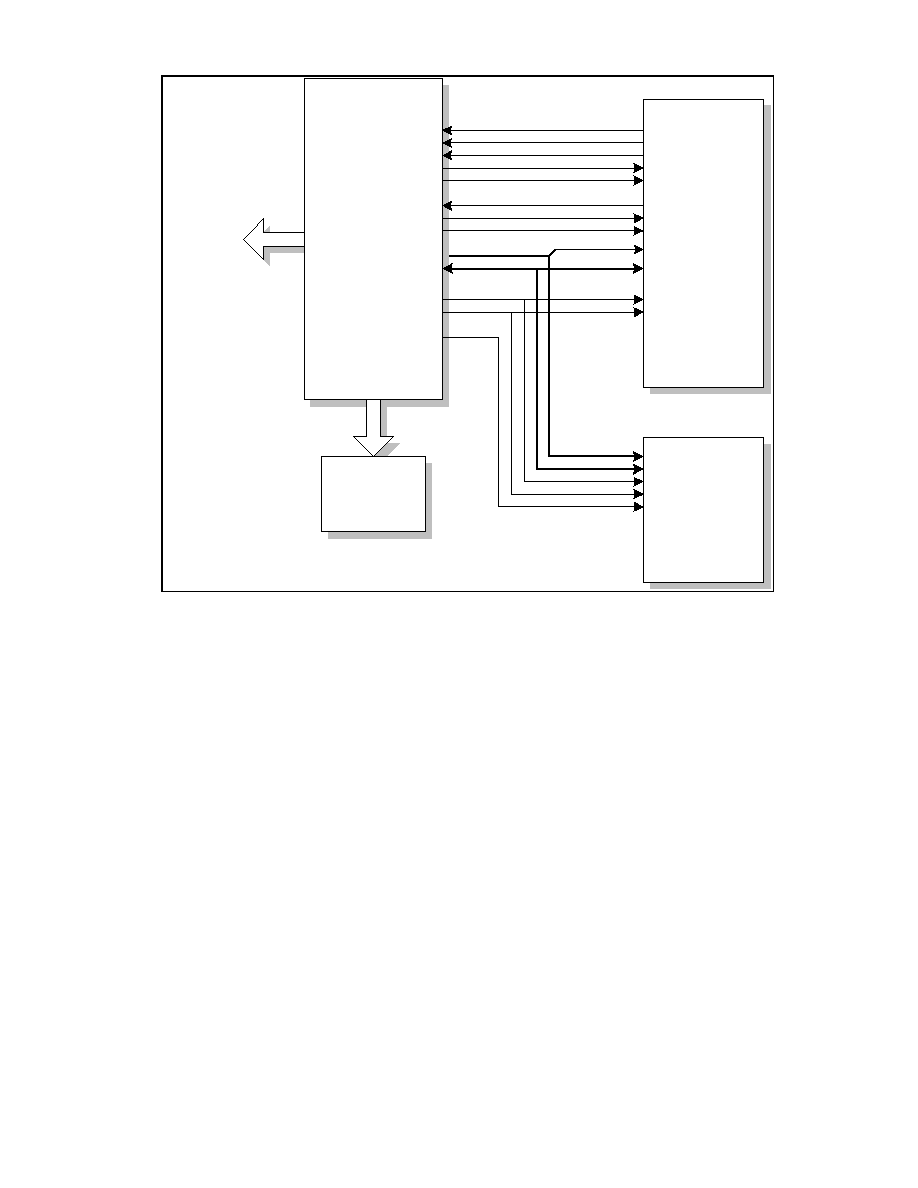
FIGURE 1 - LAN83C175 SYSTEM DIAGRAM
MA(15:0)
WR_N
RAMCS_N
MD(7:0)
MA(x:0)
RD_N
MCS_N
MRESET_N
MPWRDWN
HINT
IREQM
RDYM
RDYM
RINGIN
RINGOUT
RINGIN
RINGOUT
PWRDWN
~RESET
~HCS
HA(x:0)
~HWT
~HRD
AUDIO
AUDIOIN
ADDR(15:0)
DATA(7:0)
RAMWE_N
RAMOE_N
RAMCS_N
HD(7:0)
Epic/C
Modem
RAM
Cardbus
Interface
Cardbus
Physical Layer
Interface
PHY

5
PIN CONFIGURATION
LAN83C175
208 Pin TQFP
1
2
3
4
5
6
7
8
9
10
11
12
13
14
15
16
17
18
19
20
21
22
23
24
25
26
27
28
29
30
31
32
33
34
35
36
37
38
39
40
41
42
43
44
45
46
47
48
49
50
51
52
VDD
PHY
GND
N/C
COL
TX_CLK
FETPWR_PHY
GND
X20
VDD
3.3
VDD
3.3
BIAS
ZENER
GND
CLK25IN
nPHY_PWRDWN
GND
694nEN
VDD
PHY
694nLNK
TEST
GPIO1
GPIO2
N/C
VDD
3.3
GND
GND
nCINT
nRST
GND
CBCLK
VDD
3.3
nCCLKRUN
nCGNT
GND
nCREQ
VDD
3.3
N/C
GND
CAD31
CAD30
VDD
3.3
CAD29
GND
CAD28
CAD27
VDD
3.3
CAD26
CAD25
GND
STATCHG
VDD
3.3
GND
5
3
5
4
5
5
5
6
5
7
5
8
5
9
6
0
6
1
6
2
6
3
6
4
6
5
6
6
6
7
6
8
6
9
7
0
7
1
7
2
7
3
7
4
7
5
7
6
7
7
7
8
7
9
8
0
8
1
8
2
8
3
8
4
8
5
8
6
8
7
8
8
8
9
9
0
9
1
9
2
9
3
9
4
9
5
9
6
9
7
9
8
9
9
1
0
0
1
0
1
1
0
2
1
0
3
1
0
4
V
D
D
3
.
3
G
N
D
N
/
C
A
U
D
I
O
O
U
T
V
D
D
3
.
3
C
A
D
2
4
n
C
B
E
3
G
N
D
C
A
D
2
3
C
A
D
2
2
C
A
D
2
1
V
D
D
3
.
3
C
A
D
2
0
C
A
D
1
9
G
N
D
C
A
D
1
8
C
A
D
1
7
G
N
D
C
A
D
1
6
n
C
B
E
2
V
D
D
3
.
3
n
C
F
R
A
M
E
n
C
I
R
D
Y
G
N
D
N
/
C
n
C
T
R
D
Y
n
C
D
E
V
S
E
L
V
D
D
3
.
3
n
C
S
T
O
P
n
C
B
L
O
C
K
G
N
D
n
C
P
E
R
R
n
C
S
E
R
R
V
D
D
3
.
3
C
P
A
R
n
C
B
E
1
G
N
D
V
D
D
3
.
3
C
A
D
1
5
C
A
D
1
4
G
N
D
C
A
D
1
3
C
A
D
1
2
V
D
D
3
.
3
C
A
D
1
1
N
/
C
G
N
D
C
A
D
1
0
C
A
D
9
C
A
D
8
V
D
D
3
.
3
G
N
D
156
155
154
153
152
151
150
149
148
147
146
145
144
143
142
141
140
139
138
137
136
135
134
133
132
131
130
129
128
127
126
125
124
123
122
121
120
119
118
117
116
115
114
113
112
111
110
109
108
107
106
105
VDD
MOD
GND
N/C
MD1/JMP1
MD0/JMP0
MA15
MA14
N/C
MA13
MA12
VDD
3.3
MA11
GND
MA10
VDD
MOD
MA9
VDD
MOD
MA8
GND
MA7
MA6
GND
MA5
MA4
GND
MA3
MA2
MA1
MA0
N/C
GND
VDD
3.3
GND
N/C
VDD
3.3
CAD0
CAD1
GND
CAD2
CAD3
GND
VDD
3.3
CAD4
CAD5
GND
CAD6
N/C
VDD
3.3
CAD7
nCBE0
GND
VDD
3.3
2
0
8
2
0
7
2
0
6
2
0
5
2
0
4
2
0
3
2
0
2
2
0
1
2
0
0
1
9
9
1
9
8
1
9
7
1
9
6
1
9
5
1
9
4
1
9
3
1
9
2
1
9
1
1
9
0
1
8
9
1
8
8
1
8
7
1
8
6
1
8
5
1
8
4
1
8
3
1
8
2
1
8
1
1
8
0
1
7
9
1
7
8
1
7
7
1
7
6
1
7
5
1
7
4
1
7
3
1
7
2
1
7
1
1
7
0
1
6
9
1
6
8
1
6
7
1
6
6
1
6
5
1
6
4
1
6
3
1
6
2
1
6
1
1
6
0
1
5
9
1
5
8
1
5
7
V
D
D
P
H
Y
G
N
D
R
X
_
C
L
K
V
D
D
3
.
3
R
X
_
D
V
R
X
_
E
R
M
D
A
T
A
G
N
D
M
C
L
K
P
H
Y
R
S
T
T
X
_
E
N
G
N
D
T
X
D
3
T
X
D
2
G
N
D
T
X
D
1
T
X
D
0
V
D
D
P
H
Y
G
N
D
R
X
D
3
R
X
D
2
V
D
D
P
H
Y
R
X
D
1
R
X
D
0
C
R
S
N
/
C
N
/
C
F
E
T
P
W
R
M
P
O
W
E
R
D
W
N
M
n
R
E
S
E
T
M
R
I
N
G
O
U
T
n
R
O
M
C
S
n
C
S
M
N
/
C
V
D
D
3
.
3
n
M
E
M
R
D
n
M
E
M
W
R
V
D
D
M
O
D
R
I
N
G
I
N
A
U
D
I
O
I
N
I
R
E
Q
M
G
N
D
R
D
Y
M
M
D
7
M
D
6
G
N
D
M
D
5
M
D
4
M
D
3
M
D
2
/
J
M
P
2
G
N
D
V
D
D
M
O
D