 | –≠–ª–µ–∫—Ç—Ä–æ–Ω–Ω—ã–π –∫–æ–º–ø–æ–Ω–µ–Ω—Ç: SSD1770Z | –°–∫–∞—á–∞—Ç—å:  PDF PDF  ZIP ZIP |

v
TABLE OF CONTENTS
1
GENERAL DESCRIPTION .........................................................................................................................................1
2
FEATURES ....................................................................................................................................................................2
3
ORDERING INFORMATION.....................................................................................................................................2
4
BLOCK DIAGRAM ......................................................................................................................................................3
5
DIE PAD FLOOR PLAN ..............................................................................................................................................4
6
PIN DESCRIPTION....................................................................................................................................................12
7
FUNCTIONAL BLOCK DESCRIPTIONS ..............................................................................................................15
8
COMMAND TABLE...................................................................................................................................................22
9
COMMAND DESCRIPTIONS ..................................................................................................................................30
10
MAXIMUM RATINGS...............................................................................................................................................51
11
DC CHARACTERISTICS..........................................................................................................................................52
12
AC CHARACTERISTICS..........................................................................................................................................53
13
APPLICATION EXAMPLES ....................................................................................................................................57
14
SSD1770Z DIE TRAY DIMENSIONS ......................................................................................................................60

vi
TABLE OF TABLES
Table 1 ≠ Ordering Information...................................................................................................................................2
Table 2 ≠ SSD1770 Series Bump Die Pad Coordinates (Bump center) ....................................................................5
Table 3 ≠ V
OUT
> V
L5
> V
L4
> V
L3
> V
L2
> V
SS
Relationship........................................................................................14
Table 4 ≠ Data bus selection modes ........................................................................................................................16
Table 5 ≠ COMMAND TABLE (D/ C = 0, R/
W
( WR ) = 0, E=1( RD = 1) unless specific setting is stated) .............22
Table 6 - Read Command Table ..............................................................................................................................28
Table 7 - RAM arrangements of 8-levels gray scale mode ......................................................................................30
Table 8 - RAM arrangements of 16-levels gray scale mode ....................................................................................31
Table 9 - RGB Arrangement modes .........................................................................................................................34
Table 10 - Gray scale selection mode ......................................................................................................................34
Table 11 - Area scrolling selection modes................................................................................................................36
Table 12 - Maximum Ratings (Voltage Referenced to V
SS
)......................................................................................51
Table 13 - DC Characteristics (Unless otherwise specified, Voltage Referenced to V
SS
, V
DD
= 2.4 to 3.6V, T
A
= -40
to 85
∞
∞
∞
∞C) .............................................................................................................................................................52
Table 14 - AC Characteristics (Unless otherwise specified, Voltage Referenced to V
SS
, V
DD
= 2.7V, T
A
= 25
o
C) ..53
Table 15 ≠ Parallel Timing Characteristics (T
A
= -40 to 85
∞
∞
∞
∞C, V
DD
= 2.4V to 3.6V) .................................................54
Table 16 ≠ Parallel Timing Characteristics (T
A
= -40 to 85
∞
∞
∞
∞C, V
DD
= 2.4V to 3.6V) .................................................55
Table 17 - Serial Timing Characteristics (T
A
= -40 to 85
∞
∞
∞
∞C, V
DD
= 2.4V to 3.6V) .....................................................56
TABLE OF FIGURES
Figure 1 ≠ SSD1770 Block Diagram...........................................................................................................................3
Figure 2 ≠ SSD1770 Die Pad Floor Plan....................................................................................................................4
Figure 3 ≠ Display Data ............................................................................................................................................15
Figure 4 ≠ Display Data RAM Map ...........................................................................................................................19
Figure 5 ≠ SSD1770 Hardware Configurations ........................................................................................................20
Figure 6 ≠ Oscillator structural block diagram ..........................................................................................................21
Figure 7 - column and page scan direction of 8-level gray scale mode ...................................................................32
Figure 8 - column and page scan direction of 16-level gray scale mode .................................................................33
Figure 9 ≠ Example of Normal or Reverse page/column/ scan directions ...............................................................33
Figure 10 - Examples: 8 gray-scale display arrangement ........................................................................................34
Figure 11 - Area scrolling selection modes ..............................................................................................................36
Figure 12 - GDDRAM updates for area scrolling......................................................................................................37
Figure 13 ≠ Example of Specified Center Scroll Mode.............................................................................................38
Figure 14 - Contrast Control Flow Set Segment Re-map.........................................................................................39
Figure 15 - Contrast Control Voltage Range Curve (V
DD
=2.7V; V
CI
=3V; Booster level = 6X; TC = -0.25%/
o
C) ....40
Figure 16 - Partial display mode...............................................................................................................................41
Figure 17 ≠ OTP programming circuitry ...................................................................................................................47
Figure 18 ≠ Flow chart of OTP programming Procedure .........................................................................................48
Figure 19 ≠ Parallel 6800-series Interface Timing Characteristics (PS0 = H, PS1 = H) ..........................................54
Figure 20 ≠ Parallel 8080-series Interface Timing Characteristics (PS0 = H, PS1 = L)...........................................55
Figure 21 - Serial Timing Characteristics (PS0 = L, PS1 =L) ...................................................................................56
Figure 22 - Application Example I (4-wires SPI mode).............................................................................................57
Figure 23 - Application Example II (6800 PPI mode) ...............................................................................................58
Figure 24 ≠ Applications notes for V
DD
/V
DDIO
connection .........................................................................................59

SOLOMON SYSTECH
SEMICONDUCTOR TECHNICAL DATA
This document contains information on a new product under definition stage. Solomon Systech Limited reserves
the right to change or discontinue this product without notice.
http://www.solomon-systech.com
SSD1770
Rev 1.00 P 1/61
Sep 2003
Copyright
2003 Solomon Systech Limited
SSD1770
Advance Information
LCD Segment / Common COLOR Driver with Controller
CMOS
1 General
Description
SSD1770 is a single-chip CMOS color STN LCD driver with controller for dot-matrix graphic liquid
crystal display system. SSD1770 consists of 393 high voltage driving output pins for driving maximum 104
RGB Segments, 80 Commons and 1 icon-driving Common.
SSD1770 consists of 312 (104 RGB) x 81 x 4 bits Graphic Display Data RAM (GDDRAM).
Data/Commands are sent from common MCU through 8-bit 6800-series / 8080-series compatible Parallel
Interface or 3-wires / 4-wires Serial Peripheral Interface by pins selection.
SSD1770 embeds DC-DC Converter, On-Chip Oscillator and Bias Divider so as to reduce the number of
external components. With the advanced design, low power consumption, stable LCD operating voltage
and flexible die package layout, SSD1770 is suitable for any portable battery-driven applications requiring
long operation period with compact size.
Solomon Systech
Sep 2003
P 2/61
Rev 1.00
SSD1770
2 FEATURES
∑ Power Supply: V
DD
= 2.4 V ≠ 3.6V
V
DDIO
= 2.4 V ≠ 3.6V
V
CI
= 2.4 V ≠ 3.6V
∑ LCD Driving Output Voltage: 12.5V
∑ Low Current Sleep Mode
∑ Maximum display size: 104 RGB columns by 80 rows with one Icon line
∑ Color display support: 256 colors or 4096 colors graphical display
∑ 256-colors Position Control and simultaneous RGB display control
∑ 8-bit 6800-series / 8080-series Parallel Interface, 3-wires / 4-wires Serial Peripheral Interface
∑ On-Chip 312 (104 RGB) X (81) x 4 = 101088 bits Graphic Display Data RAM
∑ Programmable partial display function
∑ Column Re-mapping and RAM Page scan direction control
∑ Software selection on Center Screen Scrolling, Top Screen Scrolling, Bottom Screen Scrolling
and Whole Screen Scrolling
∑ On-Chip Voltage Generator or External LCD Driving Power Supply Selectable
∑ 3X/ 4X / 5X / 6X On-Chip DC-DC Converter with internal flying capacitor
∑ 64 Levels Internal Contrast Control
∑ Programmable LCD Driving Voltage Temperature Compensation Coefficients
∑ On-Chip Bias Divider with internal flying capacitor (expect V
OUT
)
∑ Programmable drive duty ratio: 1 /8 to 1 /81
∑ On-Chip Oscillator
∑ 2-D Graphic Acceleration Engine
∑ Non-Volatile Memory (OTP) for calibration
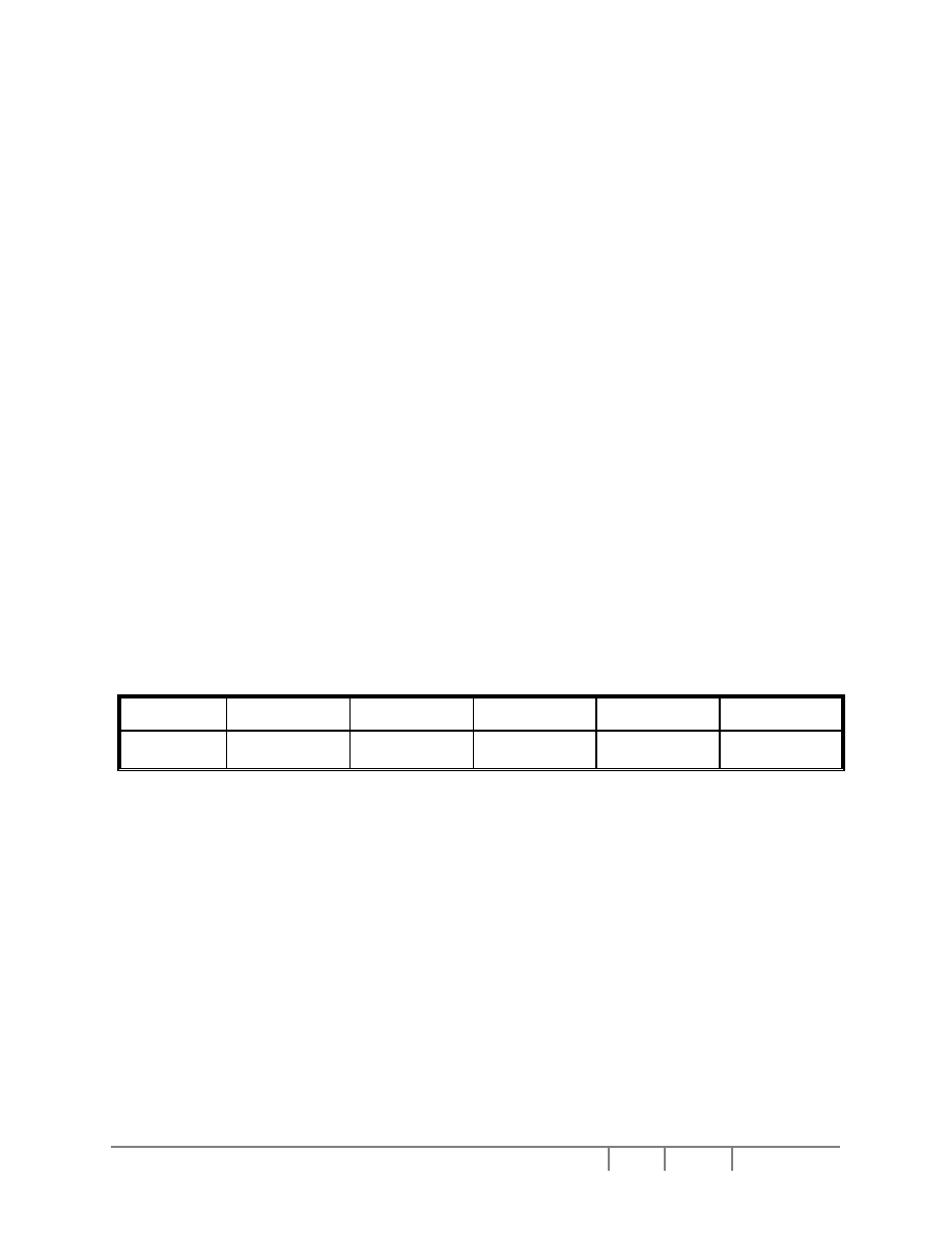
3 ORDERING INFORMATION
Ordering Part
Number
SEG
COM
Display Colors
Package Form
Reference
SSD1770Z 104
81
4096 or
256 colors
Gold Bump Die
Figure 2 on
page 4
Table 1 ≠ Ordering Information

SSD1770
Rev 1.00 P 3/61
Sep 2003
Solomon Systech
4 BLOCK
DIAGRAM
Figure 1 ≠ SSD1770 Block Diagram
COL0 ~ COL311
ROW0 ~ ROW79 ICON
Display Data L
GDDRAM 312 (104RGB)
X 81 X 4 bits
Display
Timing
Generator
Oscillator
Command Decoder
Microprocessor Interface Logic
M
CL
V
CI
104 RGB
Segment
Driver Circuits
81 Common
Driver
Circuits
Page
Address
Control
Circuit
MPU System
Control Circuit
LCD Driving
Voltage
Generator
3X/4X/5X/6X
DC/DC
Converter,
Voltage
Regulator,
Contrast
Control, Bias
Divider,
Temperature
Compensation
Status
Register
V
SS
D0 - D7
E (RD )
R/W
(
WR
)
PS0 PS1
D/C
CS
RES
CV
SS
RV
SS
SYN
BUSY
V
L5
V
OUT
V
L4
V
SS
V
L2
V
L3
2-D Graphic
Acceleration
Engine
V
DD
Column
Address
Control
Circuit
TEST17
TEST0
80
/
68
MUX
V
CIX2
VH
REF
V
L
REF
V
DDIO

Solomon Systech
Sep 2003
P 4/61
Rev 1.00
SSD1770
25 25
25
25
25
25
100
100
5 DIE PAD FLOOR PLAN
Figure 2 ≠ SSD1770 Die Pad Floor Plan
PIN 1
PIN 229
PIN 230
0
,
0
Y
X
Die size: 17.74 mm x 1.88 mm
Die Thickness: 457 ± 25µm
Bump Height: typical 15µm
Bump co-planarity <3µm (within die)
Note:
1. Diagram showing the die face up.
2. Coordinates are reference to center of the chip.
3. Unit of coordinates and Size of all alignment
marks are in um.
4. All alignment keys do not contain gold bump.
18
100
75
100
25 25
25
25
50
100
100
Ce
nt
re
:
-8393.
7,
-602.
825
Ce
nt
re
:
8393.
7,
358.
375
Ce
nt
re
:
8393.
7,
-602.
825
Ce
nt
re
:
-8393.
7,
358.
375
PIN 126
PIN 127
PIN 272
PIN 585
PIN 627

SSD1770
Rev 1.00 P 5/61
Sep 2003
Solomon Systech
Table 2 ≠ SSD1770 Series Bump Die Pad Coordinates (Bump center)
Pad #
Signal
X-pos
Y-pos
Pad #
Signal
X-pos
Y-pos
Pad #
Signal X-pos
Y-pos
1 DUMMY
-8706.0 -769.7
51
C
/
D
-4896.0
-769.7
101 V
CI
-1066.6
-769.7
2 DUMMY
-8629.8 -769.7
52 BUSY
-4819.8
-769.7
102 V
CI
-990.4
-769.7
3 DUMMY
-8553.6 -769.7
53 BUSY
-4743.6
-769.7
103 V
CI
-914.2
-769.7
4 DUMMY
-8477.4 -769.7
54 V
SS
-4667.4
-769.7
104
V
CI
-838.0
-769.7
5 DUMMY
-8401.2 -769.7
55
80
/
68
MUX
-4591.2
-769.7
105 V
CI
-761.8
-769.7
6 DUMMY
-8325.0 -769.7
56 V
DD
-4515.0
-769.7
106
V
CI
-685.6
-769.7
7 TEST0
-8248.8 -769.7
57 TEST1
-4438.8
-769.7
107 V
CI
-609.4
-769.7
8 CL
-8172.6 -769.7
58 TEST2
-4362.6
-769.7
108 V
CI
-533.2
-769.7
9 M
-8096.4 -769.7
59 TEST3
-4286.4
-769.7
109 V
CI
-457.0
-769.7
10 SYN
-8020.2 -769.7
60 TEST4
-4210.2
-769.7
110 V
CI
-380.8
-769.7
11 V
DD
-7944.0
-769.7
61 TEST5
-4134.0
-769.7
111
V
CI
-304.6
-769.7
12 PS0
-7867.8 -769.7
62 TEST6
-4057.8
-769.7
112 V
CI
-228.4
-769.7
13 V
SS
-7791.6
-769.7
63 TEST7
-3981.6
-769.7
113
V
CI
-152.2
-769.7
14 PS1
-7715.4 -769.7
64 TEST8
-3905.4
-769.7
114 V
CI
-76.0
-769.7
15 V
SS
-7639.2
-769.7
65 V
DD
-3829.2
-769.7
115
V
CI
0.2
-769.7
16
CS
-7563.0 -769.7
66 V
DD
-3753.0
-769.7
116 V
CI
76.4
-769.7
17
CS
-7486.8 -769.7
67 V
DD
-3676.8
-769.7
117 V
CI
152.6
-769.7
18 V
DD
-7410.6
-769.7
68 V
DD
-3600.6
-769.7
118 V
CI
228.8
-769.7
19
RES
-7334.4 -769.7
69 V
DD
-3524.4
-769.7
119 V
CI
305.0
-769.7
20
C
/
D
-7258.2 -769.7
70 V
DD
-3448.2
-769.7
120 V
CI
381.2
-769.7
21
C
/
D
-7182.0 -769.7
71 V
DD
-3372.0
-769.7
121 V
CI
457.4
-769.7
22
C
/
D
-7105.8 -769.7
72 V
DD
-3295.8
-769.7
122 V
CI
533.6
-769.7
23 V
SS
-7029.6
-769.7
73 V
DD
-3219.6
-769.7
123 V
CI
609.8
-769.7
24
W
/
R
(
WR
) -6953.4 -769.7
74 V
DD
-3143.4
-769.7
124 V
CI
686.0
-769.7
25
W
/
R
(
WR
) -6877.2 -769.7
75 V
DD
-3067.2
-769.7
125 V
CI
762.2
-769.7
26 E(
RD
) -6801.0
-769.7 76 V
DD
-2991.0
-769.7
126 V
CI
838.4
-769.7
27 E(
RD
) -6724.8
-769.7 77 V
DD
-2914.8
-769.7
127 RV
SS
914.6
-769.7
28 V
DD
-6648.6
-769.7
78 V
DD
-2838.6
-769.7
128 RV
SS
990.8
-769.7
29 D7 (SDA) -6572.4 -769.7
79 V
DD
-2762.4
-769.7
129 RV
SS
1067.0
-769.7
30 D7 (SDA) -6496.2 -769.7
80 V
DD
-2686.2
-769.7
130 CV
SS
1143.2
-769.7
31 D0
-6420.0 -769.7
81 V
DD
-2610.0
-769.7
131 CV
SS
1219.4
-769.7
32 D1
-6343.8 -769.7
82 V
DDIO
-2533.8
-769.7
132 CV
SS
1295.6
-769.7
33 D2
-6267.6 -769.7
83 V
DDIO
-2457.6
-769.7
133 CV
SS
1371.8
-769.7
34 D3
-6191.4 -769.7
84 V
CIX2
-2371.7
-769.7
134
CV
SS
1448.0
-769.7
35 D4
-6115.2 -769.7
85 V
CIX2
-2295.5
-769.7
135 CV
SS
1524.2
-769.7
36 D5
-6039.0 -769.7
86 V
CIX2
-2219.3
-769.7
136 CV
SS
1600.4
-769.7
37 D6 (SCK) -5962.8 -769.7
87 V
CIX2
-2143.1
-769.7
137 CV
SS
1676.6
-769.7
38 D6 (SCK) -5886.6 -769.7
88 V
CIX2
-2066.9
-769.7
138 CV
SS
1752.8
-769.7
39 D6 (SCK) -5810.4 -769.7
89 V
CIX2
-1990.7
-769.7
139 CV
SS
1829.0
-769.7
40 D7 (SDA) -5734.2 -769.7
90 V
CIX2
-1914.5
-769.7
140 CV
SS
1905.2
-769.7
41 D7 (SDA) -5658.0 -769.7
91 V
CIX2
-1838.3
-769.7
141 CV
SS
1981.4
-769.7
42 D7 (SDA) -5581.8 -769.7
92 V
CIX2
-1762.1
-769.7
142 CV
SS
2057.6
-769.7
43 D0
-5505.6 -769.7
93 VH
REF
-1685.9
-769.7
143 CV
SS
2133.8
-769.7
44 V
DD
-5429.4
-769.7
94 VL
REF
-1609.7
-769.7
144 CV
SS
2210.0
-769.7
45
CS
-5353.2 -769.7
95 V
CIX2
-1523.8
-769.7
145 CV
SS
2286.2
-769.7
46
CS
-5277.0 -769.7
96 VL
REF
-1447.6
-769.7
146 CV
SS
2362.4
-769.7
47 V
SS
-5200.8
-769.7
97 V
CI
-1371.4
-769.7
147 CV
SS
2438.6
-769.7
48
RES
-5124.6 -769.7
98 V
CI
-1295.2
-769.7
148 CV
SS
2514.8
-769.7
49
C
/
D
-5048.4 -769.7
99 V
CI
-1219.0
-769.7
149 CV
SS
2591.0
-769.7
50
C
/
D
-4972.2 -769.7
100 V
CI
-1142.8
-769.7
150 CV
SS
2667.2
-769.7
Solomon Systech
Sep 2003
P 6/61
Rev 1.00
SSD1770
Pad #
Signal X-pos
Y-pos
Pad #
Signal X-pos
Y-pos
151 CV
SS
2743.4
-769.7 201 V
L5
6563.1
-769.7
152 CV
SS
2819.6
-769.7 202 TEST17
6639.3
-769.7
153 CV
SS
2895.8
-769.7 203 V
CIX2
6715.5
-769.7
154 CV
SS
2972.0
-769.7 204 VH
REF
6791.7
-769.7
155 TEST9
3048.2 -769.7
205 VH
REF
6867.9
-769.7
156 TEST10
3124.4 -769.7
206 V
OUT
6944.1
-769.7
157 TEST11
3200.6 -769.7
207 V
OUT
7020.3
-769.7
158 TEST12
3276.8 -769.7
208 V
OUT
7096.5
-769.7
159 TEST13
3353.0 -769.7
209 V
OUT
7172.7
-769.7
160 TEST14
3429.2 -769.7
210 V
OUT
7248.9
-769.7
161 TEST15
3505.4 -769.7
211 V
OUT
7325.1
-769.7
162 TEST16
3581.6 -769.7
212 V
OUT
7401.3
-769.7
163 V
SS
3657.8
-769.7
213 V
OUT
7477.5
-769.7
164 V
SS
3734.0 -769.7
214 V
OUT
7553.7
-769.7
165 V
SS
3810.2 -769.7
215 V
OUT
7629.9
-769.7
166 V
SS
3886.4 -769.7
216 V
OUT
7706.1
-769.7
167 V
SS
3962.6 -769.7
217 V
OUT
7782.3
-769.7
168 V
SS
4038.8 -769.7
218 V
OUT
7858.5
-769.7
169 V
SS
4115.0 -769.7
219 SYN
7944.4
-769.7
170 V
SS
4191.2 -769.7
220 CL
8020.6
-769.7
171 V
SS
4267.4 -769.7
221 M
8096.8
-769.7
172 V
SS
4343.6 -769.7
222 CL
8173.0
-769.7
173 V
SS
4419.8 -769.7
223 DUMMY
8249.2
-769.7
174 V
SS
4496.0 -769.7
224 DUMMY
8325.4
-769.7
175 V
SS
4572.2 -769.7
225 DUMMY
8401.6
-769.7
176 V
SS
4648.4 -769.7
226 DUMMY
8477.8
-769.7
177 V
SS
4724.6 -769.7
227 DUMMY
8554.0
-769.7
178 V
SS
4800.8 -769.7
228 DUMMY
8630.2
-769.7
179 V
SS
4877.0 -769.7
229 DUMMY
8706.4
-769.7
180 V
SS
4953.2
-769.7
181 V
SS
5029.4 -769.7
182 V
SS
5105.6 -769.7
183 V
SS
5181.8 -769.7
184 V
SS
5258.0 -769.7
185 V
SS
5334.2 -769.7
186 V
SS
5410.4 -769.7
187 V
SS
5486.6 -769.7
188 V
CIX2
5572.5
-769.7
189 V
CIX2
5648.7
-769.7
190 V
L3
5724.9 -769.7
191 V
L3
5801.1 -769.7
192 V
L3
5877.3 -769.7
193 V
L3
5953.5 -769.7
194 V
L2
6029.7
-769.7
195 V
L2
6105.9
-769.7
196 V
L3
6182.1
-769.7
197 V
L3
6258.3
-769.7
198 V
L4
6334.5
-769.7
199 V
L4
6410.7
-769.7
200 V
L5
6486.9
-769.7

SSD1770
Rev 1.00 P 7/61
Sep 2003
Solomon Systech
Pad # Pad Name
Signal
(
80
MUX68/
=V
DD
) ≠ 68mux
Signal
(
80
MUX68/
=
V
SS
)≠
80 mux
X-pos Y-pos
Pad # Pad Name
Signal
Color
X-pos
Y-pos
230 DUMMY
DUMMY
DUMMY
8745.1
754.3
273 COL311
B
6748.7
754.3
231 DUMMY
DUMMY
DUMMY
8701.7
754.3
274 COL310
G
6705.3
754.3
232 ICONS
ICONS
ICONS
8658.3
754.3
275 COL309
SEG103
R
6661.9
754.3
233 ROW0
COM0
COM0
8614.9
754.3
276 COL308
B
6618.5
754.3
234 ROW1
COM1
COM1
8571.5
754.3
277 COL307
G
6575.1
754.3
235 ROW2
COM2
COM2
8528.1
754.3
278 COL306
SEG102
R
6531.7
754.3
236 ROW3
COM3
COM3
8484.7
754.3
279 COL305
B
6488.3
754.3
237 ROW4
COM4
COM4
8441.3
754.3
280 COL304
G
6444.9
754.3
238 ROW5
COM5
COM5
8397.9
754.3
281 COL303
SEG101
R
6401.5
754.3
239 ROW6
COM6
COM6
8354.5
754.3
282 COL302
B
6358.1
754.3
240 ROW7
COM7
COM7
8311.1
754.3
283 COL301
G
6314.7
754.3
241 ROW8
COM8
COM8
8267.7
754.3
284 COL300
SEG100
R
6271.3
754.3
242 ROW9
COM9
COM9
8224.3
754.3
285 COL299
B
6227.9
754.3
243 ROW10
COM10
COM10
8180.9
754.3
286 COL298
G
6184.5
754.3
244 ROW11
COM11
COM11
8137.5
754.3
287 COL297
SEG99
R
6141.1
754.3
245 ROW12
COM12
COM12
8094.1
754.3
288 COL296
B
6097.7
754.3
246 ROW13
COM13
COM13
8050.7
754.3
289 COL295
G
6054.3
754.3
247 ROW14
COM14
COM14
8007.3
754.3
290 COL294
SEG98
R
6010.9
754.3
248 ROW15
COM15
COM15
7963.9
754.3
291 COL293
B
5967.5
754.3
249 ROW16
COM16
COM16
7920.5
754.3
292 COL292
G
5924.1
754.3
250 ROW17
COM17
COM17
7877.1
754.3
293 COL291
SEG97
R
5880.7
754.3
251 ROW18
COM18
COM18
7833.7
754.3
294 COL290
B
5837.3
754.3
252 ROW19
COM19
COM19
7790.3
754.3
295 COL289
G
5793.9
754.3
253 ROW20
COM20
COM20
7746.9
754.3
296 COL288
SEG96
R
5750.5
754.3
254 ROW21
COM21
COM21
7703.5
754.3
297 COL287
B
5707.1
754.3
255 ROW22
COM22
COM22
7660.1
754.3
298 COL286
G
5663.7
754.3
256 ROW23
COM23
COM23
7616.7
754.3
299 COL285
SEG95
R
5620.3
754.3
257 ROW24
COM24
COM24
7573.3
754.3
300 COL284
B
5576.9
754.3
258 ROW25
COM25
COM25
7529.9
754.3
301 COL283
G
5533.5
754.3
259 ROW26
COM26
COM26
7486.5
754.3
302 COL282
SEG94
R
5490.1
754.3
260 ROW27
COM27
COM27
7443.1
754.3
303 COL281
B
5446.7
754.3
261 ROW28
COM28
COM28
7399.7
754.3
304 COL280
G
5403.3
754.3
262 ROW29
COM29
COM29
7356.3
754.3
305 COL279
SEG93
R
5359.9
754.3
263 ROW30
COM30
COM30
7312.9
754.3
306 COL278
B
5316.5
754.3
264 ROW31
COM31
COM31
7269.5
754.3
307 COL277
G
5273.1
754.3
265 ROW32
COM32
COM32
7226.1
754.3
308 COL276
SEG92
R
5229.7
754.3
266 ROW33
COM33
COM33
7182.7
754.3
309 COL275
B
5186.3
754.3
267 ROW34
Non select signal
COM34 7139.3
754.3
310 COL274
G
5142.9
754.3
268 ROW35
Non select signal
COM35 7095.9
754.3
311 COL273
SEG91
R
5099.5
754.3
269 ROW36
Non select signal
COM36 7052.5
754.3
312 COL272
B
5056.1
754.3
270 ROW37
Non select signal
COM37 7009.1
754.3
313 COL271
G
5012.7
754.3
271 ROW38
Non select signal
COM38 6965.7
754.3
314 COL270
SEG90
R
4969.3
754.3
272 ROW39
Non select signal
COM39 6922.3
754.3
315 COL269
B
4925.9
754.3
316 COL268
G
4882.5
754.3
317 COL267
SEG89
R
4839.1
754.3
318 COL266
B
4795.7
754.3
319 COL265
G
4752.3
754.3
320 COL264
SEG88
R
4708.9
754.3

Solomon Systech
Sep 2003
P 8/61
Rev 1.00
SSD1770
Pad #
Pad Name
Signal
Color
X-pos
Y-pos
Pad #
Pad Name
Signal Color
X-pos
Y-pos
321 COL263
B
4665.5
754.3
369 COL215
B
2582.3
754.3
322 COL262
G
4622.1
754.3
370 COL214
G
2538.9
754.3
323 COL261
SEG87
R
4578.7
754.3
371 COL213
SEG71
R
2495.5
754.3
324 COL260
B
4535.3
754.3
372 COL212
B
2452.1
754.3
325 COL259
G
4491.9
754.3
373 COL211
G
2408.7
754.3
326 COL258
SEG86
R 4448.5
754.3
374 COL210
SEG70
R 2365.3
754.3
327 COL257
B
4405.1
754.3
375 COL209
B
2321.9
754.3
328 COL256
G
4361.7
754.3
376 COL208
G
2278.5
754.3
329 COL255
SEG85
R
4318.3
754.3
377 COL207
SEG69
R
2235.1
754.3
330 COL254
B
4274.9
754.3
378 COL206
B
2191.7
754.3
331 COL253
G
4231.5
754.3
379 COL205
G
2148.3
754.3
332 COL252
SEG84
R
4188.1
754.3
380 COL204
SEG68
R
2104.9
754.3
333 COL251
B
4144.7
754.3
381 COL203
B
2061.5
754.3
334 COL250
G
4101.3
754.3
382 COL202
G
2018.1
754.3
335 COL249
SEG83
R
4057.9
754.3
383 COL201
SEG67
R
1974.7
754.3
336 COL248
B
4014.5
754.3
384 COL200
B
1931.3
754.3
337 COL247
G
3971.1
754.3
385 COL199
G
1887.9
754.3
338 COL246
SEG82
R
3927.7
754.3
386 COL198
SEG66
R
1844.5
754.3
339 COL245
B
3884.3
754.3
387 COL197
B
1801.1
754.3
340 COL244
G
3840.9
754.3
388 COL196
G
1757.7
754.3
341 COL243
SEG81
R
3797.5
754.3
389 COL195
SEG65
R
1714.3
754.3
342 COL242
B
3754.1
754.3
390 COL194
B
1670.9
754.3
343 COL241
G
3710.7
754.3
391 COL193
G
1627.5
754.3
344 COL240
SEG80
R
3667.3
754.3
392 COL192
SEG64
R
1584.1
754.3
345 COL239
B
3623.9
754.3
393 COL191
B
1540.7
754.3
346 COL238
G
3580.5
754.3
394 COL190
G
1497.3
754.3
347 COL237
SEG79
R
3537.1
754.3
395 COL189
SEG63
R
1453.9
754.3
348 COL236
B
3493.7
754.3
396 COL188
B
1410.5
754.3
349 COL235
G
3450.3
754.3
397 COL187
G
1367.1
754.3
350 COL234
SEG78
R
3406.9
754.3
398 COL186
SEG62
R
1323.7
754.3
351 COL233
B
3363.5
754.3
399 COL185
B
1280.3
754.3
352 COL232
G
3320.1
754.3
400 COL184
G
1236.9
754.3
353 COL231
SEG77
R
3276.7
754.3
401 COL183
SEG61
R
1193.5
754.3
354 COL230
B
3233.3
754.3
402 COL182
B
1150.1
754.3
355 COL229
G
3189.9
754.3
403 COL181
G
1106.7
754.3
356 COL228
SEG76
R
3146.5
754.3
404 COL180
SEG60
R
1063.3
754.3
357 COL227
B
3103.1
754.3
405 COL179
B
1019.9
754.3
358 COL226
G
3059.7
754.3
406 COL178
G
976.5
754.3
359 COL225
SEG75
R
3016.3
754.3
407 COL177
SEG59
R
933.1
754.3
360 COL224
B
2972.9
754.3
408 COL176
B
889.7
754.3
361 COL223
G
2929.5
754.3
409 COL175
G
846.3
754.3
362 COL222
SEG74
R
2886.1
754.3
410 COL174
SEG58
R
802.9
754.3
363 COL221
B
2842.7
754.3
411 COL173
B
759.5
754.3
364 COL220
G
2799.3
754.3
412 COL172
G
716.1
754.3
365 COL219
SEG73
R
2755.9
754.3
413 COL171
SEG57
R
672.7
754.3
366 COL218
B
2712.5
754.3
414 COL170
B
629.3
754.3
367 COL217
G
2669.1
754.3
415 COL169
G
585.9
754.3
368 COL216
SEG72
R
2625.7
754.3
416 COL168
SEG56
R
542.5
754.3

SSD1770
Rev 1.00 P 9/61
Sep 2003
Solomon Systech
Pad #
Pad Name
Signal
Color
X-pos
Y-pos
Pad #
Pad Name
Signal
Color X-pos
Y-pos
417 COL167
B
499.1
754.3
465 COL119
B
-1584.1
754.3
418 COL166
G
455.7
754.3
466 COL118
G
-1627.5
754.3
419 COL165
SEG55
R
412.3
754.3
467 COL117
SEG39
R
-1670.9
754.3
420 COL164
B
368.9
754.3
468 COL116
B
-1714.3
754.3
421 COL163
G
325.5
754.3
469 COL115
G
-1757.7
754.3
422 COL162
SEG54
R 282.1
754.3
470 COL114
SEG38
R -1801.1
754.3
423 COL161
B
238.7
754.3
471 COL113
B
-1844.5
754.3
424 COL160
G
195.3
754.3
472 COL112
G
-1887.9
754.3
425 COL159
SEG53
R
151.9
754.3
473 COL111
SEG37
R
-1931.3
754.3
426 COL158
B
108.5
754.3
474 COL110
B
-1974.7
754.3
427 COL157
G
65.1
754.3
475 COL109
G
-2018.1
754.3
428 COL156
SEG52
R
21.7
754.3
476 COL108
SEG36
R
-2061.5
754.3
429 COL155
B
-21.7
754.3
477 COL107
B
-2104.9
754.3
430 COL154
G
-65.1
754.3
478 COL106
G
-2148.3
754.3
431 COL153
SEG51
R
-108.5
754.3
479 COL105
SEG35
R
-2191.7
754.3
432 COL152
B
-151.9
754.3
480 COL104
B
-2235.1
754.3
433 COL151
G
-195.3
754.3
481 COL103
G
-2278.5
754.3
434 COL150
SEG50
R
-238.7
754.3
482 COL102
SEG34
R
-2321.9
754.3
435 COL149
B
-282.1
754.3
483 COL101
B
-2365.3
754.3
436 COL148
G
-325.5
754.3
484 COL100
G
-2408.7
754.3
437 COL147
SEG49
R
-368.9
754.3
485 COL99
SEG33
R
-2452.1
754.3
438 COL146
B
-412.3
754.3
486 COL98
B
-2495.5
754.3
439 COL145
G
-455.7
754.3
487 COL97
G
-2538.9
754.3
440 COL144
SEG48
R
-499.1
754.3
488 COL96
SEG32
R
-2582.3
754.3
441 COL143
B
-542.5
754.3
489 COL95
B
-2625.7
754.3
442 COL142
G
-585.9
754.3
490 COL94
G
-2669.1
754.3
443 COL141
SEG47
R
-629.3
754.3
491 COL93
SEG31
R
-2712.5
754.3
444 COL140
B
-672.7
754.3
492 COL92
B
-2755.9
754.3
445 COL139
G
-716.1
754.3
493 COL91
G
-2799.3
754.3
446 COL138
SEG46
R
-759.5
754.3
494 COL90
SEG30
R
-2842.7
754.3
447 COL137
B
-802.9
754.3
495 COL89
B
-2886.1
754.3
448 COL136
G
-846.3
754.3
496 COL88
G
-2929.5
754.3
449 COL135
SEG45
R
-889.7
754.3
497 COL87
SEG29
R
-2972.9
754.3
450 COL134
B
-933.1
754.3
498 COL86
B
-3016.3
754.3
451 COL133
G
-976.5
754.3
499 COL85
G
-3059.7
754.3
452 COL132
SEG44
R
-1019.9
754.3
500 COL84
SEG28
R
-3103.1
754.3
453 COL131
B
-1063.3
754.3
501 COL83
B
-3146.5
754.3
454 COL130
G
-1106.7
754.3
502 COL82
G
-3189.9
754.3
455 COL129
SEG43
R
-1150.1
754.3
503 COL81
SEG27
R
-3233.3
754.3
456 COL128
B
-1193.5
754.3
504 COL80
B
-3276.7
754.3
457 COL127
G
-1236.9
754.3
505 COL79
G
-3320.1
754.3
458 COL126
SEG42
R
-1280.3
754.3
506 COL78
SEG26
R
-3363.5
754.3
459 COL125
B
-1323.7
754.3
507 COL77
B
-3406.9
754.3
460 COL124
G
-1367.1
754.3
508 COL76
G
-3450.3
754.3
461 COL123
SEG41
R
-1410.5
754.3
509 COL75
SEG25
R
-3493.7
754.3
462 COL122
B
-1453.9
754.3
510 COL74
B
-3537.1
754.3
463 COL121
G
-1497.3
754.3
511 COL73
G
-3580.5
754.3
464 COL120
SEG40
R
-1540.7
754.3
512 COL72
SEG24
R
-3623.9
754.3
Solomon Systech
Sep 2003
P 10/61 Rev 1.00
SSD1770
Pad #
Pad Name
Signal
Color
X-pos
Y-pos
Pad #
Pad Name
Signal
Color X-pos
Y-pos
513 COL71
B
-3667.3
754.3
561 COL23
B
-5750.5
754.3
514 COL70
G
-3710.7
754.3
562 COL22
G
-5793.9
754.3
515 COL69
SEG23
R
-3754.1
754.3
563 COL21
SEG7
R
-5837.3
754.3
516 COL68
B
-3797.5
754.3
564 COL20
B
-5880.7
754.3
517 COL67
G
-3840.9
754.3
565 COL19
G
-5924.1
754.3
518 COL66
SEG22
R -3884.3
754.3
566 COL18
SEG6
R -5967.5
754.3
519 COL65
B
-3927.7
754.3
567 COL17
B
-6010.9
754.3
520 COL64
G
-3971.1
754.3
568 COL16
G
-6054.3
754.3
521 COL63
SEG21
R
-4014.5
754.3
569 COL15
SEG5
R
-6097.7
754.3
522 COL62
B
-4057.9
754.3
570 COL14
B
-6141.1
754.3
523 COL61
G
-4101.3
754.3
571 COL13
G
-6184.5
754.3
524 COL60
SEG20
R
-4144.7
754.3
572 COL12
SEG4
R
-6227.9
754.3
525 COL59
B
-4188.1
754.3
573 COL11
B
-6271.3
754.3
526 COL58
G
-4231.5
754.3
574 COL10
G
-6314.7
754.3
527 COL57
SEG19
R
-4274.9
754.3
575 COL9
SEG3
R
-6358.1
754.3
528 COL56
B
-4318.3
754.3
576 COL8
B
-6401.5
754.3
529 COL55
G
-4361.7
754.3
577 COL7
G
-6444.9
754.3
530 COL54
SEG18
R
-4405.1
754.3
578 COL6
SEG2
R
-6488.3
754.3
531 COL53
B
-4448.5
754.3
579 COL5
B
-6531.7
754.3
532 COL52
G
-4491.9
754.3
580 COL4
G
-6575.1
754.3
533 COL51
SEG17
R
-4535.3
754.3
581 COL3
SEG1
R
-6618.5
754.3
534 COL50
B
-4578.7
754.3
582 COL2
B
-6661.9
754.3
535 COL49
G
-4622.1
754.3
583 COL1
G
-6705.3
754.3
536 COL48
SEG16
R
-4665.5
754.3
584 COL0
SEG0
R
-6748.7
754.3
537 COL47
B
-4708.9
754.3
538 COL46
G
-4752.3
754.3
539 COL45
SEG15
R
-4795.7
754.3
540 COL44
B
-4839.1
754.3
541 COL43
G
-4882.5
754.3
542 COL42
SEG14
R
-4925.9
754.3
543 COL41
B
-4969.3
754.3
544 COL40
G
-5012.7
754.3
545 COL39
SEG13
R
-5056.1
754.3
546 COL38
B
-5099.5
754.3
547 COL37
G
-5142.9
754.3
548 COL36
SEG12
R
-5186.3
754.3
549 COL35
B
-5229.7
754.3
550 COL34
G
-5273.1
754.3
551 COL33
SEG11
R
-5316.5
754.3
552 COL32
B
-5359.9
754.3
553 COL31
G
-5403.3
754.3
554 COL30
SEG10
R
-5446.7
754.3
555 COL29
B
-5490.1
754.3
556 COL28
G
-5533.5
754.3
557 COL27
SEG9
R
-5576.9
754.3
558 COL26
B
-5620.3
754.3
559 COL25
G
-5663.7
754.3
560 COL24
SEG8
R
-5707.1
754.3
SSD1770
Rev 1.00 P 11/61 Sep 2003
Solomon Systech
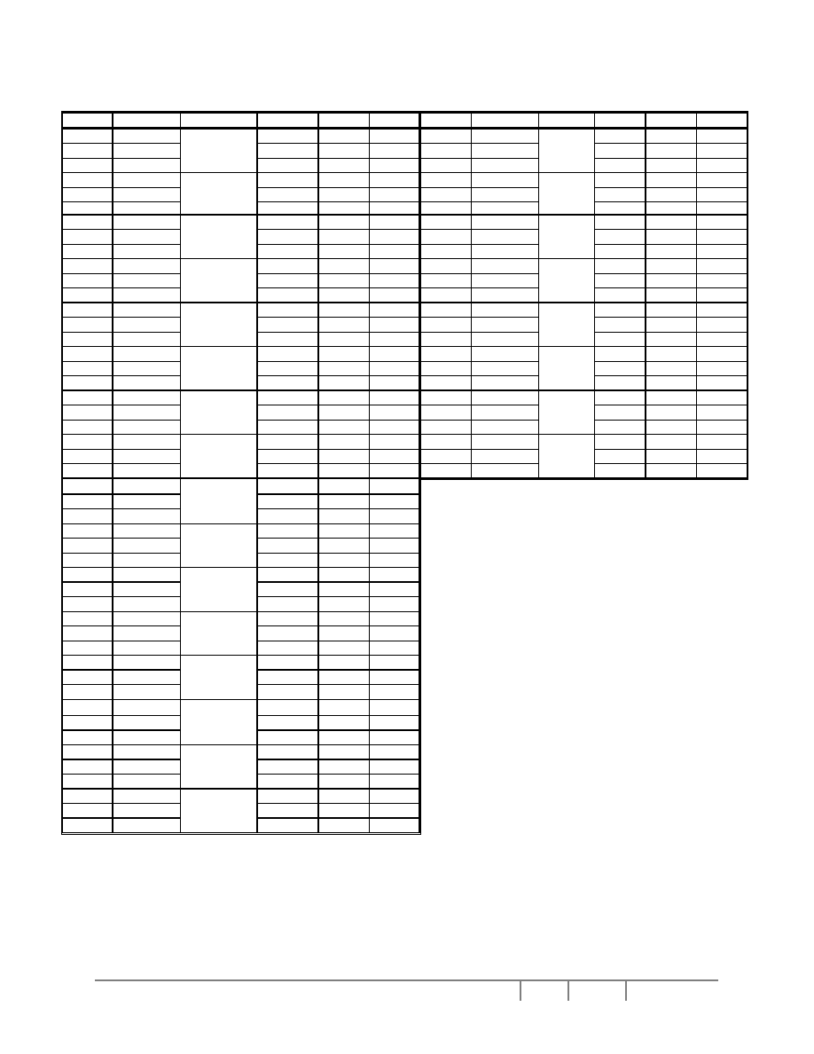
X
Y
Pad pitch
Pad # Pad Name
Signal
(
80
MUX68/
=
V
DD
) - 68mux
Signal
(
80
MUX68/
=
V
SS
) ≠ 80mux
X-pos Y-pos
585 ROW40
Non Select Signal
COM40 -6922.3
754.3
586 ROW41
Non Select Signal
COM41 -6965.7
754.3
587 ROW42
Non Select Signal
COM42 -7009.1
754.3
588 ROW43
Non Select Signal
COM43 -7052.5
754.3
589 ROW44
Non Select Signal
COM44 -7095.9
754.3
590 ROW45
Non Select Signal
COM45 -7139.3
754.3
591 ROW46
COM34
COM46
-7182.7
754.3
592 ROW47
COM35
COM47
-7226.1
754.3
593 ROW48
COM36
COM48
-7269.5
754.3
594 ROW49
COM37
COM49
-7312.9
754.3
595 ROW50
COM38
COM50
-7356.3
754.3
596 ROW51
COM39
COM51
-7399.7
754.3
597 ROW52
COM40
COM52
-7443.1
754.3
598 ROW53
COM41
COM53
-7486.5
754.3
599 ROW54
COM42
COM54
-7529.9
754.3
600 ROW55
COM43
COM55
-7573.3
754.3
601 ROW56
COM44
COM56
-7616.7
754.3
602 ROW57
COM45
COM57
-7660.1
754.3
603 ROW58
COM46
COM58
-7703.5
754.3
604 ROW59
COM47
COM59
-7746.9
754.3
605 ROW60
COM48
COM60
-7790.3
754.3
606 ROW61
COM49
COM61
-7833.7
754.3
607 ROW62
COM50
COM62
-7877.1
754.3
608 ROW63
COM51
COM63
-7920.5
754.3
609 ROW64
COM52
COM64
-7963.9
754.3
610 ROW65
COM53
COM65
-8007.3
754.3
611 ROW66
COM54
COM66
-8050.7
754.3
612 ROW67
COM55
COM67
-8094.1
754.3
613 ROW68
COM56
COM68
-8137.5
754.3
614 ROW69
COM57
COM69
-8180.9
754.3
615 ROW70
COM58
COM70
-8224.3
754.3
616 ROW71
COM59
COM71
-8267.7
754.3
617 ROW72
COM60
COM72
-8311.1
754.3
618 ROW73
COM61
COM73
-8354.5
754.3
619 ROW74
COM62
COM74
-8397.9
754.3
620 ROW75
COM63
COM75
-8441.3
754.3
621 ROW76
COM64
COM76
-8484.7
754.3
622 ROW77
COM65
COM77
-8528.1
754.3
623 ROW78
COM66
COM78
-8571.5
754.3
624 ROW79
COM67
COM79
-8614.9
754.3
625 ICONS
ICONS
ICONS
-8658.3
754.3
626 DUMMY
-8701.7
754.3
627 DUMMY
-8745.1
754.3
Bump Size
PAD#
X [um] Y [um] Pad pitch [um]
Pad 1-229
56
92
76.2
Pad 230 - 627 28
130
43.4

Solomon Systech
Sep 2003
P 12/61 Rev 1.00
SSD1770
6 PIN
DESCRIPTION
6.1
CS
This pin is the chip selection input. The chip is enabled for MCU communication only when CS is pulled
low.
6.2
RES
This pin is the reset signal input. Initialization of the chip is started once the reset pin is pulled low. The
minimum pulse width for reset sequence is 10us.
6.3 D/
C
This pin is Data/Command control pin. When the pin is pulled high, the input at D
7
-D
0
is treated as display
data. When the pin is pulled low, the input at D
7
-D
0
will be transferred to the command register.
6.4 R/
W
(
WR
)
This pin is MCU interface input. When 6800 interface mode is selected, this pin will be used as
Read/Write (
R/W
) selection input. Read mode will be carried out when this pin is pulled high and write
mode when this pin is pulled low.
When 8080 interface mode is selected, this pin is the Write (
WR
) control signal input. Data write
operation is initiated when this pin is pulled low and the chip is selected.
6.5 E(
RD
)
This pin is MCU interface input. When 6800 interface mode is selected, this pin will be used as the Enable
(E) signal. Read/ write operation is initiated when this pin is pulled high and the chip is selected.
When 8080 interface mode is selected, this pin is the Read (
RD
) control signal input. Data read operation
is initiated when this pin is pulled low and the chip is selected.
6.6 PS0 ≠ PS1
These pins are the bus interface mode selection input. Different bus interface can be selected changing
the setting of these pins.
PS1 PS0 MPU
Interface
L
H
8-bit 8080 parallel interface
H
H
8-bit 6800 parallel interface
H
L
3-lines serial peripheral interface (SPI) ≠ 9 bits SPI
L
L
4-lines serial peripheral interface (SPI)
Note1: For serial applications, D
0
≠ D
5
,
R/W ( WR )
,
E( RD )
are recommended to connect V
DD
.
Note2: Read back operation is only available in parallel mode
6.7
80
MUX68/
This pin is used to select the Mux ratio of the LCD driver. When
MUX68/( 80 )
is equal to V
DD
, COM0
~COM33 are mapped to ROW0~ROW33 and COM46~COM79 are mapped to ROW34~ROW67 of the
memory. When
MUX68/( 80 )
is equal to V
SS
, COM0~COM79 are mapped to ROW0~ROW79.
6.8 D
7
-D
0
These pins are the 8-bit bi-directional data bus in parallel interface mode. D
7
is the MSB while D
0
is the
LSB. When serial mode selected, D
7
is the serial data input SDA and D
6
is the serial clock input SCK.

SSD1770
Rev 1.00 P 13/61 Sep 2003
Solomon Systech
6.9 VL
REF
This pin is the ground of operation amplifier V
L4
and V
L5
. In normal power mode, it must connect to V
SS
. In
low power mode, it must connect to V
CI
and V
L4
must greater than 4V. Please refer to Figure 5 on page
20 for the detail.
6.10 VH
REF
This pin is the power supply pin of the operation amplifier V
L3
. It must connect to V
OUT
.
6.11 V
CIX2
This pin is internal reference pin. It must connect to V
CI
.
6.12 V
DD
This pin is the system power supply pin of the logic block.
6.13 V
DDIO
This pin is the system power supply pin of I/O buffer. Please refer to Figure 24 on page 59 for connection
example.
6.14 V
CI
This pin is the reference voltage input for internal DC-DC converter. The DC-DC converter output is
equals to the multiple factor (3X, 4X, 5X or 6X) times V
CI
with respect to V
SS
. The maximum output
voltage will limit the max. V
OUT
characteristic.
Note: Voltage at this input pin must be larger than or equal to V
DD
. (V
CI
V
DD
)
6.15 V
SS
This pin is the ground of logic.
6.16 RV
SS
This pin is the ground of Vref.
6.17 CV
SS
This pin is the ground of analog.
6.18 V
OUT
This is the most positive voltage supply pin of the chip. It can be supplied externally or generated by the
internal DC-DC converter. If the internal DC-DC converter generates the voltage level at V
OUT
, the voltage
level is used for internal referencing only. The voltage level at V
OUT
pin is not used for driving external
circuitry.

Solomon Systech
Sep 2003
P 14/61 Rev 1.00
SSD1770
6.19 V
L5,
V
L4,
V
L3
and V
L2
LCD driving voltages. They can be supplied externally or generated by the internal bias divider. They
have the following relationship:
V
OUT
> V
L5
> V
L4
> V
L3
> V
L2
> V
SS
Table 3 ≠ V
OUT
> V
L5
> V
L4
> V
L3
> V
L2
> V
SS
Relationship
1 : a bias
V
L5
(a-1)/a
*
V
OUT
V
L4
(a-2)/a * V
OUT
V
L3
2/a * V
OUT
V
L2
1/a * V
OUT
6.20 ROW0 ≠ ROW79
These pins provide the driving signals, COMMON, to the LCD panel.
6.21 COL0 ≠ COL311
These pins provide the LCD driving signals, SEGMENT, to the LCD panel. The Red, Green, Blue colors
signal are sent out from the SEGMENT output at the same time. The output voltage level of these pins is
V
DD
during sleep mode or standby mode.
6.22 ICON
This pin provides the driving signals, COMMON icon line.
6.23 CL
This pin is the system clock I/O. This pin is the external clock input for the device, which is enabled by
using extended command. It should be left open under normal operation. The internal oscillator will be
used after power on reset.
6.24 M
This pin is used for cascade purpose only. It should be left open under normal operation.
6.25 SYN
This pin is used for cascade purpose only. It should be left open under normal operation.
6.26 BUSY
This pin will be high during RAM buffer read/write operation and during graphic commands executing.
System programmer should read this pin (low is ready, high is busy) before sending next RAM buffer
related command (e.g. RAM write ≠ 5CH; RAM read ≠ 5DH OR any graphic commands)
6.27 TEST0~TEST17
These pins are used for internal only and should be left open, any connection is not allowed.
6.28 Dummy
There is a floating dummy pad without any internal circuitry connection.

SSD1770
Rev 1.00 P 15/61 Sep 2003
Solomon Systech
7 FUNCTIONAL BLOCK DESCRIPTIONS
7.1 Microprocessor Interface Logic
The Microprocessor Interface unit consists of three functional blocks for driving the 6800-series parallel
interface, 8080-series parallel interface, 3-lines serial peripheral interface and 4-lines serial peripheral
interface. The selection of different interface is done by PS0 to PS1 pins. Please refer to the pin
descriptions on page 12.
a) MPU Parallel 6800-series Interface
The parallel Interface consists of 8 bi-directional data pins (D
7
≠ D
0
), R/
W
, D/
C
, E,
CS
. R/
W
(
WR
) input high indicates a read operation from the Graphical Display Data RAM (GDDRAM) or
the status register. R/
W
input low indicates a write operation to Display Data RAM or Internal
Command Registers depending on the status of D/
C
input. The E input serves as data latch
signal (clock) when high provided that
CS
is low. Please refer to Figure 19to Figure 20 on page
54 to 55 for Parallel Interface Timing Diagram of 6800-series microprocessors. In order to match
the operating frequency of the GDDRAM with that of the MCU, some pipeline processing is
internally performed which requires the insertion of a dummy read before the first actual display
data read. This is shown in the following diagram.
Figure 3 ≠ Display Data
b) MPU Parallel 8080-series Interface
The parallel interface consists of 8 bi-directional data pins D
7
≠ D
0
,
RD
,
WR
,
D/ C
,
CS
.
RD
input
serves as data read latch signal (clock) when low provided that
CS
is low. Whether reading the
display data from GDDRAM or reading the status from the status register is controlled by
D/ C
.
WR
input serves as data write latch signal (clock) when low provided that
CS
is low. Whether
writing the display data to the GDDRAM or writing the command to the command register is
controlled by
D/ C
. A dummy read is also required before the first actual display data read for
8080-series interface.
c) MPU 4-lines Serial Peripheral Interface
The 4-lines serial peripheral Interface consists of serial clock SCK, serial data SDA,
D/ C
,
CS
.
SDA is shifted into 8-bit shift register on every rising edge of SCK in the order of data bit 7, data
bit 6 ...... data bit 0.
D/ C
is sampled on every eighth clock to determine whether the data byte in
the shift register is written to the Display Data RAM or command register at the same clock.
Please refer to Figure 21 on page 56 for serial interface timing.
write column address
dummy read
data read1
data read 2
data read 3
N
n
n+1
n+2
E( RD )
R/W ( WR )
DATA BUS

Solomon Systech
Sep 2003
P 16/61 Rev 1.00
SSD1770
d) MPU 3-lines Serial Peripheral Interface
The operation is similar to 4-lines serial peripheral interface while
D/ C
is not used. There are
altogether 9-bits will be shifted into the shift register on every ninth clock in sequence:
D/ C
bit, D
7
to D
0
bit. The
D/ C
bit (first bit of the sequential data) will determine the following data byte in the
shift register is written to the Display Data RAM (
D/ C
bit = 1) or the command register (
D/ C
bit =
0).
6800 ≠ series Parallel
Interface
8080 ≠ series Parallel
Interface
3-lines or 4-lines Serial
peripheral Interface
Data Read
8-bits
8-bits
No
Data Write
8-bits
8-bits
8-bits
Command Read
Status only
Status only
No
Command Write
Yes
Yes
Yes
Table 4 ≠ Data bus selection modes

SSD1770
Rev 1.00 P 17/61 Sep 2003
Solomon Systech
7.2 Reset
Circuit
This block is integrated into the Microprocessor Interface Logic which includes Power On Reset circuitry
and the hardware reset pin,
RES
. Both of these having the same reset function. Once the
RES
pin
receives a negative reset pulse, all internal circuitry will start to initialize. The minimum pulse width for
completing the reset sequence is 10us. The status of the chip after reset is given by:
When
RES
input is low, the chip is initialized to the following:
1.
Display
ON/OFF:
Display
is
OFF
2.
Normal/Inverse
Display:
Normal
Display
3. COM Scan Direction:
COM0 -> COM67/COM79
4.
Internal
Oscillator:
Disable
5. Reference Voltage Generation Circuit:
Disable
6. Voltage regulator and Voltage Follower:
Disable
7.
Booster
level:
6X
8. Bias ratio:
1/7(68 Mux) / 1/8 (80 Mux)
9.
Multiplex
ratio:
68
/
80
Mux
10.
Contrast
level:
32
11.
Internal
regulator
gain:
2.84
12. Average temperature gradient:
-0.2%/
o
C
13.
Partial
display
mode:
Disable
Start
COM
address:
0
End
COM
address:
0
14. Area Scroll set
Top
block
address:
0
Bottom
block
address:
0
Number of specified block:
0
Area scroll mode:
Whole screen scroll mode
15. Scroll start set
Start
block
address:
0
16. Data Scan Direction
Normal/inverse display of page address:
Normal
Normal/inverse display of column address:
Normal
Address-scan
direction:
Column
direction
RGB
arrangement:
RGB
Gray-scale
setup:
8
gray-scale
17. Start Page Address set:
0
18. End Page Address set:
0
19. Start Column address set:
0
20. End Column address set:
0
21. Select PWM/FRC
2-bit PWM + 2 bit FRC mode

Solomon Systech
Sep 2003
P 18/61 Rev 1.00
SSD1770
7.3 Command
Decoder
This module determines whether the input data is interpreted as data or command. Data is directed to this
module based upon the input of the
D/ C
pin. If
D/ C
pin is high, data is written to Graphic Display data
RAM (GDDRAM). If it is low, the input at D
7
≠ D
0
is interpreted as a Command and it will be decoded. The
decoded command will be written to the corresponding command register.
7.4 Graphic Display Data RAM (GDDRAM)
The GDDRAM is a bit mapped static RAM holding the bit pattern to be displayed. The size of the RAM is
312 (104 RGB) x 81 x 4 = 101088 bits. Figure 4 on page 19 is a description of the GDDRAM address
map. For mechanical flexibility, re-mapping on both Segment and Common outputs can be selected by
software. Please refer to the command "Data Output/Scan direction" in Table 5 on page 22 for detail
description.
Four pages of display data form a RAM address block and stored in the GDDRAM. Each block will form
the fundamental units of scrolling addresses. Various types of area scrolling can be performed by
software program according to the command "Set area Scroll" and "Set Scroll Start" in Table 11 on page
36.
In order to ease the access of the red, green and blue color data; the 8-bits color data (Red: 3 bits,
Green: 3 bits, Blue: 2 bits) is converted to 4-bits data (P10, P11, P12, P13). The 4-bits data are stored
into the GDDRAM such that the data are located in the appropriate RAM locations according to the gray
scale settings. Please refer to the description section of the command "Set Data Output/Scan Direction"
on page 22.

SSD1770
Rev 1.00 P 19/61 Sep 2003
Solomon Systech
each cell contains 4-bits data
COMMON
BLOCK PAGE
OUTPUT
0
COM0
1
COM1
2
COM2
3
COM3
4
COM4
5
COM5
6
COM6
7
COM7
8
COM8
9
COM9
10
COM10
11
COM11
:
:
:
:
:
:
:
:
:
:
:
:
:
:
:
:
:
:
:
:
:
:
:
:
:
:
:
:
:
:
:
:
:
:
:
:
:
:
:
:
:
:
:
:
:
64
COM64
65
COM65
66
COM66
67
COM67
68
COM68
69
COM69
70
COM70
71
COM71
72
COM72
73
COM73
74
COM74
75
COM75
76
COM76
77
COM77
78
COM78
79
COM79
20
ICON
ICON
......................
COL0
COL1
COL2
COL3
COL4
COL5
COL6
COL7
COL8
......................
COL303
COL304
COL305
COL306
COL307
COL308
COL309
COL310
COL311
Notes: Page and SEGMENT data scan direction depend on Data Output Scan Direction Setting.
Data Output Scan Directin setting cannot affect the Block scan direction.
SEG
0
Mapping depends
on COM Output
scan direction
setting
SEG
1
0
3
SEG
1
0
2
SEGMENT
COLUMN
DATA
0
1
2
16
SEG
1
SEG
2
SEG
1
0
1
17
18
19
Figure 4 ≠ Display Data RAM Map

Solomon Systech
Sep 2003
P 20/61 Rev 1.00
SSD1770
7.5 LCD Driving Voltage Generator and Regulator
This module generates the LCD voltage needed for display output. It takes a single supply input and
generates necessary bias voltages. It consists of:
1.
3X, 4X, 5X and 6X DC-DC voltage converter
2.
Bias Divider - If the output op-amp buffer option in Set Power Control Register command is enabled, this
circuit block will divide the regulator output (V
OUT
) to give the LCD driving levels (V
L2
≠ V
L5
).
The divider does not require external capacitors to reduce the external hardware and pin counts, power
configuration of op-amp is shown on below figure.
3.
Contrast Control ≠ Software control of 64 voltage levels of LCD voltage.
4.
Bias Ratio Selection circuitry ≠ Software control of 1/4 to 1/8 bias ratio to match the characteristic of LCD
panel.
5.
Self adjust temperature compensation circuitry ≠ Provide 4 different compensation grade selections to
satisfy the various liquid crystal temperature grades. The grading can be selected by software control.
Defaulted temperature coefficient (TC) value is ≠0.2%/∞C.
Figure 5 ≠ SSD1770 Hardware Configurations
V
OUT
VH
REF
V
DD
V
CI
V
CIX2
VL
REF
V
SS
+
+
SSD1770
Normal Power Mode
Recommended capacitance value:
C
1
: 1uF ~ 2.2uF
C
2
: 2.2uF ~ 4.7uF
C
1
C
2
V
OUT
VH
REF
V
DD
V
CI
V
CIX2
VL
REF
V
SS
+
+
SSD1770
Low Power Mode
In Low Power Mode, V
L4
must > 4V
Recommended capacitance value:
C
1
: 1uF ~ 2.2uF
C
2
: 2.2uF ~ 4.7uF
C
1
C
2
SSD1770
Rev 1.00 P 21/61 Sep 2003
Solomon Systech
7.6 Oscillator
Circuit
This module is an On-Chip low power RC oscillator circuitry (Figure 6). The oscillator generates the clock
for the DC-DC voltage converter. This clock is also used in the Display Timing Generator.
Figure 6 ≠ Oscillator structural block diagram
7.7 Display Data Latch
This block is a series of latches carrying the display signal information. These latches hold the data, which
will be fed to the HV Buffer Cell and Level Selector to output the required voltage level.
7.8 HV Buffer Cell (Level Shifter)
This block is embedded in the Segment/Common Driver Circuits. HV Buffer Cell works as a level shifter,
which translates the low voltage output signal to the required driving voltage. The output is shifted out with
reference to the internal FRM clock, which comes from the Display Timing Generator. The voltage levels
are given by the level selector, which is synchronized with the internal M signal.
7.9 Level
Selector
This block is embedded in the Segment/Common Driver circuits. Level Selector is a control of the display
synchronization. Display voltage levels can be separated into two sets and used with different cycles.
Synchronization is important since it selects the required LCD voltage level to the HV Buffer Cell, which in
turn outputs the COM or SEG LCD waveform.
enable
Oscillation Circuit
enable
Buffer
Internal resistor
OSC2
OSC1
Oscillator
enable
(CL)

Solomon Systech
Sep 2003
P 22/61 Rev 1.00
SSD1770
8 COMMAND
TABLE
Table 5 ≠ COMMAND TABLE (D/
C
= 0, R/
W
(
WR
) = 0, E=1(
RD
= 1) unless specific setting is stated)
Bit Pattern
Command
Description
(
C
/
D
= 0) 00010101
(
C
/
D
= 1) X
7
X
6
X
5
X
4
X
3
X
2
X
1
X
0
(
C
/
D
= 1) Y
7
Y
6
Y
5
Y
4
Y
3
Y
2
Y
1
Y
0
Set Column
Address
Set the start column address by X
7
X
6
X
5
X
4
X
3
X
2
X
1
X
0
Set the end column address by Y
7
Y
6
Y
5
Y
4
Y
3
Y
2
Y
1
Y
0.
Column address = 00000000b (POR)
In 8-levels gray scale mode, column address is in a range of 0~103.
In 16-level gray scale mode, column address is in a range of 0~51.
(
C
/
D
= 0) 01110101
(
C
/
D
= 1) X
7
X
6
X
5
X
4
X
3
X
2
X
1
X
0
(
C
/
D
= 1) Y
7
Y
6
Y
5
Y
4
Y
3
Y
2
Y
1
Y
0
Set Page Address
Set the start page address by X
7
X
6
X
5
X
4
X
3
X
2
X
1
X
0
Set the end page address by Y
7
Y
6
Y
5
Y
4
Y
3
Y
2
Y
1
Y
0.
Page address = 00000000b (POR)
(
C
/
D
= 0) 10111011
(
C
/
D
= 1) *****X
2
X
1
X
0
Set COM Output
Scan Direction
80
/
68
MUX
= V
SS
X
2
X
1
X
0
ROW0..ROW33 ROW34..ROW39 ROW40..ROW45 ROW46..ROW79
0 0 0
COM0->COM33 COM34->COM39 COM40->COM45 COM46->COM79 (POR)
0 0 1
COM0->COM33 COM34->COM39 COM79<-COM64 COM63<-COM40
0 1 0
COM39<-COM6 COM5<-COM0 COM40->COM45 COM46->COM79
0 1 1
COM39<-COM6 COM5<-COM0 COM79<-COM64 COM63<-COM40
80
/
68
MUX
= V
DD
X
2
X
1
X
0
ROW0..ROW33 ROW34..ROW39 ROW40..ROW45 ROW46..ROW79
0 0 0
COM0->COM33 NON SELECT OUTPUT COM34->COM67 (POR)
0 0 1
COM0->COM33 NON SELECT OUTPUT COM67<-COM34
0 1 0
COM33<-COM0 NON SELECT OUTPUT COM34->COM67
0 1 1
COM33<-COM0 NON SELECT OUTPUT COM67<-COM34
(
C
/
D
= 0) 10111100
(
C
/
D
= 1) *****P12 P11 P10
(
C
/
D
= 1) *****P22 P21 P20
(
C
/
D
= 1) *****P32 P31 P30
Set Data Output
Scan Direction
a) Normal or Reverse page/column/scan directions
P10 = 0: set page address to normal display (POR)
P10 = 1: set page address to inverse display
P11 = 0: set column address to normal rotation (POR)
P11 = 1: set column address to inverse rotation
P12 = 0: set scan direction to column scan (POR)
P12 = 1: set scan direction to page scan
Please refer to the Figure 9 on page 33 for detail description of
column/page scan direction modes
b) RGB color arrangement
P22, P21, P20: The control bits are used for setting the (RGB) color
arrangement of segment output, 000 is POR value. Please refer to the
Figure 10 on page 34 for detail mapping of the segment output.
c) Gray-scale selection
P32 P31 P30
Gray-scale modes
0 0 1 8-levels gray scale mode (POR)
0 1 0 16-levels gray scale mode (Type A)
Please refer to the Table 12 on page 27 to Table 15 on page 30 for
detail description of different gray-scale selection modes.
Remarks: "*" denote DON'T CARE bit

SSD1770
Rev 1.00 P 23/61 Sep 2003
Solomon Systech
Remarks: "*" denote DON'T CARE bit
Bit Pattern
Command
Description
(
C
/
D
= 0) 11001110
(
C
/
D
= 1) **** X
31
X
21
X
11
X
01
(
C
/
D
= 1) **** X
32
X
22
X
12
X
02
:
:
(
C
/
D
= 1) **** X
38
X
28
X
18
X
08
(
C
/
D
= 1) **** X
39
X
29
X
19
X
09
:
:
(
C
/
D
= 1) ****X
316
X
216
X
116
X
016
(
C
/
D
= 1) ****X
317
X
217
X
117
X
017
:
:
(
C
/
D
= 1) ****X
320
X
220
X
120
X
020
Set Color Look Up
Table
N DB
3
DB
2
DB
1
DB
0
color position
1 X
3N
X
2N
X
1N
X
0N
Intermediate red tone 000
2 X
3N
X
2N
X
1N
X
0N
Intermediate red tone 001
: :
: :
8 X
3N
X
2N
X
1N
X
0N
Intermediate red tone 111
9 X
3N
X
2N
X
1N
X
0N
Intermediate green tone 000
: :
: :
16 X
3N
X
2N
X
1N
X
0N
Intermediate green tone 111
17 X
3N
X
2N
X
1N
X
0N
Intermediate blue tone 00
: :
: :
20 X
3N
X
2N
X
1N
X
0N
Intermediate blue tone 11
(
C
/
D
= 0) 11001010
(
C
/
D
= 1) 00000000
(
C
/
D
= 1) ** Y
5
Y
4
Y
3
Y
2
Y
1
Y
0
(
C
/
D
= 1) 00000000
Set Display Control
Driver duty selection
Select driver duty from 1 / 8 to 1 / 80. As Y
5
Y
4
Y
3
Y
2
Y
1
Y
0
is increased
from 000001b to 010011b, the number of display lines, N is increased
at the same rating. To specify the Y
5
Y
4
Y
3
Y
2
Y
1
Y
0,
1
4
N
Y
~
Y
0
5
-
=
(
C
/
D
= 0) 10101010
(
C
/
D
= 1) ** X
5
X
4
X
3
X
2
X
1
X
0
(
C
/
D
= 1) ** Y
5
Y
4
Y
3
Y
2
Y
1
Y
0
(
C
/
D
= 1) ** Z
5
Z
4
Z
3
Z
2
Z
1
Z
0
(
C
/
D
= 1) ****** P41 P40
Set Area Scroll
a) Top Block Address
X
5
X
4
X
3
X
2
X
1
X
0
is used to specify the block address (1 block = 4 lines) at
the top of the scrolling area.
Top block address = 000000b (POR)
b) Bottom Block Address
Y
5
Y
4
Y
3
Y
2
Y
1
Y
0
is used to specify the block address (1 block = 4 lines) at
the bottom of the scrolling area.
Bottom block address = 000000b (POR)
c) Number of specified Blocks
The number of specified blocks = Number of (Top fixed area + Scroll
area) blocks ≠1. If bottom scroll or whole screen scroll mode is chosen,
the number of specified blocks is set to Z
5
~Z
0
Number of specified blocks = 000000b (POR)
d) Area Scroll Mode
There are four types of area scroll.
P41 P40
Types of Area Scroll
0 0 Center Screen Scroll
0 1 Top Screen Scroll
1 0 Bottom Screen Scroll
1 1 Whole Screen Scroll
Type of area scroll = Whole Screen Scroll (POR)
(
C
/
D
= 0) 10101011
(
C
/
D
= 1) ** X
5
X
4
X
3
X
2
X
1
X
0
Set Scroll Start
X
5
X
4
X
3
X
2
X
1
X
0
specify the start block address
(1 block = 4 lines) of area scrolling.
Start block address = 000000b (POR)

Solomon Systech
Sep 2003
P 24/61 Rev 1.00
SSD1770
Remarks: "*" denote DON'T CARE bit
Bit Pattern
Command
Description
(
C
/
D
= 0) 00100000
(
C
/
D
= 1) ****X
3
X
2
X
1
X
0
Set Power Control
Register
X
0
=0: turns off the reference voltage generator (POR)
X
0
=1: turns on the reference voltage generator
X
1
=0: turns off the internal regulator and voltage follower (POR)
X
1
=1: turns on the internal regulator and voltage follower
Select booster level
X
3
X
2
Boost level
0 0 3X
0 1 4X
1 0 5X
1 1 6X (POR)
(
C
/
D
= 0) 10000001
(
C
/
D
= 1) ** X
5
X
4
X
3
X
2
X
1
X
0
(
C
/
D
= 1) ***** Y
2
Y
1
Y
0
Set Contrast Level
& Internal
Regulator Resistor
Ratio
a) Select contrast level from 64 contrast steps
Contrast increases as X
5
X
4
X
3
X
2
X
1
X
0
is increased from 000000b to
111111b. X
5
X
4
X
3
X
2
X
1
X
0
= 000000b (POR)
b) The internal regulator gain (1+R
2
/R
1
) V
OUT
increases as Y
2
Y
1
Y
0
is
increased from 000b to 111b. The factor, 1+R
2
/R
1
, is given by:
Y
2
Y
1
Y
0
= 000: 2.84 (POR)
Y
2
Y
1
Y
0
= 001: 3.71
Y
2
Y
1
Y
0
= 010: 4.57
Y
2
Y
1
Y
0
= 011: 5.44
Y
2
Y
1
Y
0
= 100: 6.30
Y
2
Y
1
Y
0
= 101: 7.16
Y
2
Y
1
Y
0
= 110: 8.03
Y
2
Y
1
Y
0
= 111: 8.89
(
C
/
D
= 0) 1101011X
0
Set Increment /
Decrement of the
contrast
X
0
=0: The contrast set of voltage regulator is incremented by 1
X
0
=1: The contrast set of voltage regulator is decremented by 1
(
C
/
D
= 0) 1010011X
0
Set Normal/Inverse
Display
X
0
=0: normal display (POR)
X
0
=1: inverse display
(
C
/
D
= 0) 10101000
(
C
/
D
= 1) *X
6
X
5
X
4
X
3
X
2
X
1
X
0
(
C
/
D
= 1) *Y
6
Y
5
Y
4
Y
3
Y
2
Y
1
Y
0
Enter partial
Display
X
6
X
5
X
4
X
3
X
2
X
1
X
0
: Start COM Address = 000000b (POR)
Y
6
Y
5
Y
4
Y
3
Y
2
Y
1
Y
0
: End COM Address = 000000b (POR)
(
C
/
D
= 0) 10101001
Exit partial Display
Exit the "partial display mode" by executing the command 10101001b
(POR)
(
C
/
D
= 0) 1010111X
0
Set Display On/Off
X
0
=0: turns off LCD panel (POR)
X
0
=1: turns on LCD panel
(
C
/
D
= 0) 1001010X
0
Enter/Exit sleep
mode
X
0
=0: exit the sleep mode.
X
0
=1: enter sleep mode. (POR)
(
C
/
D
= 0) 110100 X
1
X
0
Enable/disable
internal oscillator
X
1
X
0
Internal oscillator status
0 1 ON
1 0 OFF (POR)
(
C
/
D
= 0) 10000010
(
C
/
D
= 1) ****** X
1
X
0
Set Temperature
compensation
coefficient
Average temperature gradients
X
1
X
0
Average Temperature Gradient [%/
o
C]
0 0 -0.10
0 1 -0.15
1 0 -0.20(POR)
1 1 -0.25
(
C
/
D
= 0) 00100101
NOP
Command result in No Operation
The command should be issued after the execution of the Status Read
command
(
C
/
D
= 0) 01011100
(
C
/
D
= 1)
Y
71
Y
61
Y
51
Y
41
Y
31
Y
21
Y
11
Y
01
Write display data
Enter the "write display data mode " by executing the command
01011100b. The following byte is used to specify the data byte to be
written to the GDDRAM directly.
The
C
/
D
bit should be stated at logic "1" during the display data is
written to the GDDRAM.

SSD1770
Rev 1.00 P 25/61 Sep 2003
Solomon Systech
Graphic command table
-
Remarks: "*" denote DON'T CARE bit
- After executed the graphic command, waiting time is required for update GDDRAM content. (When V
DD
= 2.4 ~ 3.6, waiting time = 125 ns/pixel.)
Bit Pattern
Command
Description
(
C
/
D
= 0) 01011101
(
C
/
D
= 1 &
W
/
R
= 1)
********
Y
71
Y
61
Y
51
Y
41
Y
31
Y
21
Y
11
Y
01
Read display data
Enter the "read display data mode " by executing the command
01011100b. The next byte is a dummy data. The GDDRAM data will be
read form the second byte. The GDDRAM column address pointer will
be increased by one automatically after each data read (8-levels gray
scale mode) OR after each 3-bytes data read. (16-levels gray scale
mode).
Bit Pattern
Command
Description
(
C
/
D
= 0) 10000011
(
C
/
D
= 1) A
7
A
6
A
5
A
4
A
3
A
2
A
1
A
0
(
C
/
D
= 1) B
7
B
6
B
5
B
4
B
3
B
2
B
1
B
0
(
C
/
D
= 1)C
7
C
6
C
5
C
4
C
3
C
2
C
1
C
0
(
C
/
D
= 1)D
7
D
6
D
5
D
4
D
3
D
2
D
1
D
0
(
C
/
D
= 1)R
3
R
2
R
1
R
0
G
3
G
2
G
1
G
0
(
C
/
D
= 1) ****B
3
B
2
B
1
B
0
Draw Line
Enter the "Draw line mode" by executing the command 10000011. The
following four bytes (A
0
to A
7
, B
0
to B
7
, C
0
to C
7
, D
0
to D
7
) are used to
specify the start coordinates of X address, start coordinates of Y
address, end coordinates or X address and the end coordinates of Y
address. The remaining two bytes are used to specify the color.
Remarks: A
103; B
79; C
103; D
79
(
C
/
D
= 0) 10010010
(
C
/
D
= 1) *******A
0
Fill Enable/Disable
Enter the "Fill Enable/Disable mode" by executing the command
10010010.
A
0
=0: Filled color option is disabled (POR)
A
0
=1: Filled color option is enabled
(
C
/
D
= 0) 10000100
(
C
/
D
= 1) A
7
A
6
A
5
A
4
A
3
A
2
A
1
A
0
(
C
/
D
= 1) B
7
B
6
B
5
B
4
B
3
B
2
B
1
B
0
(
C
/
D
= 1) C
7
C
6
C
5
C
4
C
3
C
2
C
1
C
0
(
C
/
D
= 1) D
7
D
6
D
5
D
4
D
3
D
2
D
1
D
0
(
C
/
D
=1) R
3
R
2
R
1
R
0
G
3
G
2
G
1
G
0
(
C
/
D
=1) ****B
3
B
2
B
1
B
0
(
C
/
D
=1) R
3
R
2
R
1
R
0
G
3
G
2
G
1
G
0
(
C
/
D
=1) ****B
3
B
2
B
1
B
0
Draw rectangle
Enter the "Draw rectangle mode" by executing the command
10000100. The following four bytes (A
0
to A
7
, B
0
to B
7
, C
0
to C
7
, D
0
to
D
7
) are used to specify the start coordinates of X address, start
coordinates of Y address, end coordinates or X address and the end
coordinates of Y address. The next two bytes are used to specify the
color. The last two bytes are used to specify the fill color.
Remarks: A
C; B
D; C
103; D
79
(
C
/
D
= 0) 10001010
(
C
/
D
= 1) A
7
A
6
A
5
A
4
A
3
A
2
A
1
A
0
(
C
/
D
= 1) B
7
B
6
B
5
B
4
B
3
B
2
B
1
B
0
(
C
/
D
= 1) C
7
C
6
C
5
C
4
C
3
C
2
C
1
C
0
(
C
/
D
= 1) D
7
D
6
D
5
D
4
D
3
D
2
D
1
D
0
(
C
/
D
= 1) E
7
E
6
E
5
E
4
E
3
E
2
E
1
E
0
(
C
/
D
= 1) F
7
F
6
F
5
F
4
F
3
F
2
F
1
F
0
Copy
Enter the "Copy mode" by executing the command. The following four
bytes (A
0
to A
7
, B
0
to B
7
, C
0
to C
7
, D
0
to D
7
) are used to specify the
start coordinates of X address, start coordinates of Y address, end
coordinates or X address and the end coordinates of Y address. The
remaining two bytes (E
0
to E
7
, F
0
to F
7
) are used to specify the new
location of X coordinates and Y coordinates.
Remarks: A
C; B
D; C
103; D
79
(
C
/
D
= 0) 10001100
(
C
/
D
= 1) A
7
A
6
A
5
A
4
A
3
A
2
A
1
A
0
(
C
/
D
= 1) B
7
B
6
B
5
B
4
B
3
B
2
B
1
B
0
(
C
/
D
= 1) C
7
C
6
C
5
C
4
C
3
C
2
C
1
C
0
(
C
/
D
= 1) D
7
D
6
D
5
D
4
D
3
D
2
D
1
D
0
Dim Window
Enter the "Dim Window mode" by executing the command 10001100.
The following four bytes (A
0
to A
7
, B
0
to B
7
, C
0
to C
7
, D
0
to D
7
) are used
to specify the start coordinates of X address, start coordinates of Y
address, end coordinates or X address and the end coordinates of Y
address. The selected window area will be dimmed by 75% white.
Remarks: A
C; B
D; C
103; D
79
(
C
/
D
= 0) 10001110
(
C
/
D
= 1) A
7
A
6
A
5
A
4
A
3
A
2
A
1
A
0
(
C
/
D
= 1) B
7
B
6
B
5
B
4
B
3
B
2
B
1
B
0
(
C
/
D
= 1) C
7
C
6
C
5
C
4
C
3
C
2
C
1
C
0
(
C
/
D
= 1) D
7
D
6
D
5
D
4
D
3
D
2
D
1
D
0
Clear Window
Enter the "Clear Window mode" by executing the command 10001110.
The following four bytes (A
0
to A
7
, B
0
to B
7
, C
0
to C
7
, D
0
to D
7
) are used
to specify the start coordinates of X address, start coordinates of Y
address, end coordinates or X address and the end coordinates of Y
address. All GDDRAM content will be set to 0.
Remarks: A
C; B
D; C
103; D
79

Solomon Systech
Sep 2003
P 26/61 Rev 1.00
SSD1770
Extended command table
Bit Pattern
Command
Description
(
C
/
D
= 0) 1111 1011
(
C
/
D
= 1) ****0B
2
B
1
B
0
Set biasing ratio
Allow user to set bias from 1/ 4 to 1/8
B
2
B
1
B
0
Bias ratio
0 0 0 1/4 bias
0 0 1 1/5 bias
0 1 0 1/6 bias
0 1 1 1/7 bias (POR, if 68 Mux)
1 0 0 1/8 bias (POR, if 80 Mux)
1 0 1 reserved
1 1 X reserved
(
C
/
D
= 0) 1111 0010
(
C
/
D
= 1) 0000 F
3
F
2
F
1
F
0
(
C
/
D
= 1) x00N
4
N
3
N
2
N
1
N
0
Set Frame
frequency and N-
line Inversion
This command uses to change the frame frequency and set the N-
line inversion.
68 Mux operation 80 Mux operation
F
3
F
2
F
1
F
0
F
3
F
2
F
1
F
0
1 1 1 1 : 110 Hz 1 1 1 1 : 93.5 Hz
1 1 1 0 : 102.5 Hz 1 1 1 0 : 87 Hz
1 1 0 1 : 97.5 Hz 1 1 0 1 : 82.5 Hz
1 1 0 0 : 92 Hz 1 1 0 0 : 78 Hz
1 0 1 1 : 88.5 Hz 1 0 1 1 : 75 Hz
1 0 1 0 : 84 Hz 1 0 1 0 : 71.5 Hz
1 0 0 1 : 81 Hz 1 0 0 1 : 69 Hz
1 0 0 0 : 78 Hz (POR) 1 0 0 0 : 66 Hz (POR)
0 1 1 1 : 76 Hz 0 1 1 1 : 64.5 Hz
0 1 1 0 : 73 Hz 0 1 1 0 : 62 Hz
0 1 0 1 : 70.5 Hz 0 1 0 1 : 60 Hz
0 1 0 0 : 68 Hz 0 1 0 0 : 58 Hz
0 0 1 1 : 66 Hz 0 0 1 1 : 56 Hz
0 0 1 0 : 64 Hz 0 0 1 0 : 54.5 Hz
0 0 0 1 : 62 Hz 0 0 0 1 : 53 Hz
0 0 0 0 : 60 Hz 0 0 0 0 : 51 Hz
The second byte data sets the n-line inversion register from 2 to 32
lines to reduce display crosstalk. Register values from 00001b to
11111b are mapped to 2 lines to 32 lines respectively. Value
00000b disables the N-line inversion. 00110 is the POR value.
To avoid a fix polarity at some lines, it should be noted that the
total number of mux (including the icon line) should NOT be a
multiple of the lines of inversion (n).
(
C
/
D
= 0) 1010001X
0
Enable/disable icon X
0
=0: Disable icon row (POR)
X
0
=1: Enable icon row
(
C
/
D
= 0) 1111 0111
(
C
/
D
= 1) 0010 1000
(
C
/
D
= 1) 0010 11X
1
X
0
(
C
/
D
= 1) **** 0101
Select PWM/FRC
4 bits PWM/FRC or 2 bits PWM + 2 bits FRC selection
X
1
X
0
0 0 : 4 bits PWM
0 1 : 4 bits FRC
1 0 : 2 bits PWM + 2 bits FRC (POR)
1 1 : Reserved
Remarks: "*" denote DON'T CARE bit

SSD1770
Rev 1.00 P 27/61 Sep 2003
Solomon Systech
Bit Pattern
Command
Description
(
C
/
D
= 0) 1111 0110
(
C
/
D
= 1) 0001 X
3
X
2
X
1
X
0
(
C
/
D
= 1) 0000 1010
OTP setting
This command set the offset value of contrast
X
3
X
2
X
1
X
0
0000 : original contrast
0001 : original contrast + 2 step
0010 : original contrast + 4 steps
0011 : original contrast + 6 steps
0100 : original contrast + 8 steps
0101 : original contrast + 10 steps
0110 : original contrast + 12 steps
0111 : original contrast + 14 steps
1000 : original contrast - 16 steps
1001 : original contrast - 14 steps
1010 : original contrast - 12 steps
1011 : original contrast - 10 steps
1100 : original contrast - 8 steps
1101 : original contrast - 6 steps
1110 : original contrast - 4 steps
1111 : original contrast - 2 step
(
C
/
D
= 0) 1111 1000
OTP programming
This command start to program LCD driver with OTP offset value.
Each bit can be programmed to 1 once. Detail of OTP
programming procedure on page 46
Remarks: "*" denote DON'T CARE bit
Solomon Systech
Sep 2003
P 28/61 Rev 1.00
SSD1770
Table 6 - Read Command Table
Bit Pattern
Command
Description
(
C
/
D
= 0 &
W
/
R
= 0)
01011101
(
C
/
D
= 0 &
W
/
R
= 1)
D
7
D
6
* D
4
D
3
D
2
D
1
D
0
Status Register
Read
D
7
D
6
= 00: Center Screen Scroll Mode
D
7
D
6
= 01: Top Screen Scroll Mode
D
7
D
6
= 10: Bottom Screen Scroll Mode
D
7
D
6
= 11: Whole Screen Scroll Mode
D
4
= 0: Scan Direction is column direction
D
4
= 1: Scan Direction is page direction
D
3
= 0: Display is OFF
D
3
= 1: Display is ON
D
2
= 0: Sleep Mode is disabled
D
2
= 1: Sleep Mode is enabled
D
1
= 0: Display is Inverse
D
1
= 1: Display is Normal
D
0
= 0: Partial display is disabled
D
0
= 1: Partial display is enabled
Note: Command patterns other than that given in Command Table are prohibited. Otherwise, unexpected result will
occur.
Remarks: "*" denote DON'T CARE bit

SSD1770
Rev 1.00 P 29/61 Sep 2003
Solomon Systech
8.1 Data Read / Write
To read data from the GDDRAM, 5Dhex command should be executed then input High to
R/W ( WR )
pin and
D/ C
pin for 6800-series parallel mode. Low to E(
RD
) pin and High to
D/ C
pin for 8080-series
parallel mode. No data read is provided for serial mode. In normal mode, GDDRAM column address
pointer will be increased by one automatically after each data read in 8-levels gray scale mode OR
after each 3-bytes data read in 16-levels gray scale mode. Also, a dummy read is required before the
first data is read. See Figure 3 in Functional Description.
To write data to the GDDRAM, input Low to
R/ W ( WR )
pin and High to
D/ C
pin for 6800-series
parallel mode. For serial interface, it will always be in write mode. GDDRAM column address pointer
will be increased by one automatically after each data write in 8-levels gray scale mode OR each 3-
bytes data write in 16-levels scale mode. The address will be reset to 0 in next data read/write
operation is executed when it is 103.

Solomon Systech
Sep 2003
P 30/61 Rev 1.00
SSD1770
R G B
R G B
R G B
R G B
R G B
R G B
Page
Data
COMMON
OUTPUTS
BLOCK P10 = 0 P10 = 1
0
79
COM0
1
78
COM1
2
77
COM2
3
76
COM3
4
75
COM4
5
74
COM5
6
73
COM6
7
72
COM7
:
:
:
:
:
:
:
:
:
:
:
:
:
:
:
:
:
:
:
:
:
:
:
:
:
:
:
:
:
:
:
:
:
:
:
:
:
:
:
:
:
:
:
:
:
68
11
COM68
69
10
COM69
70
9
COM70
71
8
COM71
72
7
COM72
73
6
COM73
74
5
COM74
75
4
COM75
76
3
COM76
77
2
COM77
78
1
COM78
79
0
COM79
20
ICON
ICON
ICON
COL0
COL1
COL2
COL3
COL4
COL5
COL6
COL7
COL8
COL9
CO
L10
CO
L11 ...........
CO
L306
CO
L307
CO
L308
CO
L309
CO
L310
CO
L311
101
103
0
1
SEGMENT
OUTPUTS
19
LCD Read
Direction
17
18
D4
D3
D2
D1
D0
2
3
RGB Alignment using 8-levels gray scale mode
Column
P11 = 0
Color
P11 = 1
103
102
101
100
1
D4
D3
D2
D1
D0
0
1
D7
D6
D5
D4
D3
D2
D1
D0
D7
D6
D5
D1
D0
D7
D6
D5
0
D7
D6
D5
D4
D3
D2
D1
D0
D7
D6
D5
D4
D3
D2
D1
D0
D7
D6
D5
D4
D3
D2
9 COMMAND
DESCRIPTIONS
9.1 Set Column Address
This command specifies the 8-bit column address of the display data RAM. The start and the end column
address are specified by this command. The driver supports up to 104 columns. As the addresses are
incremented from the start column to the end column in the column direction scan, the page address is
automatically incremented by 1. The column address is then returned to the start column. The column
address will be increased by each data access after it is preset by the MCU. Start column < End column
must be maintained.
Table 7 - RAM arrangements of 8-levels gray scale mode

SSD1770
Rev 1.00 P 31/61 Sep 2003
Solomon Systech
R1 G1 B1 R2 G2 B2 R1 G1 B1 R2 G2 B2
R1 G1 B1 R2 G2 B2
Page
Data D7
D6
D5
D4
D3
D2
D1
D0
D7
D6
D5
D4
D3
D2
D1
D0
D7
D6
D5
D4
D3
D2
D1
D0
D7
D6
D5
D4
D3
D2
D1
D0
D7
D6
D5
D4
D3
D2
D1
D0
D7
D6
D5
D4
D3
D2
D1
D0
D7
D6
D5
D4
D3
D2
D1
D0
D7
D6
D5
D4
D3
D2
D1
D0
D7
D6
D5
D4
D3
D2
D1
D0
R2 G2 B2 R1 G1 B1 R2 G2 B2 R1 G1 B1
R2 G2 B2 R1 G1 B1
Page
Data
COMMON
OUTPUTS
BLOCK
P10 = 0 P10 = 1
0
79
COM0
1
78
COM1
2
77
COM2
3
76
COM3
4
75
COM4
5
74
COM5
6
73
COM6
7
72
COM7
:
:
:
:
:
:
:
:
:
:
:
:
:
:
:
:
:
:
:
:
:
:
:
:
:
:
:
:
:
:
:
:
:
:
:
:
:
:
:
:
:
:
:
:
:
68
11
COM68
69
10
COM69
70
9
COM70
71
8
COM71
72
7
COM72
73
6
COM73
74
5
COM74
75
4
COM75
76
3
COM76
77
2
COM77
78
1
COM78
79
0
COM79
20
ICON
ICON
ICON
COL
0
COL
1
COL
2
COL
3
COL
4
COL
5
COL
6
COL
7
COL
8
COL
9
C
O
L10
C
O
L11 ...........
C
O
L306
C
O
L307
C
O
L308
C
O
L309
C
O
L310
C
O
L311
D7
D6
D5
D4
1
D3
D2
D1
D0
D7
D6
D5
D4
D3
D2
D1
D0
D3
D2
D1
D0
D7
D6
D5
D4
D3
D2
D1
D0
D7
D6
D5
D4
D3
D2
D1
D0
D7
D6
D5
D4
RGB Alignment using 16-levels gray scale mode
Column
P11 = 0
Color
1
1
19
LCD Read
Direction
P11 = 1
Color
17
18
D3
D2
D1
D0
D7
D6
D5
D4
0
51
51
SEGMENT
OUTPUTS
D3
D2
D1
D0
D7
D6
D5
D4
D7
D6
D5
D4
D3
D2
D1
D0
D7
D6
D5
D4
D3
D2
D1
D0
0
0
0
0
51
51
50
50
} }
} }
Table 8 - RAM arrangements of 16-levels gray scale mode

Solomon Systech
Sep 2003
P 32/61 Rev 1.00
SSD1770
9.2 Set Page Address
This command enters the page address from 0 to 79 to the RAM page register for read/write operations.
The driver supports up to 80 lines. All in all, there are 80 pages. As the addresses are incremented from
the start page to the end page in the page direction scan, the column address is incremented by 1. The
page address is then returned to the start page. Start page < End page must be maintained.
9.3 Set COM Output Scan Direction
This command sets the scan direction of the COM output allowing layout flexibility in LCD module
assembly. Please refer to the Table 5 on Page 22 for detail mapping. In addition, the display will have
immediate effect once this command is issued. That is, if this command is sent during normal display, the
graphic display will have vertical flipping effect.
9.4 Set Data Output Scan Direction
This command sets the DDRAM such that the MPU operates the display data in the internal RAM.
A. Normal or Inverse page/column/scan directions
The Data Scan direction can be set to either normal or inverse display page and column address scan
direction. The column and the page direction are illustrated in the Figure 7 on page 32.
80
/
68
MUX
= 0
P12 = 0: Column Direction
P11=0 0
1
2
101
102
103
P11=1 103
102
101
2
1
0
P10=0
P10=1
0 79
1 78
2 77
:
:
:
:
:
:
:
:
:
77 2
78 1
79 0
P12 = 1: Page Direction
P11=0 0
1
2
101
102
103
P11=1 103
102
101
2
1
0
P10=0
P10=1
0 79
1 78
2 77
:
:
:
:
:
:
:
:
:
77 2
78 1
79 0
Figure 7 - column and page scan direction of 8-level gray scale mode
SSD1770
Rev 1.00 P 33/61 Sep 2003
Solomon Systech
80
/
68
MUX
= 0
P12 = 0: Column Direction
P11=0 0
0
1 50
51
51
P11=1 51
51
50 1
0
0
P10=0
P10=1
0 79
1 78
2 77
:
:
:
:
:
:
:
:
:
77 2
78 1
79 0
P12 = 1: Page Direction
P11=0 0
0
1 50
51
51
P11=1 51
51
50 1
0
0
P10=0
P10=1
0 79
1 78
2 77
:
:
:
:
:
:
:
:
:
77 2
78 1
79 0
Figure 8 - column and page scan direction of 16-level gray scale mode
Figure 9 ≠ Example of Normal or Reverse page/column/ scan directions
P10 = 0
P10 = 1
P10 = 0
P10 = 1
P11 = 0
P11 = 0
P11 = 1
P11 = 1
P12 = 1
P12 = 1
P12 = 1
P12 = 1
P10 = 0
P10 = 1
P10 = 0
P10 = 1
P11 = 0
P11 = 0
P11 = 1
P11 = 1
P12 = 0
P12 = 0
P12 = 0
P12 = 0
Solomon Systech
Sep 2003
P 34/61 Rev 1.00
SSD1770
The parameters following the command set data output scan direction specifies the RGB arrangement
and the selection of various gray-scale modes. Please find the information of the RGB arrangement and
the gray scale mode in the following section.
B. RGB arrangement mode
The RGB arrangement mode can be selected according to the following table. Three selection bits will
give eight combinations of the RGB arrangements. Each combination set will specify the Red, Green and
Blue segment output arrangement in odd and even page.
P22, P21,
P20
LINE
COL0 COL1 COL2 COL3 COL4 COL5 COL6 COL7 ...
COL311
000
Even page
Odd page
R
R
G
G
B
B
R
R
G
G
B
B
R
R
G
G
...
B
B
001
1
2
B
B
G
G
R
R
B
B
G
G
R
R
B
B
G
G
...
R
R
010
1
2
R
R
G
G
B
B
B
B
G
G
R
R
R
R
G
G
...
R
R
011
1
2
B
B
G
G
R
R
R
R
G
G
B
B
B
B
G
G
...
B
B
100
1
2
R
B
G
G
B
R
R
B
G
G
B
R
R
B
G
G
...
B
R
101
1
2
B
R
G
G
R
B
B
R
G
G
R
B
B
R
G
G
...
R
B
110
1
2
R
B
G
G
B
R
B
R
G
G
R
B
R
B
G
G
...
R
B
111
1
2
B
R
G
G
R
B
R
B
G
G
B
R
B
R
G
G
...
B
R
Table 9 - RGB Arrangement modes
C. Gray scale mode
The gray scale mode can be selected according to the following table. Two types of gray scale mode
such that the device can display between 256 colors or 4096 colors.
P32 P31 P30 Numbers
of
Gary-scale
0 0 1
8
gray-scale
mode
0 1 0
16
gray-scale
mode
Table 10 - Gray scale selection mode
Black
Red
R(D7, D6, D5)
(0, 0, 0)
(0,0,1)
(0,1,0)
(0,1,1)
(1,0,0)
(1,0,1)
(1,1,0)
(1,1,1)
Black
Green
G(D4, D3, D2) (0, 0, 0)
(0,0,1)
(0,1,0)
(0,1,1)
(1,0,0)
(1,0,1)
(1,1,0)
(1,1,1)
Black
Blue
B(D1, D0)
(0, 0)
(0,1)
(0,1)
(0,1)
(1,0)
(1,0)
(1,0)
(1,1)
Any one of above
Any one of above
Figure 10 - Examples: 8 gray-scale display arrangement

SSD1770
Rev 1.00 P 35/61 Sep 2003
Solomon Systech
Description of different gray-scale display
8-gray-scale display:
Figure 7 on page 32 shows the arrangement of the display data. The data D7, D6, D5, D4, D3, D2, D1,
D0 (RRRGGGBB) is converted into 4-bits data (RRRRGGGGBBBB). The 4-bits data is then stored into
the GDDRAM.
16-gray-scale display:
Figure 8 on page 33 shows the arrangement of the display data. The data D7, D6, D5, D4, D3, D2, D1,
D0 is encoded and write into the GDDRAM in three operation cycles.
D7, D6, D5, D4, D3, D2, D1, D0: R1, R1, R1, R1, G1, G1, G1, G1 (1
ST
write)
D7, D6, D5, D4, D3, D2, D1, D0: B1, B1, B1, B1, R2, R2, R2, R2 (2
ND
write)
D7, D6, D5, D4, D3, D2, D1, D0: G2, G2, G2, G2, B2, B2, B2, B2 (3
RD
write)
9.5 Set Color Look Up Table
This command transforms the display data (R: 3 bits, G: 3 bits, B: 2 bits) into 4-bit data. The 4 bit data will
then be stored into the GDDRAM by choosing colors to represent red, green and blue from 4096 colors.
When the GDDRAM output the data, the red, green and blue data are converted back to 8 bit data (R: 3
bits, G: 3 bits, B: 2 bits). The Color Look-up Table must be set when using 8-levels gray scale mode.
9.6 Set Display Control
This command is used to select the duty ratio of the IC. All available driving duty can be selected using
this command. The driving duty can be changed from 1/8 to 1/80 (exclude ICON).
9.7 Set Area Scroll
This command specifies the portion of screen for scrolling. The command sets the starting block address,
finishing block address, number of specific blocks and the area scroll mode of the area scrolling. Please
be noted that the starting block address should be smaller than the finishing block address.
The block address increment direction is started at 0
th
block such that the GDDRAM address corresponds
to the top of the fixed area. Similarly, the block address decrement direction is started at the 19
th
block
such that the GDDRAM address corresponds to the bottom fixed area. The remaining block address
excluding the top and the bottom fixed areas are assigned to the scroll plus the background areas.
The set area scroll function is divided into four parts.
Part I -Specify the top block address of the scroll + the background areas. Specify the 0
th
block for the top
screen scroll or the whole screen scroll. The scroll start block address is also set at this top block address
until the scroll start set command is executed.
Part II ≠ Specify the bottom address of the scroll + background areas. Specify the 19
th
block for the
bottom or the whole screen scroll.
Part III ≠ Specify number of scrolled blocks = number of (Top fixed area + scroll area) blocks ≠ 1. When
the bottom scroll or whole screen scroll is chosen, the resulted value is identical to the value stated in part
II.
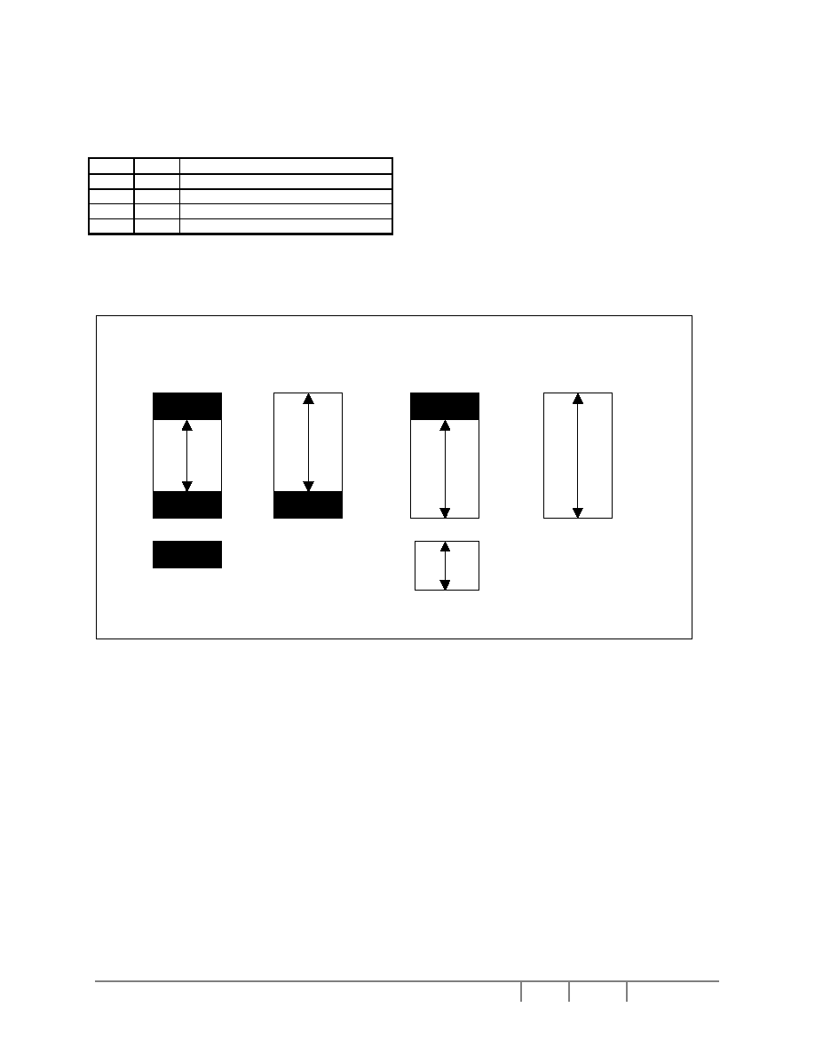
Solomon Systech
Sep 2003
P 36/61 Rev 1.00
SSD1770
Center Screen
Bottom Screen
Top Screen
Whole Screen Scroll
: Fixed Area
: Scroll Area
Part IV
Specify the area scroll type. Altogether there are four types of area scroll. Please refer to Table 11 for
detail.
P41
P40
Types of Area Scroll
0 0 Center
Screen
Scroll
0 1 Top
Screen
Scroll
1 0 Bottom
Screen
Scroll
1 1 Whole
Screen
Scroll
Table 11 - Area scrolling selection modes
Figure 11 - Area scrolling selection modes
The area scroll function is executed by prompt in the set area scroll command following by changing the
start block address by the set scroll start command. Figure 11 illustrates the operation model of the
scrolling function.

SSD1770
Rev 1.00 P 37/61 Sep 2003
Solomon Systech
Example: In the Center screen scroll of 1/64 duty (display range: 64 lines = 16 blocks)
Description
Command
Data
-
Set
Area
Scroll
AAH
-
8 lines (block 0 & block 1) are specified for the top fixed area
-
The Top Block Address = Number of the top fixed area
= 8 / 4
02H
-
8 lines (block 18 & block 19) are specified for the bottom fixed area
-
The Specified Bottom Block Address
= Bottom Block Address + Number of Background area
= 13 + ( 16 / 4 ) = 17 (11Hex)
11H
-
48 lines (block 2 to block 13) are specified the scroll area
-
Number of Specified Block
= Top fixed area + Scroll Area ≠ 1
= ( 8 / 4 ) + ( 48 / 4 ) ≠ 1 = 13 (0DHex)
0DH
-
16 lines (block 14 to block 17) are specified the background area
-
Set area scroll mode ≠ Center screen mode
00H
-
Set Scroll start (Scroll range form 02H ~ 11H)
ABH
02H
Figure 12 - GDDRAM updates for area scrolling
13
14
17
18
19
0
1
2
LCD panel
16 blocks
= 64 line
DDRAM:
Fixed area
Display area
Scroll area
Background area

Solomon Systech
Sep 2003
P 38/61 Rev 1.00
SSD1770
Figure 13 ≠ Example of Specified Center Scroll Mode
104 RGB X 64 lines Panel
104 RGB X 80 Line GDDRAM Content
Top Fix Area
Scroll Area
Background
Area
Bottom
Fix Area
COM0
COM63
COM0
COM63
COM0
COM63
COM0
COM63
Block
0
1
2
3
:
:
:
12
13
18
19
0
1
3
4
:
:
:
13
14
18
19
0
1
4
5
:
:
:
14
15
18
19
0
1
8
9
:
:
:
2
3
18
19
Scroll Start
= 2
Scroll Start
= 3
Scroll Start
= 4
Scroll Start
= 8
Example Program of Specified Center Scroll mode.
Void center_scroll(void)
{
//Set 1/64 Duty
Comm_out (0xCA);
Data_out (0x00);
Data_out (0x0F);
Data_out(0x00);
//Set Area Scroll
Comm_out(0xAA);
Data_out(0x02);
// Top Block Address
Data_out(0x11);
// Specified Bottom Block Address
Data_out(0x0D);
//Number of Specified Block
Data_out(0x00);
//Center Screen Mode
//Set Scroll Start
for (I=0x02; I<=0x11; I++)
{
Comm_out(0xAB); //set scroll start
Data_out(I);
Delay (200); //delay 200ms
}
}

SSD1770
Rev 1.00 P 39/61 Sep 2003
Solomon Systech
con
out
V
R
R
V
*
1
1
2
+
=
ref
con
V
V
*
210
63
1
-
-
=
9.8 Set Scroll Start
This command specifies the starting block address of the area scrolling and then executes the area scroll
by changing the start block address dynamically. Start block < End block must be maintained. Please be
noted that the set scroll start command should be executed after the set area scroll command.
9.9 Set Power Control Register
This command turns on/off the various power circuits associated with the chip. There are three power
sub-circuits (reference voltage generator, internal regulator and voltage follower) could be turned on/off by
this command. In addition, the configuration of the internal primary booster (3X/4X/5X/6X) can be
selected by this command.
9.10 Set Contrast Level & Internal Regulator Ratio
This command adjusts the contrast of the LCD panel by changing the LCD driving voltage, V
OUT
, provided
by the On-Chip power circuits. V
OUT
is set with 64 steps (6-bit) in the contrast control register by a set of
compound commands. Please refer to the Figure 14 for the contrast control process flow diagram.
Figure 14 - Contrast Control Flow Set Segment Re-map
This command also sets the feedback gain of the internal regulator. There are altogether 8 internal
regulator gains, which are used for the adjustment of V
OUT
level. This command is to enable any one of
the eight internal resistor (IRS) settings for different regulator gains when using internal regulator resistor
network. The Contrast Control Voltage Range curves is referred to the following formula:
Remarks: TC = -0.25%/
o
C
Changes
Complete?
No
Yes
Set Contrast Control Register
Contrast Level Data
where
,
V
Vref
7
.
1
=
Solomon Systech
Sep 2003
P 40/61 Rev 1.00
SSD1770
Contrast Curve
-
2
4
6
8
10
12
14
16
18
0
10
20
30
40
50
60
70
Contrast[0~63]
Vout[V]
IR0
IR1
IR2
IR3
IR4
IR5
IR6
IR7
Figure 15 - Contrast Control Voltage Range Curve (V
DD
=2.7V; V
CI
=3V; Booster level = 6X; TC = -0.25%/
o
C)
Note: The Maximum operation voltage of V
OUT
is 12.5V with panel load.
9.11 Set Increment/Decrement of the contrast set
This command can increase the contrast step by +1 and decrease the contrast set by ≠1. It is the most
convenient way to change the contrast of the display by programming.
9.12 Set Normal/Inverse Display
This command turns the display to be either normal or inverse. In normal display mode, a RAM data of 1
indicates an illumination on the corresponding pixel in the normal white panel. In inverse display mode, a
RAM data of 0 will turn on the pixel.
It should be noted that the icon line is not affected. The icon line is
not inversed by this command.
Example:
For a normal White display panel (Set Normal Display: A6Hex):
RAM Content
R G B
Color
F F F White
0 0 0 Black
F 0 0 Red
0 F 0 Green
0 0 F Blue
For a normal Black display panel (Set Normal Display: A7Hex):
RAM Content
R G B
Color
F F F White
0 0 0 Black
F 0 0 Red
0 F 0 Green
0 0 F Blue
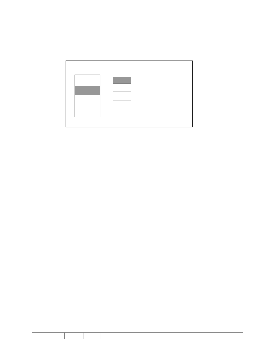
SSD1770
Rev 1.00 P 41/61 Sep 2003
Solomon Systech
:
Display area
(Partial Display Area)
: Non-display area
9.13 Enter Partial Display
This command and the following parameters specify the display area of the partial display mode. The
following figure shows the display and non-display area when the partial display mode is executed.
Figure 16 - Partial display mode
9.14 Exit Partial Display
This command exits the partial display mode.
9.15 Set Display On/Off
This command is used to turn the display on or off. When display off is issued with entire display is on,
power save mode will be entered.
9.16 Enter/Exit sleep mode
This command enter/exit the sleep mode.
9.17 Enable/Disable the internal oscillator
This command enables or disables the internal oscillator. The internal oscillator is turned off after
hardware or software reset.
9.18 Set Temperature compensation coefficient
This command sets the average temperature gradients. Four sets of average temperature gradients can
be selected. Please refer to the command table for detail description of the average temperature
gradients. The default value of the temperature gradient is ≠0.2 %/
0
C
9.19 NOP
A command causing the chip takes No Operation.
9.20 Write display data mode
This command is used to execute the write display data mode. The display data byte is directly written to
the GDDRAM. Please be noted that the
D/ C
signal should be set to high during the display data is written
to the GDDRAM.

Solomon Systech
Sep 2003
P 42/61 Rev 1.00
SSD1770
9.21 Read display data mode
This command is used to execute the read display data mode. The display data byte is directly red from
the GDDRAM. Please be noted that the
D/ C
signal should be set to high during the display data is read
from to the GDDRAM.
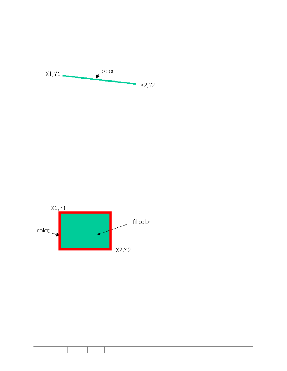
SSD1770
Rev 1.00 P 43/61 Sep 2003
Solomon Systech
Graphic Command
9.22 Draw Line
Given the starting point (X1, Y1) and the ending point (X2, Y2), a line will be drawn with the color
specified.
The following example illustrates the line drawing procedure.
1. Enter the "draw line mode" by execute the command 83H
2. Set the starting X-coordinates, X1. E.g., 00H.
3. Set the starting Y-coordinates, Y1. E.g., 00H.
4. Set the finishing X-coordinates, X2. E.g., 01H
5. Set the finishing Y-coordinates, Y2. E.g., 01H
6. Set the color to RGB = (0,1,0) e.g., 0FH following by 00H
Result: A color line will be drawn between coordinates (0,0) and (1,1)
Remarks: X1
103; X2
103; Y1
79; Y2 < 79
9.23 Fill Enable/Disable
This command allows the fill color option to be enabled or disabled. This command is applicable to the
Draw Rectangle feature. When the selection bit is "0", the fill color option is disabled. When the selection
bit is "1", the fill color option is enabled.
9.24 Draw rectangle
Given the starting point (X1, Y1) and the ending point (X2, Y2), specify the width and height of a rectangle
that will be drawn with the color specified. Remarks: If fill color option is disabled, the enclosed area will
not be filled.
The following example illustrates the rectangle drawing procedure.
1. Enter the "draw rectangle mode" by execute the command 8AH
2. Set the starting X-coordinates, X1. E.g., 00H.
3. Set the starting Y-coordinates, Y1. E.g., 00H.
4. Set the finishing X-coordinates, X2. E.g., 02H
5. Set the finishing Y-coordinates, Y2. E.g., 02H
6. Set the color to RGB = (1,0,0) e.g., F0H following by 00H
7. Set the filled color to RGB = (0,1,0) e.g., 0FH following by 00H
Result: A filled color square will be drawn with the coordinates of the top left hand corner at (0,0) and the
coordinates of the bottom right hand corner at (2,2)
Remarks: X1
X2; Y1
Y2; X2
103; Y2
79
Solomon Systech
Sep 2003
P 44/61 Rev 1.00
SSD1770
9.25 Copy
Copy the rectangular region defined by the starting point (X1, Y1) and the ending point (X2, Y2) to
location (X3, Y3). There are two possible results with the command copy executed depending on the
setting of the start point coordinates and end point coordinates.
The following example illustrates the copy procedure.
Case 1 ≠ The overlap region will superimpose.
1. Enter the "copy mode" by execute the command 84H
2. Set the starting X-coordinates, X1. E.g., 00H.
3. Set the starting Y-coordinates, Y1. E.g., 00H.
4. Set the finishing X-coordinates, X2. E.g., 02H
5. Set the finishing Y-coordinates, Y2. E.g., 02H
6. Set the New X-coordinates, X3. E.g., 01H
7. Set the New Y-coordinates, Y3. E.g., 01H
X1,Y1
X3,Y3
X2+X3,
Y2+Y3
X1,Y1
X2,Y2

SSD1770
Rev 1.00 P 45/61 Sep 2003
Solomon Systech
Case 2 ≠ The original GDDRAM content remains unchanged
1. Enter the "copy mode" by execute the command 84H
2. Set the starting X-coordinates, X1. E.g., 00H.
3. Set the starting Y-coordinates, Y1. E.g., 00H.
4. Set the finishing X-coordinates, X2. E.g., 01H
5. Set the finishing Y-coordinates, Y2. E.g., 01H
6. Set the New X-coordinates, X3. E.g., 09H
7. Set the New Y-coordinates, Y3. E.g., 09H
Remarks: X1
X2; Y1
Y2 ; X2
103; Y2
79
9.26 Dim Window
This command will dim the window area specify by starting point (X1, Y1) and the ending point (X2, Y2).
After the execution of this command, the selected window area will be dimmed by 75% white. Additional
execution of this command over the same window area will not change the data content.
Remarks: X1
X2; Y1
Y2; X2
103; Y2
79
9.27 Clear Window
This command sets the window area specify by starting point (X1, Y1) and the ending point (X2, Y2) to
clear the window display. The GDDRAM content of the window will be set to zero.
Remarks: X1
X2; Y1
Y2; X2
103; Y2
79
X1,Y1
X3,Y3
X2+X3,
Y2+Y3
X2,Y2

Solomon Systech
Sep 2003
P 46/61 Rev 1.00
SSD1770
Extended Command
9.28 Set biasing ratio
This command selects a suitable bias ratio (1/4 to 1/8) required for driving the particular LCD panel in
use.
9.29 Set Frame Frequency
This command specifies the frame frequency so as to minimize the flickering due to the ac main
frequency. The frequency is set to 78Hz after POR.
9.30 Set N-line inversion
Number of line inversion is set by this command for reducing crosstalk noise. 2 to 32-line inversion
operations could be selected. At POR, this operation is set to 0110b (7 lines). It should be noted that the
total number of mux (including the icon line) should NOT be a multiple of the inversion number (n). Or
else, some lines will not change their polarity during frame change.
9.31 Enable/disable icon
This command enable/disable the Icon display.
9.32 Select PWM/FRC
This command set the Pulse Width Modulation, Frame Rate Control or mix of FWM & FRC.
9.33 OTP setting and programming
OTP (One Time Programming) is a method to adjust V
OUT
. In order to eliminate the variations of LCD
module in terms of contrast level, OTP can be used to fine-tune the contrast of every LCD modules.
Each OTP bit can be programmed to `1' once.
OTP setting and programming should include two major steps. Find the OTP offset and OTP
programming as following,
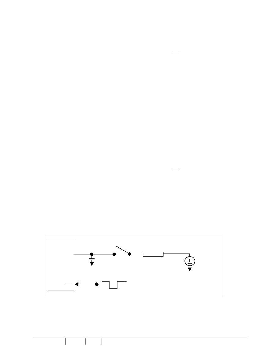
SSD1770
Rev 1.00 P 47/61 Sep 2003
Solomon Systech
Step 1. Find OTP offset
(1) Hardware Reset (sending an active low reset pulse to
RES pin)
(2) Send original initialization routines
(3) Set and display any test patterns
(4) Adjust the contrast value (C:0x81, D:0x00~0x3F, D: 0x00 ~ 0x07) until there is the best
visual contrast
(5) OTP setting steps = Contrast value of the best visual contrast - Contrast value of original
initialization
Example 1:
Contrast value of original initialization = 0x20
Contrast value of the best original initialization = 0x24
OTP offset value = 0x24 - 0x20 = +4
OTP setting command should be (C: 0xF6, D: 0x12, D: 0x0A)
Example 2:
Contrast value of original initialization = 0x20
Contrast value of the best original initialization = 0x1B
OTP setting = 0x1B - 0x20 = -6
OTP setting command should be (C:0xF6, D: 0x1D, D: 0x0A)
Step 2. OTP programming
(6) Hardware Reset (sending an active low reset pulse to
RES pin)
(7) Enable Oscillator (C: 0xD1) and Exit Sleep Mode (C: 0x94)
(8) Connect an external V
OUT
(see diagram below)
(9) Send OTP setting commands that we find in step 1 (C: 0xF6, D: 0x10~0x1F, D: 0x0A)
(10) Send OTP programming command (C: 0xF8)
(11) Wait at least 2 seconds
(12) Hardware Reset
(13) Verify the result by repeating step 1. (2) ≠ (3)
Figure 17 ≠ OTP programming circuitry
R
+
-
SSD1770
V
OUT
RES
14.5-15.5V
Note: R = 1K ~ 10k ohm
C = 1u ~ 4.7u F
C
(8)
(1) & (6) & (12)
GND
GND

Solomon Systech
Sep 2003
P 48/61 Rev 1.00
SSD1770
Figure 18 ≠ Flow chart of OTP programming Procedure
Start
OTP setting steps =
Adjusted contrast
value ≠ Original
contrast value
Connect an external
voltage (14.5~15.5V) on
V
OUT
pins
i) Send original initialization
routines
ii) Set and display any test
patterns
iii) Inspect the contrast
i) Hardware reset
ii) Enable oscillator
END
Yes
No
Adjust the
contrast level
to the best
visual level
Accept the
contrast level
on panel?
i) Send OTP setting commands
ii) Send OTP programming
command
iii) Wait > 2 sec
iv) Hardware reset
i) Hardware reset
ii) Send original initialization
routines
iii) Set and display any test
patterns
Step 1
Step 2

SSD1770
Rev 1.00 P 49/61 Sep 2003
Solomon Systech
OTP Example program
Find the OTP offset:
1.
Hardware reset by sending an active low reset pulse to
RES
pin
2. COMMAND(0XD1); \\Enable
oscillator;
COMMAND(0X94);
\\ exit sleep mode;
3.
COMMAND(0X20);
\\ turn on the reference voltage generator, internal regulator and voltage follower; Select booster level.
DATA(0X0B);
4.
COMMAND(0XCA)
\\ Set Duty ratio
DATA(0X10)
\\ 68Mux ([68 / 4] ≠1 = 16(decimal) / 10(Hex))
COMMAND(0XF7)
\\ Set PWM/FRC
DATA(0X28)
\\ pure PWM
DATA(0X2C)
DATA(0X05)
COMMAND(0XFB)
\\ Set Biasing ratio
DATA(0X3)
\\ 1/7
5.
COMMAND(0X81)
\\Set target gain and contrast.
DATA(0X14)
\\ contrast = 20
DATA(0X05)
\\ IR5 => gain = 7.16
6.
\\ Set target display contents
COMMAND(0X15)
\\ set column address
DATA(0x00)
\\ set start column address at 0
DATA(0X67)
\\ set end column address at 103
COMMAND(0X75)
\\ set page address
DATA(0X00)
\\ set start page address at 0
DATA(0X43)
\\ set end page address at 67
COMMAND(0X5C)
\\ write target content to GDDRAM
DATA(...)
COMMAND(0xAF) \\
display
on
7.
OTP offset calculation... target OTP offset value is +6
OTP programming:
8.
Hardware reset by sending an active low reset pulse to
RES
pin
9. COMMAND(0XD1) \\
Enable
Oscillator
10. COMMAND(0x94)
\\ Exit Sleep Mode
11. Connect a external V
OUT
(14.5V~15.5V)
12. COMMAND(0XF6)
\\ Set OTP offset value to +6 (0011)
DATA(0X13)
\\ 0001 X
3
X
2
X
1
X
0
, where X
3
X
2
X
1
X
0
is the OTP offset value
DATA(0x0A)
13. COMMAND(0XF8)
\\ Send the OTP programming command.
14. Wait at least 2 seconds for programming wait time.
Verify the result:
15. After OTP programming, procedure 2 to 5 are repeated for inspection of the contrast on the panel.

Solomon Systech
Sep 2003
P 50/61 Rev 1.00
SSD1770
Read Status Command
9.34 Status register read
This command will output the status of the device. Before sending the " status register read" command,
the command "read display data mode" should be sent to the device. The following parameters can be
monitored by the status read register.
1. Various area scroll mode
2. Column scan direction
3. Page scan direction
4. Display
ON/OFF
5. Sleep mode ON/OFF
6. Display
Normal/Inverse
7. Partial display mode ON/OFF

SSD1770
Rev 1.00 P 51/61 Sep 2003
Solomon Systech
10 MAXIMUM RATINGS
Table 12 - Maximum Ratings (Voltage Referenced to V
SS
)
Symbol Parameter
Value
Unit
V
DD
-0.3 to +4.0
V
V
OUT
Supply Voltage
-0.3 to 15
V
V
CI
Input
Voltage
V
SS
-0.3 to
4.0
V
I
Current Drain Per Pin Excluding V
DD
and
V
SS
25 mA
T
A
Operating Temperature
-40 to +85
o
C
T
stg
Storage Temperature
-65 to +150
o
C
Ron Input
Resistance
1000
ohm
Maximum ratings are those values beyond which damages to the device may occur. Functional operation should be restricted to the limits in the
Electrical Characteristics tables or Pin Description section
This device contains circuitry to protect the inputs against damage due to high static voltages or electric fields; however, it is advised that normal
precautions to be taken to avoid application of any voltage higher than maximum rated voltages to this high impedance circuit. For proper operation it
is recommended that V
CI
and V
OUT
be constrained to the range V
SS
< V
DD
V
CI
< V
OUT
. Reliability of operation is enhanced if unused input is
connected to an appropriate logic voltage level (e.g., either V
SS
or V
DD
). Unused outputs must be left open. This device may be light sensitive. Caution
should be taken to avoid exposure of this device to any light source during normal operation. This device is not radiation protected.
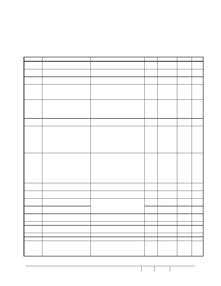
Solomon Systech
Sep 2003
P 52/61 Rev 1.00
SSD1770
11 DC CHARACTERISTICS
Table 13 - DC Characteristics (Unless otherwise specified, Voltage Referenced to V
SS
, V
DD
= 2.4 to 3.6V, T
A
= -40
to 85
∞C)
Symbol Parameter
Test
Condition
Min Typ
Max Unit
V
DD
System power supply pins of
the logic block Range
Recommend Operating Voltage
Possible Operating Voltage
2.4 2.7
3.6 V
V
DDIO
System power supply pins of
the logic block Range
Recommend Operating Voltage
Possible Operating Voltage
1.2 -
V
DD
V
V
CI
Booster Reference Supply
Voltage Range
Recommend Operating Voltage
Possible Operating Voltage
V
DD
-
3.6 V
I
AC
Access Mode Supply Current
Drain (V
DD
Pins)
V
DD
= 2.7V, Voltage Generator On,
5X DC-DC , Write accessing, Tcyc
=5MHz, Typ. Osc. Freq., Display
On, no panel attached.
- 400 1000
µA
I
DP2
Display Mode Supply Current
Drain (V
DD
Pins)
V
DD
= 2.7V, V
OUT
= 9.2V, Voltage
Generator On, 5X DC-DC
Converter Enabled, R/W(WR) Halt,
Typ. Osc. Freq., Display On, no
panel attached.
- 250 500
µA
I
SLEEP
Sleep Mode Supply Current
Drain (V
DD
Pins)
V
DD
= 2.7V, LCD Driving Waveform
Off, Oscillator Off, R/W(WR) halt.
- 2
5 µA
LCD Driving Voltage Generator
Output (V
OUT
Pin)
Display On, Voltage Generator
Enabled, DC-DC Converter
Enabled, Typ. Osc. Freq.,
Regulator Enabled, Divider
Enabled.
5
-
12.5
V
V
OUT
V
OUT
Converter Efficiency
6X boost, no panel loading
93
99
-
%
V
REF
Internal Reference Voltage (T =
25
o
C)
Reference Voltage (T = 25
o
C)
Reference Voltage (T = -20
o
C)
Reference Voltage (T = 70
o
C)
TC0 = -0.10%/
o
C
TC1 = -0.15%/
o
C
TC2 = -0.20%/
o
C (POR)
TC3 = -0.25%/
o
C
TC3 = -0.25%/
o
C
TC3 = -0.25%/
o
C
TC3 = -0.25%/
o
C
1.62
1.65
1.60
1.65
1.65
1.83
1.46
1.7
1.67
1.65
1.70
1.70
1.89
1.51
1.72
1.75
1.70
1.75
1.75
1.95
1.56
V
V
V
V
V
V
V
V
OH1
Logic High Output Voltage
Iout=-100 A
0.9
* V
DDIO
- V
DDIO
V
V
OL1
Logic Low Output Voltage
Iout=100 A
0
-
0.1
*V
DDIO
V
V
IH1
Logic High Input voltage
0.8*
V
DDIO
- V
DDIO
V
V
IL1
Logic Low Input voltage
0 -
0.2*
V
DDIO
V
I
OH
Logic High Output Current
Source
V
OUT
= V
DD
-0.4V 50
-
-
µA
I
OL
Logic Low Output Current Drain V
OUT
= 0.4V
-
-
-50
µA
I
OZ
Logic Output Tri-state Current
Drain Source
-1
-
1
µA
I
IL
/I
IH
Logic Input Current
-1
-
1
µA
C
IN
Logic Pins Input Capacitance
-
5
7.5
pF
V
OUT
Variation of V
OUT
Output (V
DD
is
fixed)
Regulator Enabled, Internal
Contrast Control Enabled, Set
Contrast Control Register = 0
-2 0
2 %

SSD1770
Rev 1.00 P 53/61 Sep 2003
Solomon Systech
Symbol Parameter
Test
Condition
Min Typ
Max Unit
TC0
Average Temperature Gradient
Flat Temperature Coefficient
0 -0.10 -0.12
%/
o
C
TC1
Temperature Coefficient 1
-0.12
-0.15
-0.17
%/
o
C
TC2
Temperature Coefficient 2
(POR)
-0.17 -0.20
-0.22 %/
o
C
TC3
Temperature Coefficient 3
Voltage Regulator Enabled
-0.22 -0.25
-0.27 %/
o
C
The formula for the temperature coefficient is:
%
100
x
C
25
at
V
1
x
C
0
C
50
C
0
at
V
C
50
at
V
(%)
TC
o
ref
o
o
o
ref
o
ref
-
-
=
12 AC CHARACTERISTICS
Table 14 - AC Characteristics (Unless otherwise specified, Voltage Referenced to V
SS
, V
DD
= 2.7V, T
A
= 25
o
C)
Symbol Parameter
Test
Condition
Min Typ Max Unit
Fosc
Oscillation Frequency of Display
Timing Generator for:
80 MUX Mode or 68 MUX mode
Internal Oscillator Enabled (default),
V
DD
= 2.7V
Remark: -0.2%/∞C (POR)
465.12
477.36
489.6
kHz
F
FRM
Frame Frequency for:
80 MUX Mode
Frame Frequency for:
68 MUX Mode
a. 104 RGB x 80 Graphic Display
Mode, Display ON, Internal
Oscillator Enabled
b. 104 RGB x 68 Graphic Display
Mode, Display ON, Internal
Oscillator Disabled, External clock
with freq., Fext, feeding to CL pin.
62.7
74.1
66
78
69.3
81.9
Hz
Hz
Remarks:
Fext stands for the frequency value of external clock feeding to the CL pin
Fosc stands for the frequency value of internal oscillator

Solomon Systech
Sep 2003
P 54/61 Rev 1.00
SSD1770
Table 15 ≠ Parallel Timing Characteristics (T
A
= -40 to 85
∞C, V
DD
= 2.4V to 3.6V)
Symbol Parameter
Min Typ Max Unit
t
cycle
Clock Cycle Time (write cycle)
166.6
-
-
ns
t
AS
Address Setup Time
15
-
-
ns
t
AH
Address Hold Time
10
-
-
ns
t
DSW
Data Setup Time
10
-
-
ns
t
DHW
Data Hold Time
20
-
-
ns
t
ACC
Data Access Time
15
-
200
ns
t
OH
Output Hold time
20
-
60
ns
Figure 19 ≠ Parallel 6800-series Interface Timing Characteristics (PS0 = H, PS1 = H)
t
cycle
D
0
~D
7
(WRITE)
D
0
~D
7
(READ)
CS
E
PW
CSH
t
R
t
F
t
DHW
t
OH
t
ACC
t
DHR
Valid Data
t
DSW
Valid Data
PW
CSL
W
/
R
t
AH
t
AS
C
/
D

SSD1770
Rev 1.00 P 55/61 Sep 2003
Solomon Systech
Table 16 ≠ Parallel Timing Characteristics (T
A
= -40 to 85
∞C, V
DD
= 2.4V to 3.6V)
Symbol Parameter
Min Typ Max Unit
t
cycle
Clock Cycle Time (write cycle)
166.6
-
-
ns
t
AS
Address Setup Time
15
-
-
ns
t
AH
Address Hold Time
10
-
-
ns
t
DSW
Data Setup Time
10
-
-
ns
t
DHW
Data Hold Time
20
-
-
ns
t
ACC
Data Access Time
15
-
170
ns
t
OH
Output Hold time
20
-
60
ns
Figure 20 ≠ Parallel 8080-series Interface Timing Characteristics (PS0 = H, PS1 = L)
PW
CSH
PW
CSL
t
DSW
t
DHW
t
OH
t
ACC
Valid Data
t
DHR
t
cycle
t
AH
t
AS
C
/
D
RD
CS
Valid Data
D
0
~D
7
(WRITE)
D
0
~D
7
(READ)
WR
t
R
t
F
PW
CSH
PW
CSL
t
AH
t
AS
C
/
D
CS
WR
t
R
t
F
RD
Write Cycle
Read Cycle
t
cycle

Solomon Systech
Sep 2003
P 56/61 Rev 1.00
SSD1770
Table 17 - Serial Timing Characteristics (T
A
= -40 to 85
∞C, V
DD
= 2.4V to 3.6V)
Symbol Parameter
Min Typ Max Unit
t
cycle
Clock Cycle Time
66.6
-
-
ns
f
CLK
Serial Clock Cycle Time
SPI Clock tolerance = +/- 2 ppm
- - 15
MHz
t
AS
Register select Setup Time
90
-
-
ns
t
AH
Register select Hold Time
20
-
-
ns
t
CSS
Chip Select Setup Time
10
-
-
ns
t
CSH
Chip Select Hold Time
30
-
-
ns
t
DSW
Write Data Setup Time
10
-
-
ns
t
OHW
Write Data Hold Time
10
-
-
ns
t
CLKL
Clock Low Time
15
-
-
ns
t
CLKH
Clock High Time
15
-
-
ns
Figure 21 - Serial Timing Characteristics (PS0 = L, PS1 =L)
t
AH
t
AS
C
/
D
Valid Data
t
DHW
t
CLKL
t
DSW
t
CLKH
t
cycle
t
CSS
t
CSH
t
F
t
R
SDA(D
7
)
CS
SCK(D
6
)
D7
SDA(D
7
)
CS
SCK(D
6
)
D6
D5
D4
D3
D2
D1
D0

SSD1770
Rev 1.00 P 57/61 Sep 2003
Solomon Systech
13 APPLICATION EXAMPLES
Figure 22 - Application Example I (4-wires SPI mode)
,where
V
DD
& V
CI
= 2.775V;
V
DDIO
= 2.775V;
C
1
= 1uF ~2uF;
C
2
= 2.2uF ~ 4.7uF.
Logic pin connections not specified above:
Pins connected to V
DD
: E; R/
W
; D
0
~D
5
;
Pins connected to V
SS
: PS0; PS1; RV
SS
; CV
SS
; MUX68/(
80
); VL
REF
;
Pin connected to V
OUT
: VH
REF
;
Pin connected to V
CI
: V
CIX2
;
CS RES
C
/
D
COL0 .....................................................................................................COL311
ROW79 ..........ROW40
ROW39 ................ICON
SE
G103-
B
SE
G103-
G
SE
G103-
R
SE
G102-
B
SE
G102-
G
SE
G102-
R
:
:
:
:
:
:
:
:
:
:
:
:
:
:
:
:
:
:
:
SE
G
1
-B
SE
G
1
-G
SE
G
1
-R
SE
G
0
-B
SE
G
0
-G
SE
G
0
-R
COM40
COM41
:
:
:
:
:
:
:
COM78
COM79
ICON
COM0
COM1
:
:
:
:
:
:
:
COM38
COM39
Output scan
command
[command: BBH,
Data:01H]
DISPLAY PANEL SIZE
104RGB X 80 + ICON LINE
SSD1770 IC (DIE FACE UP)
SCK SDA
C
1
C
2
V
DD
V
CI
V
SS
V
OUT
V
DDIO

Solomon Systech
Sep 2003
P 58/61 Rev 1.00
SSD1770
Figure 23 - Application Example II (6800 PPI mode)
,where
V
DD
& V
CI
= 2.775V;
V
DDIO
= 2.775V;
C
1
= 1uF ~ 2.2uF;
C
2
= 2.2uF ~ 4.7uF.
Logic pin connections not specified above:
Pins connected to V
DD
: PS0; PS1;
Pins connected to V
SS
: RV
SS
; CV
SS
; MUX68/(
80
); VL
REF
;
Pin connected to V
OUT
: VH
REF
;
Pin connected to V
CI
: V
CIX2
;
CS RES
C
/
D
D
0
...D
7
COL0 .....................................................................................................COL311
ROW79 ..........ROW40
ROW39 ................ICON
SE
G103-
B
SE
G103-
G
SE
G103-
R
SE
G102-
B
SE
G102-
G
SE
G102-
R
:
:
:
:
:
:
:
:
:
:
:
:
:
:
:
:
:
:
:
SE
G
1
-B
SE
G
1
-G
SE
G
1
-R
SE
G
0
-B
SE
G
0
-G
SE
G
0
-R
COM40
COM41
:
:
:
:
:
:
:
COM78
COM79
ICON
COM0
COM1
:
:
:
:
:
:
:
COM38
COM39
Output scan
command
[command: BBH,
Data:01H]
DISPLAY PANEL SIZE
104RGB X 80 + ICON LINE
SSD1770 IC (DIE FACE UP)
W
/
R
E
C
1
C
2
V
DD
V
CI
V
SS
V
OUT
V
DDIO

SSD1770
Rev 1.00 P 59/61 Sep 2003
Solomon Systech
Figure 24 ≠ Applications notes for V
DD
/V
DDIO
connection
MCU
SSD1770
/CS
/RES
D/C
R/W
E
D
0
~D
7
V
OUT
VH
REF
2.775V
2.775V
2.775V
V
DDIO
V
DD
V
CI
PS0
PS1
MCU
SSD1770
/CS
/RES
D/C
R/W
E
D
0
~D
7
V
OUT
VH
REF
2.4V
2.775V or
2.4V
2.4V
V
DDIO
V
DD
V
CI
PS0
PS1
2.775V
V
SS
CV
SS
RV
SS
VL
REF
V
SS
CV
SS
RV
SS
VL
REF
Normal Application
Low Voltage MCU

Solomon Systech
Sep 2003
P 60/61 Rev 1.00
SSD1770
14 SSD1770Z DIE TRAY DIMENSIONS
Spec mm
(mil)
W1
2
.
0
1
.
0
0
.
76
+
-
(2992)
W2
2
.
0
1
.
0
0
.
68
+
-
(2677)
X1
4.0
± 0.1
(158)
Y1
1.40
± 0.1
(55)
X
17.85
± 0.1 (703)
Y
2.07
± 0.1
(82)
Z
0.73
± 0.1
(29)
N 54

SSD1770
Rev 1.00 P 61/61 Sep 2003
Solomon Systech
Solomon Systech reserves the right to make changes without further notice to any products herein. Solomon Systech makes no warranty,
representation or guarantee regarding the suitability of its products for any particular purpose, nor does Solomon Systech assume any liability arising
out of the application or use of any product or circuit, and specifically disclaims any and all liability, including without limitation consequential or
incidental damages. "Typical" parameters can and do vary in different applications. All operating parameters, including "Typicals" must be validated for
each customer application by customer's technical experts. Solomon Systech does not convey any license under its patent rights nor the rights of
others. Solomon Systech products are not designed, intended, or authorized for use as components in systems intended for surgical implant into the
body, or other applications intended to support or sustain life, or for any other application in which the failure of the Solomon Systech product could
create a situation where personal injury or death may occur. Should Buyer purchase or use Solomon Systech products for any such unintended or
unauthorized application, Buyer shall indemnify and hold Solomon Systech and its offices, employees, subsidiaries, affiliates, and distributors harmless
against all claims, costs, damages, and expenses, and reasonable attorney fees arising out of, directly or indirectly, any claim of personal injury or
death associated with such unintended or unauthorized use, even if such claim alleges that Solomon Systech was negligent regarding the design or
manufacture of the part
http://www.solomon-systech.com