
i
TABLE OF CONTENTS
GENERAL DESCRIPTION ........................................................................................................................... 1
FEATURES ................................................................................................................................................... 1
ORDERING INFORMATION ........................................................................................................................ 2
BLOCK DIAGRAM ....................................................................................................................................... 3
PIN ARRANGEMENT OF SSD1801Z GOLD BUMP DIE............................................................................ 4
PIN ARRANGEMENT OF SSD1801AV BARE DIE..................................................................................... 7
PIN DESCRIPTIONS .................................................................................................................................... 9
FUNCTIONAL BLOCK DESCRIPTIONS................................................................................................... 12
VOLTAGE GENERATOR CIRCUIT ........................................................................................................... 21
FRAME FREQUENCY................................................................................................................................ 22
COMMAND TABLE .................................................................................................................................... 23
COMMAND DESCRIPTIONS ..................................................................................................................... 25
MAXIMUM RATINGS ................................................................................................................................. 30
DC CHARACTERISTICS............................................................................................................................ 31
AC CHARACTERISTICS............................................................................................................................ 33
APPLICATION EXAMPLES ....................................................................................................................... 37


SOLOMON SYSTECH
SEMICONDUCTOR TECHNICAL DATA
This document contains information on a new product under definition stage. Solomon Systech Limited reserves
the right to change or discontinue this product without notice.
http://www.solomon-systech.com
SSD1801
Rev 1.1
P 1
Jan 2003
Copyright
2003 Solomon Systech Limited
SSD1801
Advance Information
LCD Segment / Common Driver with Controller
for Character Display System
CMOS
GENERAL DESCRIPTION
SSD1801 is a single-chip CMOS LCD driver with controller for liquid crystal dot-matrix character display
system. It consists of 105 high voltage driving output pins for driving 80 Segments, 24 Commons and 1 icon
driving-Common. It can display 2 or 3 lines of 16 characters with 5x8 dots format. The double height character
mode and line vertical scroll functions are supported.
SSD1801 displays character directly from its internal 10,240 bits (256 characters x 5 x 8 dots) Character
Generator ROM (CGROM). All the character codes are stored in the 512 bits (16 character x 4 lines) Data
Display RAM (DDRAM). User defined character can be loaded via 320 bits (8 characters x 5 x 8 dots) Character
Generator RAM (CGRAM). In addition, there is a 80 bits Icon RAM for Icon display. Data/ Commands are sent
from general MCU through a software selectable 6800-/8080-series compatible 4/ 8-bit Parallel Interface or Serial
Peripheral Interface.
SSD1801 embeds a DC-DC Converter, Voltage Regulator, Voltage divider and RC oscillator which reduce the
number of external components. With the special design on minimizing power consumption and die size,
SSD1801 is suitable for portable battery-driven applications requiring a long operation period and a compact
size.
FEATURES
Single Supply Operation, 2.4V - 3.6V
Maximum 5.8V LCD Driving Output Voltage
Low Current Sleep Mode
On-Chip 2x/3x DC-DC Converter/ External Power Supply
On-Chip RC Oscillator/ External Clock
On-Chip Voltage Regulator
On-Chip Voltage Divider with programmable bias ratio (1/4, 1/5)
32 Level Internal Contrast Control/ External Contrast Control
2 or 3 lines x 16 characters with 5x8 dots format display and 80 icons
Double Height Character Mode, Blink Mode, Cursor Display and Line Vertical Scroll Functions
Row remapping and column remapping (4-type LCD application available)
8/4-bit 6800-series Parallel Interface, 8/4-bit 8080-series Parallel Interface and Serial Peripheral Interface
256 Build in characters and 8 user defined characters
On-Chip Memories
Character Generator ROM (CGROM): 10240 bits (256 characters x 5 x 8 dots)
Character Generator RAM (CGRAM): 320 bits (8 characters x 5 x 8 dots)
Display Data RAM (DDRAM): 512 bits (16 characters x 4 lines)
Segment Icon RAM (ICONRAM): 80 bits (80 icons)
Available in Gold Bump Die and Bare Die

Solomon Systech
Jan 2003
P 2/41
Rev 1.1
SSD1801
ORDERING INFORMATION
Table 1 - Ordering Information
Ordering Part
Number
Package Form
SSD1801Z
Gold Bump Die
SSD1801AV Bare
Die

SSD1801
Rev 1.1
P 3/41
Jan 2003
Solomon Systech
BLOCK DIAGRAM
Figure 1 � Block Diagram of SSD1801

Solomon Systech
Jan 2003
P 4/41
Rev 1.1
SSD1801
PIN ARRANGEMENT OF SSD1801Z GOLD BUMP DIE
Alignment Keys
Figure 2 � SSD1801Z Pin Arrangement
Die Size:
6170um x 1480um (include scribe line)
6070um x 1380um (exclude scribe line)
Die Thickness:
670 +/-25um
Bump Size
Minimum Pitch
PAD: 1-63
52.15 x 60.2 um
76.3um
PAD: 65-79,
164-178 74.9 x 42 um
63.7um
PAD: 81-162
42 x 74.9 um
63.7um
PAD: 64,80,163,179
52.15 X 52.15 um
Bump Height: Nominal
18um
Note:
1. The die faces up in the diagram.
2. Coordinates are reference to the center of the chip.
3. Unit of coordinates and size of all alignment keys are in um.
4. All alignment keys do not contain gold bump.
(-2835, -598.5)
X
37.6
�m
8.75
�m
(2835, -598.5)
X
37.6
�m
8.75
�m
26.3
�
m 26.3
�
m 26.3
�
m
X
Center (-2940.9, 480.0)
26.3
�m 26.3 �m 26.3 �m
26.3
�
m
52.5
�
m
X
Center (2940.9, 480.0)
26.3
�m 26.3 �m 26.3 �m
13.1
�
m
61.3
�
m
61.3
�m
8.
8
�
M
13.1
�
m
Center (-2101.9, 169.6)
X

SSD1801
Rev 1.1
P 5/41
Jan 2003
Solomon Systech
Table 2 � SSD1801Z Gold Bump Die Pad Coordinates
PAD#
NAME
X Y
PAD#
NAME
X Y
1
D/ C
-2401.53 -600.78 41
C1N
684.78 -600.78
2 DVSS
-2325.23
-600.78 42 C1N 761.08
-600.78
3
R/
W ( WR ) -2248.93 -600.78 43
C1P
837.38 -600.78
4 DVDD
-2172.63
-600.78 44 C1P 913.68
-600.78
5
E( RD )
-2096.33 -600.78 45
VEXT 989.98 -600.78
6
CS
-2020.03 -600.78 46
DVSS 1080.63 -600.78
7 D7
-1943.73
-600.78
47
AVSS
1156.93
-600.78
8 D6
-1867.43
-600.78
48
DVSS
1233.23
-600.78
9
D5 -1791.13
-600.78 49 REF 1309.53
-600.78
10 D4
-1714.83
-600.78
50 DIRS
1385.83
-600.78
11 D3
-1638.53
-600.78
51
DVDD
1462.13
-600.78
12 D2
-1562.23
-600.78
52
AVDD
1538.43
-600.78
13 D1
-1485.93
-600.78
53
DVDD
1614.73
-600.78
14 D0
-1409.63
-600.78
54 CLK
1691.03
-600.78
15 DVDD
-1333.33
-600.6 55 VSS 1767.33
-600.78
16 AVDD
-1257.03
-600.6 56 P / S
1843.63 -600.78
17 DVDD
-1180.73
-600.6 57 DVDD
1919.93
-600.78
18 DVSS
-1104.43
-600.78 58 DL 1996.23
-600.78
19 AVSS
-1028.13
-600.6 59 DVSS
2072.53
-600.78
20 DVSS -951.83 -600.6 60
C68/( 80 )
2148.83 -600.78
21 VL2 -861.18
-600.6 61 DVDD
2225.13
-600.78
22 VL2 -784.88
-600.6 62 RES
2301.43 -600.78
23 VL3 -708.58
-600.6 63 TEST
2377.73
-600.78
24 VL3 -632.28
-600.78
64 NC 2939.3
-600.78
25 VL4 -555.98
-600.78
65 NC 2939.3
-520.1
26 VL4 -479.68
-600.78
66
COMI0
2939.3
-456.4
27 VL5 -403.38
-600.78
67
COM
0
2939.3
-392.7
28 VL5 -327.08
-600.78
68
COM
1
2939.3 -329
29 VL6 -246.05
-600.78
69
COM
2
2939.3
-265.3
30 VL6 -169.75
-600.78
70
COM
3
2939.3
-201.6
31 VL6 -93.45
-600.78
71
COM
4
2939.3
-137.9
32 VL6 -17.15 -600.78 72 COM
5 2939.3 -74.2
33 VF 64.75 -600.78 73 COM
6 2939.3 -10.5
34 VF 141.05
-600.78
74
COM
7
2939.3
53.2
35 VOUT 222.25 -600.78 75 COM16 2939.3 116.90
36 VOUT 298.55 -600.78 76 COM17 2939.3 180.6
37 C2N 379.58 -600.78 77 COM18 2939.3 244.3
38 C2N 455.88 -600.78 78 COM19 2939.3 308.0
39 C2P 532.18
-600.78
79 NC 2939.3
371.7
40 C2P 608.48
-600.78
80 NC 2939.3
593.43
Solomon Systech
Jan 2003
P 6/41
Rev 1.1
SSD1801
PAD#
NAME X
Y PAD#
NAME X
Y
81 NC
2579.85
593.43
131
SEG49
-605.15
593.43
82 SEG0
2516.15
593.43 132 SEG50
-668.85
593.43
83 SEG1
2452.45
593.43 133 SEG51
-732.55
593.43
84 SEG2
2388.75
593.43 134 SEG52
-796.25
593.43
85 SEG3
2325.05
593.43 135 SEG53
-859.95
593.43
86 SEG4
2261.35
593.43 136 SEG54
-923.65
593.43
87
SEG5
2197.65
593.43 137 SEG55
-987.35
593.43
88 SEG6
2133.95
593.43 138 SEG56
-1051.05
593.43
89 SEG7
2070.25
593.43 139 SEG57
-1114.75
593.43
90 SEG8
2006.55
593.43 140 SEG58
-1178.45
593.43
91 SEG9
1942.85
593.43 141 SEG59
-1242.15
593.43
92 SEG10
1879.15
593.43 142 SEG60
-1305.85
593.43
93 SEG11
1815.45
593.43 143 SEG61
-1369.55
593.43
94 SEG12
1751.75
593.43 144 SEG62
-1433.25
593.43
95 SEG13
1688.05
593.43 145 SEG63
-1496.95
593.43
96 SEG14
1624.35
593.43 146 SEG64
-1560.65
593.43
97 SEG15
1560.65
593.43 147 SEG65
-1624.35
593.43
98 SEG16
1496.95
593.43 148 SEG66
-1688.05
593.43
99 SEG17
1433.25
593.43 149 SEG67
-1751.75
593.43
100 SEG18 1369.55 593.43 150 SEG68 -1815.45 593.43
101 SEG19 1305.85 593.43 151 SEG69 -1879.15 593.43
102 SEG20 1242.15 593.43 152 SEG70 -1942.85 593.43
103 SEG21 1178.45 593.43 153 SEG71 -2006.55 593.43
104 SEG22 1114.75 593.43 154 SEG72 -2070.25 593.43
105 SEG23 1051.05 593.43 155 SEG73 -2133.95 593.43
106 SEG24 987.35 593.43 156 SEG74 -2197.65 593.43
107 SEG25 923.65 593.43 157 SEG75 -2261.35 593.43
108 SEG26 859.95 593.43 158 SEG76 -2325.05 593.43
109 SEG27 796.25 593.43 159 SEG77 -2388.75 593.43
110 SEG28 732.55 593.43 160 SEG78 -2452.45 593.43
111 SEG29 668.85 593.43 161 SEG79 -2516.15 593.43
112 SEG30 605.15 593.43 162 NC -2579.85 593.43
113 SEG31 541.45 593.43 163 NC -2939.3 593.43
114 SEG32 477.75 593.43 164 NC -2939.3 371.7
115 SEG33 414.05 593.43 165 COMI1 -2939.3 308
116 SEG34 350.35 593.43 166 COM23 -2939.3 244.3
117 SEG35 286.65 593.43 167 COM22 -2939.3 180.6
118 SEG36 222.95 593.43 168 COM21 -2939.3 116.9
119 SEG37 159.25 593.43 169 COM20 -2939.3 53.2
120 SEG38 95.55 593.43 170 COM15 -2939.3 -10.5
121 SEG39 31.85 593.43 171 COM14 -2939.3 -74.2
122 SEG40 -31.85 593.43 172 COM13 -2939.3 -137.9
123 SEG41 -95.55 593.43 173 COM12 -2939.3 -201.6
124 SEG42 -159.25 593.43 174 COM11 -2939.3 -265.3
125 SEG43 -222.95 593.43 175 COM10 -2939.3 -329
126 SEG44 -286.65 593.43 176 COM9 -2939.3 -392.7
127 SEG45 -350.35 593.43 177 COM8 -2939.3 -456.4
128 SEG46 -414.05 593.43 178 NC -2939.3 -520.1
129 SEG47 -477.75 593.43 179 NC -2939.3 -600.78
130
SEG48
-541.45
593.43

SSD1801
Rev 1.1
P 7/41
Jan 2003
Solomon Systech
PIN ARRANGEMENT OF SSD1801AV BARE DIE
Figure 3 � SSD1801AV Pin Arrangement
Die Size:
6296um x 1845um +/- 36um (include scribe line)
Die Thickness:
670 +/-25um
Pad Metal Size:
88 x 88um
Pad Opening Size:
80 x 80um
Pad
number
Pad
metal
size
PADS: 1-9, 48-56, 72-80, 119-127
103um x111um
PADS: 57, 58, 70, 71, 128, 129, 141, 142
111um x103um
PADS:
10-47,
81-118
90um
x111um
PADS:
59-69,
130-140
111um
x90um
Note:
1. The die faces up in the diagram.
2. Coordinates are reference to the center of the chip.

Solomon Systech
Jan 2003
P 8/41
Rev 1.1
SSD1801
Table 3 - SSD1801AV Bare Die Pad Coordinates
PAD #
NAME
X
Y
PAD # NAME
X
Y
PAD #
NAME
X
Y
1
COM21 -2748.20 -772.71 51 COM3 2198.53 -772.71 101 SEG41 -145.08 772.98
2
COM20 -2638.13 -772.71 52 COM4 2308.60 -772.71 102 SEG42 -239.93 772.98
3
COM15 -2528.05 -772.71 53 COM5 2418.68 -772.71 103 SEG43 -334.78 772.98
4
COM14 -2417.98 -772.71 54 COM6 2528.75 -772.71 104 SEG44 -429.63 772.98
5
COM13 -2307.90 -772.71 55 COM7 2638.83 -772.71 105 SEG45 -524.48 772.98
6
COM12 -2197.83 -772.71 56 COM16
2748.90 -772.71 106 SEG46 -619.33 772.98
7
COM11 -2087.75 -772.71 57 COM17
2998.10 -687.75 107 SEG47 -714.18 772.98
8
COM10 -1977.68 -772.71 58 COM18
2998.10 -577.68 108 SEG48 -809.03 772.98
9
COM9 -1867.60 -772.71 59 COM19
2998.10 -467.60 109 SEG49 -903.88 772.98
10
COM8 -1757.53 -772.71 60 SEG0 2998.10 -372.75 110 SEG50 -998.73 772.98
11
D/ C
-1662.68 -772.71 61 SEG1 2998.10 -277.90 111 SEG51 -1093.58 772.98
12 R/W ( WR ) -1567.83 -772.71 62 SEG2 2998.10 -183.05 112 SEG52 -1188.43 772.98
13
E( RD )
-1472.98 -772.71 63 SEG3 2998.10 -88.20 113 SEG53 -1283.28 772.98
14
CS
-1378.13 -772.71 64 SEG4 2998.10
6.65 114 SEG54 -1378.13 772.98
15
D7
-1283.28 -772.71 65 SEG5 2998.10 101.50 115 SEG55 -1472.98 772.98
16
D6
-1187.73 -772.71 66 SEG6 2998.10 196.35 116 SEG56 -1567.83 772.98
17
D5
-1092.18 -772.71 67 SEG7 2998.10 291.20 117 SEG57 -1662.68 772.98
18
D4
-996.63 -772.71 68 SEG8 2998.10 386.05 118 SEG58 -1757.53 772.98
19
D3
-901.08 -772.71 69 SEG9 2998.10 480.90 119 SEG59 -1867.60 772.98
20
D2
-805.53 -772.71 70 SEG10 2998.10 590.98 120 SEG60 -1977.68 772.98
21
D1
-709.98 -772.71 71 SEG11 2998.10 701.05 121 SEG61 -2087.75 772.98
22 D0 -614.43
-772.71
72
SEG12
2742.43
772.98
122
SEG62
-2197.83
772.98
23
VL2
-519.58 -772.71 73 SEG13 2632.35 772.98 123 SEG63 -2307.90 772.98
24
VL3
-424.73 -772.71 74 SEG14 2522.28 772.98 124 SEG64 -2417.98 772.98
25
VL4
-329.88 -772.71 75 SEG15 2412.20 772.98 125 SEG65 -2528.05 772.98
26
VL5
-235.03 -772.71 76 SEG16 2302.13 772.98 126 SEG66 -2638.13 772.98
27
VL6
-140.18 -772.71 77 SEG17 2192.05 772.98 127 SEG67 -2748.20 772.98
28
VF
-45.33 -772.71 78 SEG18 2081.98 772.98 128 SEG68 -2998.10 -687.75
29
VOUT
49.53 -772.71 79 SEG19 1971.90 772.98 129 SEG69 -2998.10 -577.68
30
C2N
144.38 -772.71 80 SEG20 1861.83 772.98 130 SEG70 -2998.10 -467.60
31
C2P
239.23 -772.71 81 SEG21 1751.75 772.98 131 SEG71 -2998.10 -372.75
32
C1N
334.08 -772.71 82 SEG22 1657.08 772.98 132 SEG72 -2998.10 -277.90
33
C1P
428.93 -772.71 83 SEG23 1562.23 772.98 133 SEG73 -2998.10 -183.05
34
VEXT
523.78 -772.71 84 SEG24 1467.38 772.98 134 SEG74 -2998.10 -88.20
35
AVSS
618.63 -772.71 85 SEG25 1372.53 772.98 135 SEG75 -2998.10
6.65
36
DVSS
713.48 -772.71 86 SEG26 1277.68 772.98 136 SEG76 -2998.10 101.50
37
REF
808.33 -772.71 87 SEG27 1182.83 772.98 137 SEG77 -2998.10 196.35
38
DIRS
903.18 -772.71 88 SEG28 1087.98 772.98 138 SEG78 -2998.10 291.20
39
AVDD
998.03 -772.71 89 SEG29 993.13 772.98 139 SEG79 -2998.10 386.05
40
DVDD 1092.88 -772.71 90 SEG30 898.28 772.98 140 ICONS2 -2998.10 480.90
41
CLK
1187.73 -772.71 91 SEG31 803.43 772.98 141 COM23 -2998.10 590.98
42
P/ S
1282.58 -772.71 92 SEG32 708.58 772.98 142 COM22 -2998.10 701.05
43
DL 1377.43
-772.71
93
SEG33 613.73
772.98
44
C68/( 80 ) 1472.28
-772.71
94
SEG34 518.88
772.98
45
RES
1567.13
-772.71
95
SEG35 424.03
772.98
46 TEST 1661.98
-772.71
96
SEG36 329.18
772.98
47 ICONS1 1758.23
-772.71
97
SEG37 234.33
772.98
48 COM0 1868.30
-772.71
98
SEG38 139.48
772.98
49 COM1 1978.38
-772.71
99
SEG39 44.63
772.98
50 COM2 2088.45
-772.71
100
SEG40 -50.23
772.98

SSD1801
Rev 1.1
P 9/41
Jan 2003
Solomon Systech
PIN DESCRIPTIONS
D/ C
This pin is Data/ Command control pin. When the pin is pulled high, the data at D
7
-D
0
is treated as display data.
When the pin is pulled low, the data at D
7
-D
0
will be transferred to the command register.
R/
W
( WR )
This pin is microprocessor interface input. When interfacing to a 6800-series microprocessor, this pin will be used
as R/W signal input. Read mode will be carried out when this pin is pulled high and write mode when low.
When interfacing to a 8080-microprocessor, this pin will be the WR input. Data write operation is initiated when
this pin is pulled low and the chip is selected.
This pin must be fixed to high or low in serial mode.
DVDD & AVDD
Digital and Analog Power supply pin.
DVSS & AVSS
Ground.
E( RD )
This pin is microprocessor interface input. When interfacing to a 6800-series microprocessor, this pin will be used
as the enable signal, E. Read/ Write operation is initiated when this pin is pulled high and the chip is selected.
When interfacing to a 8080-microprocessor, this pin receives the RD signal. Data read operation is initiated when
this pin is pulled low and the chip is selected.
This pin must be fixed to high or low in serial mode.
CS
This pin is the chip select input.
D
7
-D
0
These pins are the 8-bit bi-directional data bus to be connected to the microprocessor in parallel interface mode.
In 8-bit bus mode, D
7
is the MSB while D
0
is the LSB. In 4-bit bus mode, it is needed to transfer 4-bit data (through
D
7
-D
4
) by two times. The high order bits (for 8-bit mode D
7
-D
4
) are written before the low order bits (for 8-bit mode
D
3
-D
0
) in write transaction and low order bits (8-bit mode D
3
-D
0
) are read before the high order bits (8-bit mode D
7
-
D
4
) in read transaction. The D
3
-D
0
pins must be fixed to high or low in 4-bit bus mode. After resets, SSD1801
considers first 4-bit data from MPU as the high order bits.
When serial mode is selected, D
7
is the serial data input (SDA) and D
6
is the serial clock input (SCK). D5-D0 must
be fixed to high or low in serial mode
V
L6
, V
L5
, V
L4
, V
L3
, V
L2
LCD driving voltages. They can be supplied externally or generated by the internal bias divider. They have the
following relationship:
V
L6
> V
L5
> V
L4
> V
L3
> V
L2
> V
ss
1:4 bias
1:5 bias (default)
VL5
3/4 * VL6
4/5 * VL6
VL4
2/4 * VL6
3/5 * VL6
VL3
2/4 * VL6
2/5 * VL6
VL2
1/4 * VL6
1/5 * VL6
VL6 is the most positive LCD driving voltage. It can be supplied externally or generated by the internal regulator. It is
recommended to add a capacitor between VL6 and Vss for external regulator.

Solomon Systech
Jan 2003
P 10/41 Rev 1.1
SSD1801
VF
This pin is the input of the built-in voltage regulator. When external resistor network is selected to generate the
LCD driving level, V
L6
, two external resistors, R
1
and R
2
, are connected between AV
SS
and V
F
, and V
F
and V
L6
,
respectively (see application circuit)
VOUT
Regulated DC/DC voltage converter output. External capacitor is connected to AVDD for internal regulated DC-
DC converter and divider mode only.
VEXT
This is an input pin to provide an external voltage reference for the internal voltage regulator. It is selected by REF
signal pin. Leave this pin open (NC) if internal voltage regulator is used.
REF
This pin is to select the input voltage of internal voltage regulator. When this pin is pulled low, the internal voltage
reference V
REF
is used. When this pin is pulled high, external voltage reference (V
EXT
) is selected.
DIRS
This pin controls the direction of Segment.
When DIRS = Low
SEG0 -> SEG2 -> ..... -> SEG78 -> SEG79
When DIRS = High
SEG79 -> SEG78 -> ..... -> SEG1 -> SEG0
CLK
External clock input. It must be fixed to high or low when the internal oscillation circuit is used. In case of the
external clock mode, CLK is used as the clock and OSC bit should be OFF.
P/ S
This pin is serial/ parallel interface selection input. When this pin is pulled high, parallel mode is selected. When it
is pulled low, serial interface will be selected. Read back operation is only available in parallel mode.
DL
This pin is to select the data length for parallel data input.
When
P/ S
= Low
DL = Low or High: serial interface mode
When
P/ S
= High
DL = Low: 4-bit bus mode
DL = High: 8-bit bus mode
This pin must be fixed to high or low in serial mode.
C68/ 80
This pin is microprocessor interface selection input. When the pin is pulled high, 6800 series interface is selected
and when the pin is pulled low, 8080 series MCU interface is selected. This pin must be fixed to high or low in serial
mode.
RES
This pin is reset signal input. Initialization of the chip is started once this pin is pulled low. Minimum pulse width for
completing the reset is 10ms.
TEST
Test pin. This pin is not used for normal operation. Leave this pin open (NC).
C
1P
, C
1N
, C
2P
and C
2N
When internal DC-DC voltage converter is used, external capacitors are connected between these pins. Different
connection will result in different DC-DC converter multiple factor, 2x/3x. Details connections please refer to Figure
12.

SSD1801
Rev 1.1
P 11/41 Jan 2003
Solomon Systech
COMI0, COMI1
There are two icons pins (pin 66 and 165) on SSD1801Z and (pin47 and 140) on SSD1801AV. Both pins output
exactly the same signal. The reason for duplicating the pin is to enhance the flexibility of the LCD layout.
COM0 - COM23
These pins provide the common driving signal COM0 - COM23 to the LCD panel. In case of 2-line display mode,
COM0 - COM15 will be used, and in 3-line mode, all common signals will be used to drive LCD panel. Their output
voltage levels are AV
ss
during sleep mode and standby mode.
SEG0 - SEG79
These pins provide the LCD segment driving signals. Their output voltage levels are AV
SS
during sleep mode and
standby mode.
NC
These are the No Connection pins. Nothing should be connected to these pins, nor they are connected together.
These pins should be left open individually.

Solomon Systech
Jan 2003
P 12/41 Rev 1.1
SSD1801
FUNCTIONAL BLOCK DESCRIPTIONS
Command Decoder and Command Interface
This module determines whether the input data is interpreted as data or command. Data is directed to this module
based upon the input of the D/ C pin. If D/ C is high, data is written to internal memories (DDRAM, CGRAM,
ICONRAM). If D/ C is low, the input at D
7
-D
0
is interpreted as a Command and it will be decoded and be written to
the corresponding command register.
MPU Parallel 6800-series Interface in 8 bits bus mode
The parallel interface consists of 8 bi-directional data pins (D
7
-D
0
), R/W ( WR ), D/ C , E( RD ), CS . R/W ( WR )
input high indicates a read operation from the internal RAM (DDRAM, CGRAM and ICONRAM). R/W ( WR ) input low
indicates a write operation to internal RAM (DDRAM, CGRAM and ICONRAM) or Internal Command Registers
depending on the status of D/ C input. The E( RD ) input serves as data latch signal (clock) when high provided that
CS are low. Refer to Figure 20 for Parallel Interface Timing Diagram of 6800-series microprocessors.
In order to match the operating frequency of display RAM with that of the microprocessor, some pipeline
processings are internally performed which require the insertion of a dummy read before the first actual display data
read. This is shown in Figure 4 below. The dummy read make the address counter (AC) increased by 1. So it is
recommended to set address again before writing. The consecutive read after the dummy read are also the valid
data. The instruction read cycle is not supported and it is regarded as a no operation cycle.
MPU Parallel 8080-series Interface in 8 bits bus mode
The parallel interface consists of 8 bi-directional data pins (D
7
-D
0
), R/W ( WR ), D/ C , E( RD ), CS . E( RD ) input
serves as data read latch signal (clock) when low provided that CS is low whether it is Command write or internal
RAM read/ write is controlled by D/ C . R/W ( WR ) input serves as data write latch signal (clock) when low provided
that CS is low. Refer to Figure 21 for Parallel Interface Timing Diagram of 8080-series microprocessor.
Similar to 6800-series interface, a dummy read is also required before the first actual display data read.
4-bit MPU Parallel 6800/8080-Series Interface
The control of 4-bit bus mode is exactly the same as 8-bit bus mode except 2 consecutive access (read/ write) is
needed to read/ write 8 bits data. For write operation, upper order bits are written before the low order bits, and low
order bits are always read before the upper order bit in read transaction.
MPU Serial Interface
The serial interface consists of serial clock SCK (D
6
), serial data SDA (D
7
), D/ C , CS . SDA is shifted into a 8-bit
shift register on every rising edge of SCK in the order of D
7
, D
6
, ... D
0
. D/ C is sampled on every eighth clock to
determine whether the data byte in the shift register is written to the internal RAM (DDRAM, CGRAM, ICONRAM) or
command register at the same clock.
Oscillator Circuit
This module is an On-Chip low power RC oscillator circuitry. The oscillator generates the clock for the DC-DC
voltage converter. This clock is also used in the Display Timing Generator.
ADDRESS COUNTER (AC)
Address Counter (AC) in SSD1801 stores DDRAM/ CGRAM/ ICONRAM address. After writing into or reading
from DDRAM/ CGRAM/ ICONRAM. AC is automatically increased by 1. There is only one address counter and stores
the address among DDRAM / CGRAM / ICONRAM.
SSD1801
Rev 1.1
P 13/41 Jan 2003
Solomon Systech
Figure 4 - Timing Diagram of 8-bit Parallel Bus Mode Data Transfer (6800 MPU Mode)
Figure 5 - Timing Diagram of 8-bit Parallel Bus Mode Data Transfer (8080 MPU Mode)
Figure 6 - Timing Diagram of 4-bit Parallel Bus Mode Data Transfer (6800 MPU Mode)
DL
C68/80
CS
D/C
R/W (WR)
E(RD)
RAM
Read
Dummy
Read
NOP
Instruction
Write
Data
Write
D7 ~ D0
Valid Data
DL
C68/80
CS
D/C
R/W (WR)
E(RD)
Upper
4-bits
D7 ~ D0
RAM
Dummy
NOP
Instruction
Write
Write
Read
Read Data
Upper
4-bits
Lower
4-bits
Lower
4-bits
Upper
4-bits
Lower
4-bits
DL
RAM
Read
Dummy
Read
NOP
Instruction
Write
Data
Write
D7 ~ D0
C68/80
CS
D/C
R/W (WR)
E(RD)
Valid Data
Solomon Systech
Jan 2003
P 14/41 Rev 1.1
SSD1801
Figure 7 - Timing Diagram of 4-bit Parallel Bus Mode Data Transfer (8080 MPU Mode)
Figure 8 � Timing Diagram of Serial Data Transfer
DL
CS
D/C
C68/80
E(RD)
R/W (WR)
Upper
4-bits
D7 ~ D0
RAM
Dummy
NOP
Instruction
Write
Write
Read
Read Data
Upper
4-bits
Lower
4-bits
Lower
4-bits
Upper
4-bits
Lower
4-bits
CS
D/C
SDA(D7)
SCK(D6)
D7 D6 D5 D4 D3 D2 D1 D0 D7
1 2 3 4 5 6 7 8 9

SSD1801
Rev 1.1
P 15/41 Jan 2003
Solomon Systech
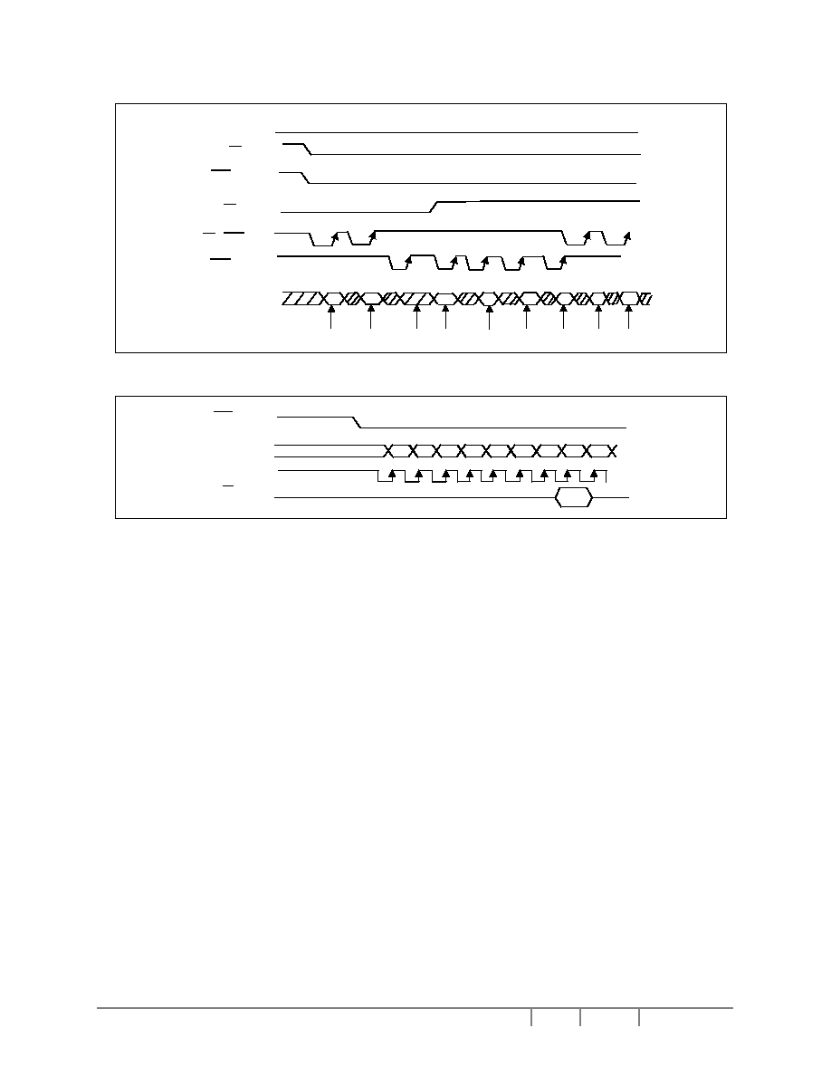
Display Data RAM (DDRAM)
DDRAM stores display data of maximum 64 x 8 bits (Max 64 characters). DDRAM address is set in the address
counter as a hexadecimal number.
Figure 9 - DDRAM Address
00 01 02 03 04 05 06 07 08 09 0A 0B 0C 0D 0E 0F
10 11 12 13 14 15 16 17 18 19 1A 1B 1C 1D 1E 1F
20 22 22 23 24 25 26 27 28 29 2A 2B 2C 2D 2E 2F
30 33 32 33 34 35 36 37 38 39 3A 3B 3C 3D 3E 3F
00 01 02 03 04 05 06 07 08 09 0A 0B 0C 0D 0E 0F
10 11 12 13 14 15 16 17 18 19 1A 1B 1C 1D 1E 1F
20 22 22 23 24 25 26 27 28 29 2A 2B 2C 2D 2E 2F
30 33 32 33 34 35 36 37 38 39 3A 3B 3C 3D 3E 3F
SEGMENT ICON RAM (ICONRAM)
ICONRAM has segment control data and segment pattern data. There are 2 ICONS pins (COMI0 & COMI1), which
has the same signal. So the icons on the same SEG are displayed at the same time. The number of icons is 80.
Table 4 - Relationship between ICONRAM Address and Display Pattern
ICONRAM bits
ICONRAM address
D7 D6 D5 D4 D3 D2 D1 D0
00h
- - - S0 S1 S2 S3 S4
01h
- - - S5 S6 S7 S8 S9
02h
- -
- S10 S11 S12 S13 S14
...
... ... ... ... ... ... ... ...
0Dh
- -
- S65 S66 S67 S68 S69
0Eh
- -
- S70 S71 S72 S73 S74
0Fh
- -
- S75 S76 S77 S78 S79
Note: "-": Don't care.
Character Generator ROM (CGROM)
CGROM has 5 x 8 dot 256 characters. The Function Set instruction selects the 8 characters (00h - 07h) of CGROM
or CGRAM.
1
st
Ch
16
th
Ch
SEG 0
SEG 79
COM0 � COM7
COM8 � COM15
Hidden Line
Hidden Line
1
st
Ch
16
th
Ch
SEG 0
SEG 79
COM0 � COM7
COM8 � COM15
COM16 � COM23
Hidden Line
(1) 2 line mode DDRAM Address
(2) 3 line mode DDRAM Address

Solomon Systech
Jan 2003
P 16/41 Rev 1.1
SSD1801
Table 5 -
CGROM Character Code
Note: The CGROM 0000xxxx are empty.
SSD1801
Rev 1.1
P 17/41 Jan 2003
Solomon Systech
Character Generator RAM (CGRAM)
CGRAM has up to 5 x 8 dots 8 characters. By writing font data to CGRAM, user defined character can be used.
CGRAM can be written regardless of Function Set instruction.
Table 6 -
Relationship between Character Code (DDRAM) and Character Pattern (CGRAM)
ICONRAM bits
Character Code
(DDRAM data)
CGRAM address
D7 D6 D5 D4 D3 D2 D1 D0
00h (Pattern 0)
40h
41h
42h
43h
44h
45h
46h
47h
-
-
-
-
-
-
-
-
-
-
-
-
-
-
-
-
-
-
-
-
-
X
X
X
X
X
X
X
X
X
X
X
X
X
X
X
X
X
X
X
X
X
X
X
X
X
X
X
X
X
X
X
X
X
X
X
01h (Pattern 1)
48h
49h
4Ah
4Bh
4Ch
4Dh
4Eh
4Fh
-
-
-
-
-
-
-
-
-
-
-
-
-
-
-
-
-
-
-
-
-
X
X
X
X
X
X
X
X
X
X
X
X
X
X
X
X
X
X
X
X
X
X
X
X
X
X
X
X
X
X
X
X
X
X
X
02h (Pattern 2)
50h
51h
52h
53h
54h
55h
56h
57h
-
-
-
-
-
-
-
-
-
-
-
-
-
-
-
-
-
-
-
-
-
X
X
X
X
X
X
X
X
X
X
X
X
X
X
X
X
X
X
X
X
X
X
X
X
X
X
X
X
X
X
X
X
X
X
X
03h (Pattern 3)
58h
59h
5Ah
5Bh
5Ch
5Dh
5Eh
5Fh
-
-
-
-
-
-
-
-
-
-
-
-
-
-
-
-
-
-
-
-
-
X
X
X
X
X
X
X
X
X
X
X
X
X
X
X
X
X
X
X
X
X
X
X
X
X
X
X
X
X
X
X
X
X
X
X
04h (Pattern 4)
60h
61h
62h
63h
64h
65h
66h
67h
-
-
-
-
-
-
-
-
-
-
-
-
-
-
-
-
-
-
-
-
-
X
X
X
X
X
X
X
X
X
X
X
X
X
X
X
X
X
X
X
X
X
X
X
X
X
X
X
X
X
X
X
X
X
X
X
05h (Pattern 5)
68h
69h
6Ah
6Bh
6Ch
6Dh
6Eh
6Fh
-
-
-
-
-
-
-
-
-
-
-
-
-
-
-
-
-
-
-
-
-
X
X
X
X
X
X
X
X
X
X
X
X
X
X
X
X
X
X
X
X
X
X
X
X
X
X
X
X
X
X
X
X
X
X
X

Solomon Systech
Jan 2003
P 18/41 Rev 1.1
SSD1801
06h (Pattern 6)
70h
71h
72h
73h
74h
75h
76h
77h
-
-
-
-
-
-
-
-
-
-
-
-
-
-
-
-
-
-
-
-
-
X
X
X
X
X
X
X
X
X
X
X
X
X
X
X
X
X
X
X
X
X
X
X
X
X
X
X
X
X
X
X
X
X
X
X
07h (Pattern 7)
78h
79h
7Ah
7Bh
7Ch
7Dh
7Eh
7Fh
-
-
-
-
-
-
-
-
-
-
-
-
-
-
-
-
-
-
-
-
-
X
X
X
X
X
X
X
X
X
X
X
X
X
X
X
X
X
X
X
X
X
X
X
X
X
X
X
X
X
X
X
X
X
X
X
NOTE: "-" Don't use
"X" Pattern 0 or 1
LCD Driving Voltage Generator and Regulator
This module generates the LCD voltage required for display driving output. It takes a single supply input and
generates necessary voltage levels. This block consists of:
1. 2x/3x DC-DC voltage converter
The built-in Regulated DC-DC voltage converter is used to generate positive LCD driving voltage with reference
to AV
SS
. For SSD1801, it is possible to produce boosting from the internal reference voltage V
REF
. Detail
configurations of the DC-DC converter for boosting are given in Figure 10.
Figure 10 � Configurations for DC-DC Converter
SSD1801 SSD1801
AVDD
C1P
C1N
C2P
VOUT
AVDD
C1P
C1N
C2P
C2N
VOUT
C1
+
+
C2
+
C2
C1
+
+
C2
C2
+
AVDD
AVDD
3x DC-DC Converter 2x DC-DC Converter
Remarks:
C1 = 2.2
�F - 4.7�F
C2 = 0.1
�F - 1�F
Figure 11 - Configurations for Voltage Regulator
DC-DC
Converter
R2
REF
R1
AVss
V
REF
V
OUT
/
V
L6
V
EXT
V
F
+
-
Remarks:
R1 and R2 = 500K-2.5M ohms

SSD1801
Rev 1.1
P 19/41 Jan 2003
Solomon Systech
2. Voltage Regulator
The feedback gain control for LCD driving contrast can be adjusted by using reference voltage and external
resistor network. The reference voltage is selected by REF pin. When it is pulled low, internal voltage reference
V
REF
is used. When it is pulled high, external voltage reference V
EXT
will be in use. The external resistors are
required to be connected between AV
SS
and V
F
(R1), and between V
F
and V
L6
(R2). The following equations are
used to calculate the regulator output voltages.
When REF is low:
REF
L
out
V
R
R
V
V
�
+
=
=
1
2
1
6
AND
06
.
0
2
�
= V
V
REF
When REF is high:
EXT
6
L
out
V
1
R
2
R
1
V
V
�
+
=
=
3. Contrast Control
Software control of the 32 contrast voltage levels at each voltage regulator feedback gain. The equation of calculating
the LCD driving voltage is given as:
When REF is low:
-
�
�
+
=
=
150
1
1
2
1
6
n
V
R
R
V
V
REF
L
out
When REF is high:
-
�
�
+
=
=
150
1
1
2
1
6
n
V
R
R
V
V
EXT
L
out
where n is set in contrast control register.
Table 7- Contrast Control Register
No. X7 X6 X5 X4 X3 X2 X1 X0
n
Vout Contrast
1 - - - 0 0 0 0 0 0
(default)
Maximum High
2 - - - 0 0 0 0 1
1
3 - - - 0 0 0 1 0
2
4 - - - 0 0 0 1 1
3
.
.
.
.
.
.
.
.
.
-
-
-
-
-
-
-
-
-
.
.
.
.
.
.
.
.
.
.
.
.
.
.
.
.
.
.
.
.
.
.
.
.
31 - - - 1 1 1 1 0
30
.
.
32 1 1 1 1 1
31
Minimum Low
(" - ": Don't care)
4. Bias Divider
Divide the regulator output to give the LCD driving voltages (V
L5
-V
L2
). A low power consumption circuit design in
this bias divider saves most of the display current comparing to traditional design.
5. Bias Ratio Selection circuitry

Solomon Systech
Jan 2003
P 20/41 Rev 1.1
SSD1801
Software control of 1/4 and 1/5 bias ratio to match the characteristic of LCD panel.
Reset Circuit
This block includes Power On Reset circuitry and the Reset pin RES . Both of these having the same reset
function. Once RES receives a negative reset pulse, all internal circuitry will start to initialize. Minimum pulse width
for completing the reset sequence is 10ms.
The status of the chip after reset is given by:
1. Display/ cursor/ blink is turned OFF
2. 2-line display mode
3. Power control register is set to 000b
4. Oscillator is OFF
5. Power save is OFF
6. CGRAM is not used
7. Shift register data clear in serial interface
8. Bias ratio is set to 1/5
9. Address counter is set to 00h
10. Normal scan direction of the COM outputs
11. Contrast control register is set to 00h
12. Test mode is turned OFF
13. In case of 4-bit interface mode selection, SSD1801 considers the 1st 4-bit data from MPU as the
high order bits.
14. The 1st line of display is the address 00h-0Fh.
Display Data Latch
A series of registers carrying the display signal information. For SSD1801, there are 105 latches (80 + 25) for
holding the data, which will be fed to the HV Buffer Cell and Level Selector to output the required voltage levels.
Level Selector
Level Selector is a control of the display synchronization. Display voltage can be separated into two sets and
used with different cycles. Synchronization is important since it selects the required LCD voltage level to the HV
Buffer Cell, which in turn outputs the COM or SEG LCD waveform.
HV Buffer Cell (Level Shifter)
Buffer Cell work as a level shifter which translates the low voltage output signal to the required driving voltage.
The output is shifted out with an internal FRM clock which comes from the Display Timing Generator. The voltage
levels are given by the level selector which is synchronized with the internal M signal.

SSD1801
Rev 1.1
P 21/41 Jan 2003
Solomon Systech
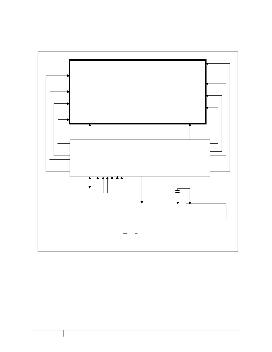
VOLTAGE GENERATOR CIRCUIT
Figure 12 � When Built � in Power Supply is used
Figure 13 � When External Power Supply is used
VDD
3x DC-DC Converter
2x DC-DC Converter
Remarks:
(VC,VF = 1,1)
Note: VC, VF = bit X
2
and X
0
in the command of Power Control Register;
C1 = 2.2
�F - 4.7�F
X
2
is the bit of turns on/off of the internal voltage converter and regulator
C2 = 0.1
�F - 1�F
X
0
is the bit of turns on/off of the voltage divider
R1 and R2 = 500K-2.5M ohms
R1
AVDD
C1P
C1N
C2P
C2N
VOUT
VF
VL6
VL5
VL4
VL3
VL2
AVSS
+
C2
+
C2
VDD
C1
+
GND
R2
GND
AVDD
C1P
C1N
C2P
VOUT
VF
VL6
VL5
VL4
VL3
VL2
AVSS
+
C2
C2
+
C1
+
GND
R1
R2
GND
Solomon Systech
Jan 2003
P 22/41 Rev 1.1
SSD1801
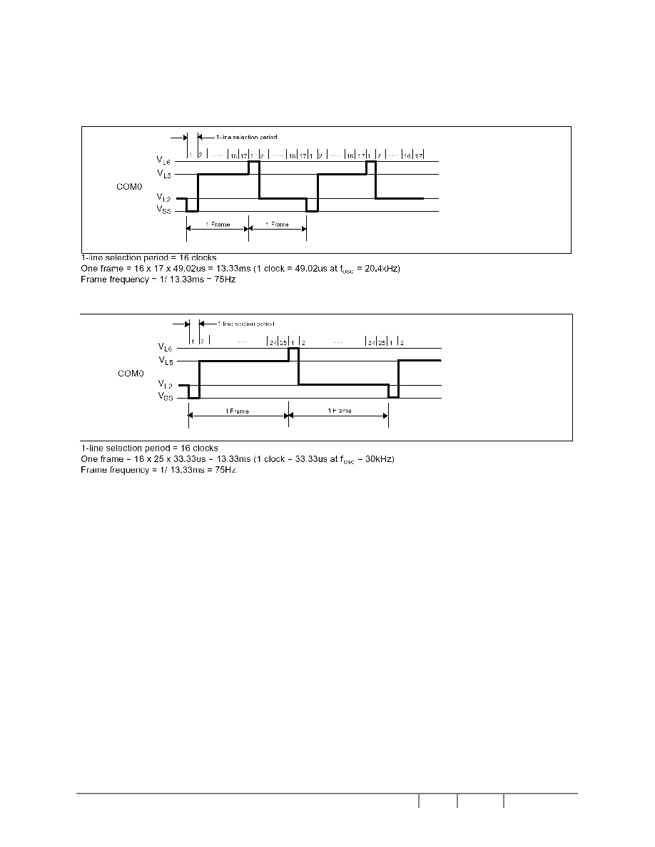
FRAME FREQUENCY
2-line mode (1/17 Duty)
3-line mode (1/25 Duty)

SSD1801
Rev 1.1
P 23/41 Jan 2003
Solomon Systech
COMMAND TABLE
Table 8 - Command Table
Bit Pattern
Instruction
Description
0000001X
0
Return Home
DDRAM address is set to 00h from address counter and the cursor
returns to 00h position
The contents of DDRAM are not changed.
000010X
1
X
0
Set Double Height Mode
X
1
X
0
= 00: normal display (POR)
X
1
X
0
= 01: COM0 - COM15 is double height
COM16 - COM23 is normal
X
1
X
0
= 10: 1) 2-line mode: normal display
2) 3-line mode: COM0 -COM7 is normal
COM8 - COM23 is double height
X
1
X
0
= 11: normal display
000011X
1
X
0
Set Power Save Mode / Oscillator Control
X
0
= 0: power save OFF (POR)
X
0
= 1: power save ON
X
1
= 0: oscillator OFF (POR)
X
1
= 1: oscillator ON
00010X
2
X
1
X
0
Function Set
X
0
= 0: CGROM is selected (POR)
X
0
= 1: CGRAM is selected
X
1
= 0: 1) 2-line mode: COM0 -> COM15 (POR)
2) 3-line mode: COM0 -> COM23 (POR)
X
1
= 1: 1) 2-line mode: COM15 -> COM0
2) 3-line mode: COM23 -> COM0
X
2
= 0: 2-line display mode (POR)
X
2
= 1: 3-line display mode
000110X
1
X
0
Set Display Start Line
X
1
X
0
= 00: DDRAM line 1 shows at the first line of LCD (POR).
X
1
X
0
= 01: DDRAM line 2 shows at the first line of LCD.
X
1
X
0
= 10: DDRAM line 3 shows at the first line of LCD.
X
1
X
0
= 11: DDRAM line 4 shows at the first line of LCD.
000111*X
0
Set Bias Control
X
0
= 0: 1/5 bias (POR)
X
0
= 1: 1/4 bias
00100X
2
X
1
X
0
Set Power Control Register
X
0
= 0: turns off the voltage divider (POR)
X
0
= 1: turns on the voltage divider
X
1
: Don't care
X
2
= 0: turns off the internal voltage converter and regulator (POR)
X
2
= 1: turns on the internal voltage converter and regulator
00101X
2
X
1
X
0
Set Display Control
X
0
= 0: turns off the display (POR)
X
0
= 1: turns on the display
X
1
= 0: blink off (POR)
X
1
= 1: blink on
X
2
= 0: cursor off (POR)
X
2
= 1: cursor on
1X
6
X
5
X
4
X
3
X
2
X
1
X
0
Set DD/CGRAM address
DDRAM/ CGRAM address range:
DDRAM: 00h - 3Fh
CGRAM: 40h - 7Fh
010X
4
X
3
X
2
X
1
X
0
Set ICONRAM address / Contrast Control
ICONRAM address range / Contrast Control Register:
ICONRAM: 00h - 0Fh
Contrast Control Register: 10h
TE: 11h (test byte)
00000000
NOP
Command for No Operation
0011****
Set Test Mode
Reserved for IC testing. Do Not use.
Note:
1. Patterns other than that given in Command Table are prohibited to enter to the chip as a command. Otherwise, unexpected result
will occur.
2. "*" : Don't care.

Solomon Systech
Jan 2003
P 24/41 Rev 1.1
SSD1801
Data Read/ Write
To read data from the internal memories (DDRAM/ CGRAM/ ICONRAM), input high to R/W ( WR ) pin and D/ C
pin for 6800-series parallel mode, low to E( RD ) pin and high to D/ C pin for 8080-series parallel mode. No data read
is provided for serial mode. In normal mode, address counter will be increased by one automatically after each data
read. A dummy read is required before the first data read. See Figure 4 in Functional Description.
To write data to the internal memories (DDRAM/ CGRAM/ ICONRAM), input low to R/W ( WR ) pin and high to
D/ C pin for 6800-series and 8080-series parallel mode. For serial interface, it will always be in write mode. Address
counter will be increased by one automatically after each data write.

SSD1801
Rev 1.1
P 25/41 Jan 2003
Solomon Systech
COMMAND DESCRIPTIONS
Return Home
Return Home instruction field makes cursor return home. DDRAM address is set to 00h from address counter
and the cursor returns to 00h position. The contents of DDRAM are not changed.
Set Double Height Mode
This command increases the height of one character line from 8 to 16 dots. If the number of COM signal needed
exceeds the existing COM signal (COM0-COM15 for 2-line mode, COM0-COM23 for 3-line mode), the last character
line will not be displayed. It will happen at following cases:
1. 3-line mode, X
1
X
0
= 01 where COM0-COM15 is double height, COM16-COM23 is normal.
The 3rd line will not be displayed.
2. 3-line mode, X
1
X
0
= 10 where COM0-COM7 is normal, COM8-COM23 is double height.
The 3rd line will be displayed.
3.
2-line mode, X
1
X
0
= 01 where COM0-COM15 is double height.
The 2nd line will not be displayed.
Figure 14 � 3-line Normal Mode Display in 3-line mode (X
1
X
0
= 00)
Figure 15 � COM0 ~ COM15 is a Double Height Line, COM16 ~COM23 is Normal in 3-line mode
(X
1
X
0
= 01)

Solomon Systech
Jan 2003
P 26/41 Rev 1.1
SSD1801
Figure 16 � COM0 ~ COM7 is Normal, COM8 ~ COM23 is a Double Height Line in 3-line mode (X
1
X
0
= 10)
Figure 17 � 2-line Normal Mode Display in 2-line mode (X
1
X
0
= 00)
Figure 18 � COM0 ~ COM15 is a Double Height Line in 2-line mode (X
1
X
0
= 01)

SSD1801
Rev 1.1
P 27/41 Jan 2003
Solomon Systech
Set Power Save Mode / Oscillator Control
To enter Standby or Sleep Mode, it should be done by turning off the internal oscillator and turning on the power
save control bit. The corresponding control bits are X
1
X
0
= 01. In order to put the system into low power consumption
mode, internal voltage converter, voltage regulator and voltage divider should also be turned off by using Power
Control Register. After putting the system into power save mode, the following status will be entered:
1. Internal oscillator and LCD power supply circuits are stopped.
2. Segment and Common drivers output AV
SS
level.
3. The display data and operation mode before sleep are held. All the internal circuit are stopped.
Function Set
This command sets 3 functions on the system. They are the number of display line (2 or 3), COM shift direction
(left or right) and CGROM/ CGRAM character area select.
Set Display Start Line
This command is to set Display Start Line register to determine starting address of display data RAM to be
displayed by selecting a value from 0 to 3. With the value equals to 0, the display will start from address (00h-0Fh).
With the value equals to 1, the display will start from address (10h-1Fh). With the value equals to 2, the display will
start from address (20h-2Fh). With the value equals to 3, the display will start from address (30-3Fh).
Set Bias Control
Bias ratio 1/4 or 1/5 could be set using this command. When changing the number of line display, the bias ratio
also needs to be adjusted to make display contrast consistent.
Set Power Control Register
This command turns on / off the various power circuits associated with the chip which including regulated DC-DC
converter and voltage divider.
Set Display Control
This command provides 3 display functions. It turns on/off both the cursor, blink and display. When both cursor
and blink control bit set high, the driver make LCD alternate between inverting display character and normal display
character at the cursor position with about a half second. On the contrary, if cursor control bit is low, only a normal
character is displayed regardless of blink control bit.

Solomon Systech
Jan 2003
P 28/41 Rev 1.1
SSD1801
X
2
, X
1
Display State
1, 0 (Cursor Mode)
1, 1 (Blinking Mode)
0, 0
0, 1
Figure 19 - Display Attributes
Set DD/ CGRAM Address
Before writing/ reading data into/ from the RAM, set the address by RAM address set instruction. Next, when
data are written/ read in succession, the address is automatically increased by1. After accessing 7Fh, the address is
00h.
Table 9 - DD/ CGRAM Address Mapping
ADDRESS 0 1 2 3 4 5 6 7 8 9 A B C D E F
00H
DDRAM LINE 1 (00H - 0FH)
10H
DDRAM LINE 2 (10H - 1FH)
20H
DDRAM LINE 3 (20H - 2FH)
30H
DDRAM LINE 4 (30H - 3FH)
40H
CGRAM (PATTERN 0)
CGRAM (PATTERN 1)
50H
CGRAM (PATTERN 2)
CGRAM (PATTERN 3)
60H
CGRAM (PATTERN 4)
CGRAM (PATTERN 5)
70H
CGRAM (PATTERN 6)
CGRAM (PATTERN 7)

SSD1801
Rev 1.1
P 29/41 Jan 2003
Solomon Systech
Set ICONRAM Address Set
Before writing/ reading data into/ from the ICONRAM, set the address by ICONRAM Address Set instruction.
Next, when data are written/ read in succession, the address is automatically increased by 1. The 5 icons at a time
can blink if blinking is enabled. The blink attributes of ICON are the same as the cursor blink. For accessing DD/
CGRAM, the DD/ CGRAM Address Set instruction should be set before. After accessing 0Fh, the address of
ICONRAM address is 00h. The ICONRAM address ranges are 00h-0Fh.
Table 10 - ICONRAM Address Mapping
ADDRESS 0 1 2 3 4 5 6 7 8 9 A B C D E F
00H
ICONRAM (00h - 0Fh)
10H
C
C
R
T
E
Reserved
Set Contrast Control Register
Set the Contrast Control Register (CCR) by ICONRAM Address Set Instruction. Next, data are written to the
CCR. The default value of CCR is (00000).
TE: Test Mode Register (Do not Use) (11H)
When the CCR and TE registers are written, the address counter is not increased.
NOP
A command causing No Operation.
Set Test Mode
This command force the driver chip into its test mode for internal testing of the chip. Under normal operation, user
should NOT use this command.
Solomon Systech
Jan 2003
P 30/41 Rev 1.1
SSD1801
MAXIMUM RATINGS
Table 11 - Maximum Ratings
(Voltage Reference to VSS)
Symbol
Parameter
Value
Unit
AV
DD,
DV
DD
Supply Voltage
-0.3 to +4.0V
V
VL6
VLCD Voltage
-0.3 to +6.5V
V
V
IN
Input Voltage
V
SS
-0.3 to
V
DD
+0.3
V
T
A
Operating Temperature
-30 to +85
�C
T
stg
Storage Temperature Range
-65 to +150
�C
* Maximum Ratings are those values beyond which damage to the device may occur. Functional
operation should be restricted to the limits in the Electrical Characteristics tables or Pin Description
section
This device contains circuitry to protect the inputs against damage due to high static voltages or electric
fields; however, it is advised that normal precautions to be taken to avoid application of any voltage
higher than maximum rated voltages to this high impedance circuit. For proper operation it is
recommended that V
in
and V
out
be constrained to the range V
SS
< or = (V
in
or V
out
) < or = V
DD.
Reliability of operation is enhanced if unused inputs are connected to an appropriate logic voltage level
(e.g., either V
ss
or V
DD
). Unused outputs must be left open. This device may be light sensitive. Caution
should be taken to avoid exposure of this device to any light source during normal operation. This device
is not radiation protected.
SSD1801
Rev 1.1
P 31/41 Jan 2003
Solomon Systech
DC CHARACTERISTICS
Table 12 - DC Characteristics
(Unless otherwise specified, Voltage Referenced to VSS, VDD = 2.4 to
3.6V, TA = -30 to 85�C.)
Symbol Parameter
Test
Condition Min
Typ
Max
Unit
DVDD
AVDD
Logic and Analog Circuit
Supply Voltage Range
(Absolute value referenced to
DVss and AVss)
2.4 2.7 3.6
V
IDD1
IDD2
ISB
Display Operation Supply
Current Drain
Access operation from MPU
Supply Current Drain
Standby Mode Supply Current
VDD = 3V, TA = 25�C
VLCD = 5.8V without load
No access from MPU
VDD = 3V, TA = 25�C
fcyc = 200kHz
Current No load
Oscillator OFF
Power Save ON
-
-
-
-
-
-
85
500
5
�A
�A
�A
V
LCD
V
OUT
LCD Driving Voltage Input
Voltage Converter Output
Voltage
VLCD = VL6 - VSS
TA = 25�C, C = 1uF
4
AVDD
-
-
5.8
5.8
V
V
VIH
VIL
Logic High Input Voltage
Logic Low Input Voltage
0.8*DVDD
0
-
-
DVDD
0.2*DVDD
V
V
VOH
VOL
VL6
VL6
Logic High Output Voltage
Logic Low Output Voltage
LCD Driving Voltage Source
(VL6)
LCD Driving Voltage Source
(VL6)
IOH = -1mA, VDD = 2.4V
IOL = 1mA, VDD = 2.4V
Regulator Enable (VL6 voltage
depends on contrast control/
external resistors network)
Regulator Disable
DVDD � 0.4
-
AVSS - 0.5
-
-
-
-
Floating
-
0.4
Vout
-
V
V
V
V
V
L
6
V
L
5
V
L4
V
L3
V
L2
V
L
6
V
L
5
V
L4
V
L3
V
L2
LCD Display Voltage Output
(V
L5
, V
L4
, V
L3
, V
L2
)
LCD Display Voltage Output
(V
L5
, V
L4
, V
L3
, V
L2
)
Voltage reference to AV
SS
,
Bias Divider Enabled, 1:a
bias ratio
Voltage reference to AV
SS
,
External Voltage Generator,
Bias Divider Disable
-
-
-
-
-
V
L
5
V
L4
V
L3
V
L2
V
SS
V
L6
(a-1)/a * V
L6
(a-2)/a * V
L6
2/a * V
L6
1/a * V
L6
-
-
-
-
-
-
-
-
-
-
5.8
V
L
6
V
L
5
V
L4
V
L3
V
V
V
V
V
V
V
V
V
V
I
OH
I
OL
I
OZ
Logic High Output Current
Source
Logic Low Output Current
Drain
Logic Output Tri-state Current
Drain Source
VOUT = VDD - 0.4V
VOUT = 0.4V
50
-
-1
-
-
-
-
-50
1
�A
�A
�A
I
IL
/ I
IH
Logic Input Current
-1
-
1
�A
C
IN
Logic Pins Input Capacitance
-
5
7.5
PF

Solomon Systech
Jan 2003
P 32/41 Rev 1.1
SSD1801
Symbol Parameter
Test
Condition Min
Typ
Max
Unit
Vref
Vext
Voltage regulator reference
voltage
External voltage reference
1.94
1.2
2
2
2.06
VDD
V
V
SSD1801
Rev 1.1
P 33/41 Jan 2003
Solomon Systech
AC CHARACTERISTICS
Table 13 - AC Characteristics (Unless otherwise specified, Voltage Referenced to VSS, VDD = 2.4 to
3.6V, TA = -30 to 85�C.)
Symbol Parameter
Test
Condition Min
Typ
Max
Unit
F
FRM
Frame Frequency
Internal Oscillator
V
DD
= 3V, T
A
= 25
�
C
67.5
75
90
Hz
Table 14 - 6800-Series MPU Parallel Interface Timing Characteristics (VDD - VSS = 2.4 to 3.6V, TA =
-30 to 85�C)
Symbol
Parameter
Min Typ Max Unit
t
cycle
Clock
Cycle
Time
650 - - ns
t
AS
Address Setup Time
60
-
-
ns
t
AH
Address
Hold
Time
30 - -
Ns
t
DSW
Write Data Setup Time
100
-
-
Ns
t
DHW
Write Data Hold Time
50
-
-
Ns
t
DHR
Read Data Hold Time
50
-
-
ns
t
OH
Output
Disable
Time
- -
70
ns
t
ACC
Access
Time
- -
100
ns
E( RD )
Low Pulse Width (read)
150 - - ns
PW
EL
E( RD )
Low Pulse Width (write)
150 - - ns
E( RD )
High Pulse Width (read)
450 - - ns
PW
EH
E( RD )
High Pulse Width (write)
450 - - ns
t
R
Rise
Time
- -
25
ns
t
F
Fall
Time
- -
25
ns

Solomon Systech
Jan 2003
P 34/41 Rev 1.1
SSD1801
Figure 20 � 6800-series MCU Parallel Interface Waveform

SSD1801
Rev 1.1
P 35/41 Jan 2003
Solomon Systech
Table 15 - 8080-Series MPU Parallel Interface Timing Characteristics (VDD - VSS = 2.4 to 3.6V, TA =
-30 to 85�C)
Symbol
Parameter
Min Typ Max Unit
t
cycle
Clock
Cycle
Time
650 - - ns
t
AS
Address Setup Time
60
-
-
ns
t
AH
Address
Hold
Time
30 - -
ns
t
DSW
Write Data Setup Time
100
-
-
ns
t
DHW
Write Data Hold Time
50
-
-
ns
t
DHR
Read Data Hold Time
50
-
-
ns
t
OH
Output
Disable
Time
- -
70
ns
t
ACC
Access
Time
- -
100
ns
WR
Low Pulse Width (read)
450 - - ns
PW
WRL
WR
Low Pulse Width (write)
450 - - ns
WR
High Pulse Width (read)
150 - - ns
PW
WRH
WR
High Pulse Width (write)
150 - - ns
t
R
Rise
Time
- -
25
ns
t
F
Fall
Time
- -
25
ns
Figure 21 � 8080-series MCU Parallel Interface Waveform
Solomon Systech
Jan 2003
P 36/41 Rev 1.1
SSD1801
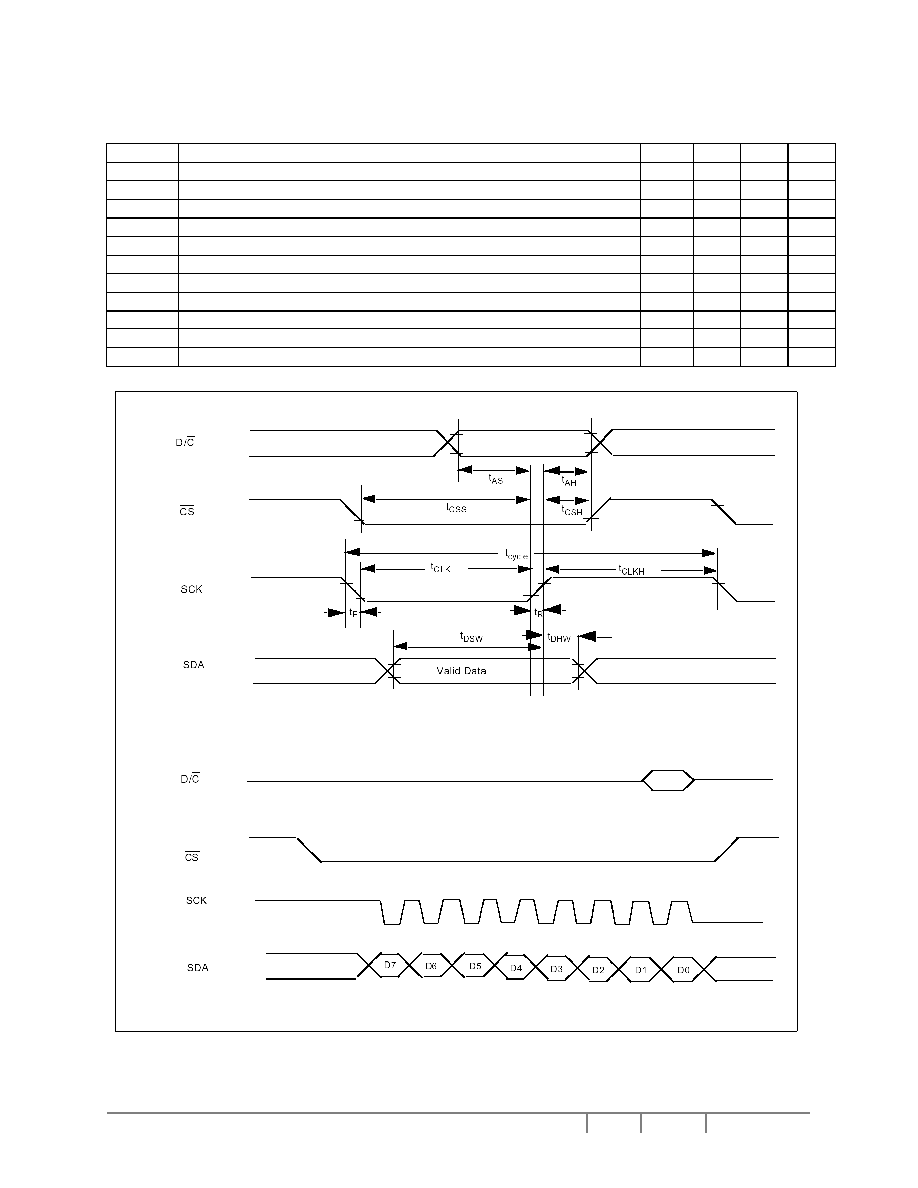
Table 16 - Serial Interface Timing Characteristics (VDD - VSS = 2.4 to 3.6V, TA = -30 to 85�C)
Symbol
Parameter
Min Typ Max Unit
t
cycle
Clock
Cycle
Time
1000
- - ns
t
AS
Address Setup Time
50
-
-
ns
t
AH
Address
Hold
Time
300
- -
ns
t
CSS
Chip Select Setup Time
150
-
-
ns
t
CSH
Chip Select Hold Time
700
-
-
ns
t
DSW
Write Data Setup Time
50
-
-
ns
t
DHW
Write Data Hold Time
50
-
-
ns
t
CLKL
Clock
Low
Time
300 - - ns
t
CLKH
Clock
High
Time
300 - - ns
t
R
Rise
Time
- -
25
ns
t
F
Fall
Time
- -
25
ns
Figure 22 � Serial Interface Characteristics
SSD1801
Rev 1.1
P 37/41 Jan 2003
Solomon Systech
APPLICATION EXAMPLES
Figure 23 - Application Circuit: External Regulator with internal divider mode (8-bit 6800 mode)
SSD1801 IC
24 MUX
(DIE FACE IP)
SEG79.......................................................................................SEG0
COMI1
COM23
COM22
COM21
COM20
COM15
COM14
:
:
COM9
COM8
COM19
COM18
COM17
COM16
COM7
COM6
COM5
:
:
COM0
COMI0
SEG0..................................................................SEG79
DISPLAY PANEL SIZE
80 X 24 + 1 ICON LINE
COM8
COM9
:
:
COM14
COM15
:
:
COM20
COM21
COM22
COM23
COMI1
COMI0
COM0
COM1
:
:
COM6
COM7
:
:
COM16
COM17
COM18
COM19
D0-D7
D
VSS & AVSS[
GN
D
]
VDD=3.0V
AVSS
0.1uF +
DVDD VL2 VL3 VL4 VL5 VL6
AVDD
External Power Supply
Logic pin connections not specified above:
Pins connected to DVdd: C68/ 80 , P/ S , DL, DIRS
Pins connected to DVss: REF, CLK
E
(
/
RD)
/C
S
/R
ES
D/#
C
R/
W (#WR)
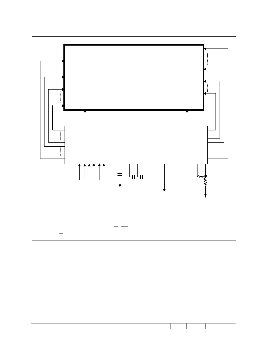
Solomon Systech
Jan 2003
P 38/41 Rev 1.1
SSD1801
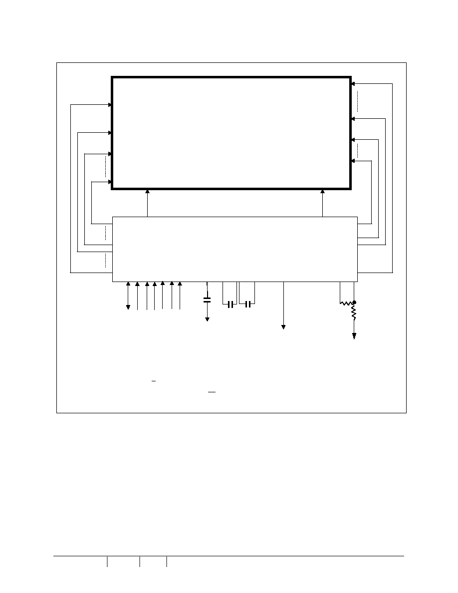
Figure 24 - Application Circuit: ALL internal power mode with 2x regulated DC-DC converter
(serial mode)
Logic pin connections not specified above:
Pins connected to DVdd: DL, DIRS
Pins connected to DVss: REF, CLK, P/ S , R/W ( WR ),
E(/RD), C68/ 80 , D5-D0
SSD1801 IC
24 MUX
(DIE FACE IP)
SEG79.......................................................................................SEG0
COMI1
COM23
COM22
COM21
COM20
COM15
COM14
:
:
COM9
COM8
COM19
COM18
COM17
COM16
COM7
COM6
COM5
:
:
COM0
COMI0
SEG0..................................................................SEG79
DISPLAY PANEL SIZE
80 X 24 + 1 ICON LINE
COM8
COM9
:
:
COM14
COM15
:
:
COM20
COM21
COM22
COM23
COMI1
COMI0
COM0
COM1
:
:
COM6
COM7
:
:
COM16
COM17
COM18
COM19
SC
K (
D
6
)
SD
A (
D
7
)
D
VSS & AVSS[
GN
D
]
AVDD
VDD = 3.0V
DVDD VL2 VL3 VL4 VL5 VL6
AVDD
VOUT C1N C1P
C2P
R1
R2
VF
AVSS
Note:
It is recommended to use 2x regulated DC-DC
converter to reduce the current consumption
under certain of condition.
e.g. AV
DD
/DV
DD
= 3.0V and V
LCD
(LCD driving
voltage) = 5.0V.
+C1 C2
C2
C1: 2.2 -4.7 uF
C2: 0.1-1uF
/C
S
/R
ES
D/#
C
+ +
Remarks :
R1 and R2 = 500K-2.5M ohms
SSD1801
Rev 1.1
P 39/41 Jan 2003
Solomon Systech
Figure 25 - Application Circuit: ALL internal power mode with 3x regulated DC-DC converter
(8-bit 8080 mode)
Logic pin connections not specified above:
Pins connected to DVdd: P/ S , DL, DIRS
Pins connected to DVss: REF, CLK, and C68/( 80 )
SSD1801 IC
24 MUX
(DIE FACE IP)
SEG79.......................................................................................SEG0
COMI1
COM23
COM22
COM21
COM20
COM15
COM14
:
:
COM9
COM8
COM19
COM18
COM17
COM16
COM7
COM6
COM5
:
:
COM0
COMI0
SEG0..................................................................SEG79
DISPLAY PANEL SIZE
80 X 24 + 1 ICON LINE
COM8
COM9
:
:
COM14
COM15
:
:
COM20
COM21
COM22
COM23
COMI1
COMI0
COM0
COM1
:
:
COM6
COM7
:
:
COM16
COM17
COM18
COM19
D0-D7
E
(
/
RD)
/C
S
/R
ES
D
VSS & AVSS[
GN
D
]
D/#
C
AVDD
VDD = 3.0V
DVDD VL2 VL3 VL4 VL5 VL6
AVDD
VOUT C1N C1P C2N C2P
R1
R2
VF
AVSS
R/
W (#WR)
+C1
C2 C2
C1: 2.2 -4.7 uF
C2: 0.1-1uF
+ +
Remarks :
R1 and R2 = 500K-2.5M ohms
Solomon Systech
Jan 2003
P 40/41 Rev 1.1
SSD1801
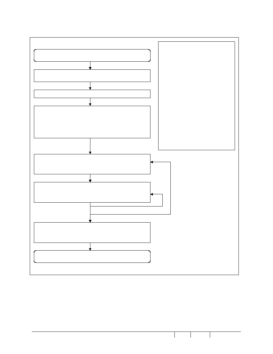
Recommended INITIALIZING of SSD1801
Figure 26 - Recommended INITIALIZING of SSD1801
DV
DD
/AV
CC
-DV
SS
/AV
SS
Power On
End of initialization
Send reset pulse to the RES pin.
(Recommended minimum reset pulse width is 10ms)
Waiting for 10usec
Command Input
1. Function set (00010X2X1X0)
2. Contrast control register setup
3. Power save (power save off; OSC on)
4. Power control (turns on the internal regulator and turns on the
internal divider)
Command Input
5. RAM address set
Data Input
6. Data writing (RAM clear)
(DDRAM=20h, CG/ICONRAM=00h)
Command Input
7. Display control (turns on the display) (There is an auto mask
off period ~ 260ms)
NOTE:
At instructions 1-6, the minimum clock cycle
time is 650ns for PPI. For details, pls refer
to the SSD1801 datasheet "AC
Characteristics".
At 5 and 6, the internal RAM should be
cleared.
To clear DDRAM, set address at 00h (first
DDRAM) and then write 20h (space
character code) 64times.
To clear CGRAM, set address at 40h (first
CGRAM) and then write 00h (null data) 64
times
To clear ICONRAM, set CONRAM address
at 00h (first ICONRAM) and then write 00h
(null data) 16 times
No delay between each Command/Data
input under ideal timing situation (No time
shift in any signals, refer to page 32 for
details )

SSD1801
Rev 1.1
P 41/41 Jan 2003
Solomon Systech
Solomon Systech reserves the right to make changes without further notice to any products herein. Solomon Systech makes no warranty,
representation or guarantee regarding the suitability of its products for any particular purpose, nor does Solomon Systech assume any liability arising
out of the application or use of any product or circuit, and specifically disclaims any and all liability, including without limitation consequential or
incidental damages. "Typical" parameters can and do vary in different applications. All operating parameters, including "Typical" must be validated for
each customer application by customer's technical experts. Solomon Systech does not convey any license under its patent rights nor the rights of
others. Solomon Systech products are not designed, intended, or authorized for use as components in systems intended for surgical implant into the
body, or other applications intended to support or sustain life, or for any other application in which the failure of the Solomon Systech product could
create a situation where personal injury or death may occur. Should Buyer purchase or use Solomon Systech products for any such unintended or
unauthorized application, Buyer shall indemnify and hold Solomon Systech and its offices, employees, subsidiaries, affiliates, and distributors harmless
against all claims, costs, damages, and expenses, and reasonable attorney fees arising out of, directly or indirectly, any claim of personal injury or
death associated with such unintended or unauthorized use, even if such claim alleges that Solomon Systech was negligent regarding the design or
manufacture of the part.
http://www.solomon-systech.com