 | –≠–ª–µ–∫—Ç—Ä–æ–Ω–Ω—ã–π –∫–æ–º–ø–æ–Ω–µ–Ω—Ç: SSD1901 | –°–∫–∞—á–∞—Ç—å:  PDF PDF  ZIP ZIP |

This document contains information on a new product under definition stage. Solomon Systech Ltd. reserves the
right to change or discontinue this product without notice.
http://www.solomon-systech.com
SSD1901
Rev 1.1
Jul 2001
Copyright
©
2003
Solomon Systech Limited
SOLOMON SYSTECH
SEMICONDUCTOR TECHNICAL DATA
P 1/59
Advance Information
SSD1901 TFT Graphics Controller
1 GENERAL DESCRIPTION
The SSD1901 is a TFT graphics controller with an embedded 80K byte SRAM display memory. It supports high reso-
lution TFT panels with 8-bpp color depths, allowing up to 256 colors. The high integration of the SSD1901 provides a
low cost, low power, single chip solution to meet the requirements of embedded systems, such as Office Automation
equipment, Mobile Communications devices, and Hand-Held PCs where board size and battery life are major concerns.
The SSD1901supports Virtual, Split Screen and Floating Window display features to reduce the software manipulation.
It also provides Fixed Window to simplify the display data update process. The above features, combines with the Op-
erating System independence of the SSD1901 interface, make it the ideal solution for a wide variety of applications. It
also provides advantage of single power supply. The SSD1901 is available in a 80 pin QFP package.
This document contains information on a new product. Specifications and information herein are subject to change without notice .

SSD1901
Rev 1.1
Jul 2001
Solomon Systech
P 2/59
2 FEATURES
2.1 Integrated Display Memory
∑ Embedded 80K byte SRAM display memory.
2.2 CPU Interface
∑ Direct support of the following interfaces:
∑ Motorola MC68K.
∑ MPU bus interface using WAIT# signal.
∑ Direct memory mapping of internal registers into upper 128 bytes of 128K byte address space.
∑ The 80K byte display memory is directly and contiguously available through the 17-bit address bus.
2.3 Display Support
∑ 9/12 bits Active Matrix TFT interface
∑ Example resolutions: 160x160, 320x240
2.4 Display Modes
∑ 8 bit-per-pixel, 256-level color display.
∑ 256 simultaneous of 4096 colors on active matrix LCD panels.
∑ Virtual display support (displays images larger than the panel size through the use of panning and scrolling).
∑ Split screen display allows two different images to be simultaneously displayed.
∑ Fixed Window Mode simplifies the data update process for an image in a window area on the display.
∑ Floating Window Mode allows to display an image in a window area on the display without erasing the original image
data.
2.5 Clock Source
∑ Maximum input clock (CLKI) frequency of 50MHz.
∑ Maximum operating clock (CLK) frequency of 25MHz.
∑ Operating clock (CLK) is derived from CLKI or BCLK input.
∑ Pixel Clock (PCLK) and Memory Clock (MCLK) are derived from CLK.
2.6 Miscellaneous
∑ Software Color Invert.
∑ Software Power Saving mode.
∑ Hardware Power Saving mode.
∑ LCD power-down sequencing.
∑ 4 General Purpose Input/Output pins are available.
∑ GPIO0 is available if Hardware Power Saving is not required.
∑ GPIO[4:2] are available if 9 bit TFT panel is selected.
∑ Single Supply : 3.0 volts to 3.6 volts.

Solomon Systech
Jul 2001
Rev 1.1
SSD1901
P 3/59
3 ORDERING INFORMATION
Table 3-1 Ordering Information
Ordering Part Number
Package Form
SSD1901QL5
80 pin 12 x 12 x 1.4 mm LQFP package
SSD1901
Rev 1.1
Jul 2001
Solomon Systech
P 4/59
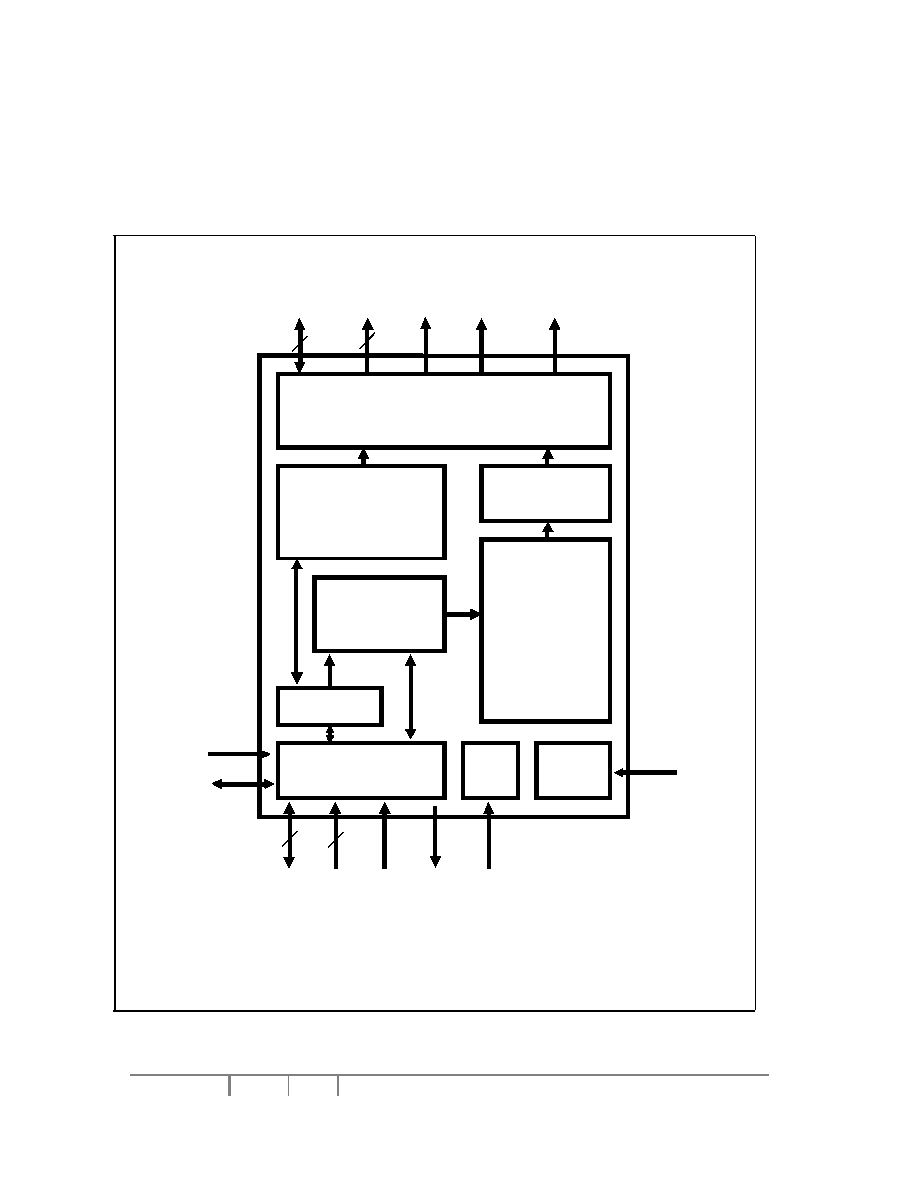
4 BLOCK DIAGRAM
4.1 Functional Block Descriptions
Figure 4-1 System Block Diagram
DB[15:0]
AB[16:1],
AB0
WE0#,
WE1#,
BS#, CS#,
RD/WR#,
RD#,
RESET#,
BCLK
HOST INTERFACE
CNF[3:0]
GPIO0
POWER
SAVE
CLOCKS
CLKI
Hardware
Power
Save
REGISTERS
MEMORY CONTROL
DISPLAY CONTROL
DISPLAY
MEMORY
LOOK UP
TABLE
LCD INTERFACE
FPDAT[8:0]
DRDY
FPSHIFT,
FPLINE,
FPFRAME
LCDPWR
WAIT#
FPDAT[11:9]

Solomon Systech
Jul 2001
Rev 1.1
SSD1901
P 5/59
5 FUNCTIONAL BLOCK DESCRIPTION
5.1 Host Interface
The Host Interface provides the means for the CPU to communicate with the display memory and internal registers.
5.2 Memory Control
The Memory Control arbitrates between CPU accesses and display refresh accesses. It also generates the necessary
signals to control the SRAM display memory.
5.3 Display Control
The Display Control manages data flow from the Memory Control through the Look-Up Table and to the LCD Interface.
It also generates memory addresses for display refresh accesses.
Display memory represents one pixel on the display. Figure 5-1 " Display Data Memory Organization" shows the display
data formats
5.4 Look - Up Table
The Look-Up Table contains three 256 entries, 4 bit wide Look-Up Tables or palettes, one for each primary color (red,
green and blue).
The following figures are intended to show the display data output path only.
Note
When Software Color Invert is enabled, the display data inverts after the Look-Up Table.
Figure 5-1 Display Data Memory Organization
P
0
P
1
P
2
P
3
P
4
P
5
P
6
P
7
P
8
P
9
Pn : RGB value from LUT index Mn
Panel Display
Display Memory
Byte 2
Byte 1
Byte 0
M
0
M
1
M
2
Host Address
LUT