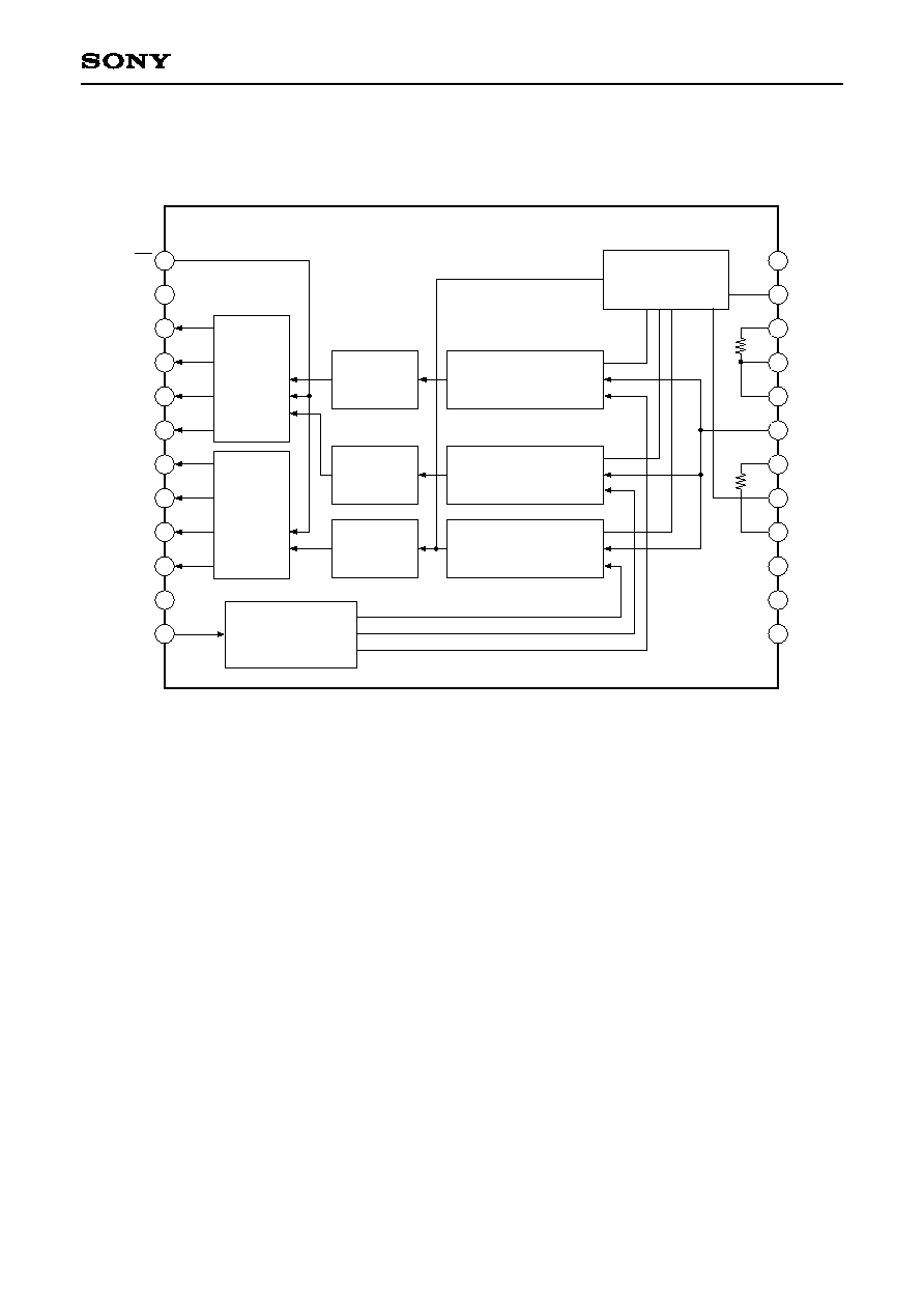
Description
The CXD1175A is an 8-bit CMOS A/D converter
for video use. The adoption of a 2-step parallel
system achieves low consumption at a maximum
conversion speed of 20MSPS minimum, 35MSPS
typical.
Features
∑ Resolution: 8 bit ± 1/2LSB (DL)
∑ Maximum sampling frequency: 20MSPS
∑ Low power consumption: 60mW (at 20MSPS typ.)
(reference current excluded)
∑ Built-in sampling and hold circuit
∑ Built-in reference voltage self-bias circuit
∑ 3-state TTL compatible output
∑ Power supply: 5V single
∑ Low input capacitance: 11pF
∑ Reference impedance: 300
(typ.)
Applications
TV, VCR digital systems and a wide range of fields
where high speed A/D conversion is required.
Structure
Silicon gate CMOS monolithic IC
Absolute Maximum Ratings (Ta = 25∞C)
∑ Supply voltage
V
DD
7
V
∑ Reference voltage V
RT
,V
RB
V
DD
+ 0.5 to Vss ≠ 0.5V
∑ Input voltage
V
IN
V
DD
+ 0.5 to Vss ≠ 0.5V
(Analog)
∑ Input voltage
V
I
V
DD
+ 0.5 to Vss ≠ 0.5V
(Digital)
∑ Output voltage
V
O
V
DD
+ 0.5 to Vss ≠ 0.5V
(Digital)
∑ Storage temperature
Tstg
≠55 to +150
∞C
Recommended Operating Conditions
∑ Supply voltage
AV
DD
, AVss 4.75 to 5.25
V
DV
DD
, DVss
| DVss ≠ AVss | 0 to 100
mV
∑ Reference input voltage
V
RB
0 and above
V
V
RT
2.8 and below
V
∑ Analog input
V
IN
1.8Vp-p above
∑ Clock pulse width
T
PW1
, T
PW0
23ns (min) to 1.1µs (max)
∑ Operating ambient temperature
Topr
≠40 to +85
∞C
≠ 1 ≠
CXD1175AM/AP
E89321F78-PS
8-bit 20MSPS Video A/D Converter (CMOS)
Sony reserves the right to change products and specifications without prior notice. This information does not convey any license by
any implication or otherwise under any patents or other right. Application circuits shown, if any, are typical examples illustrating the
operation of the devices. Sony cannot assume responsibility for any problems arising out of the use of these circuits.
CXD1175AM
24 pin SOP (Plastic)
CXD1175AP
24 pin DIP (Plastic)
≠ 3 ≠
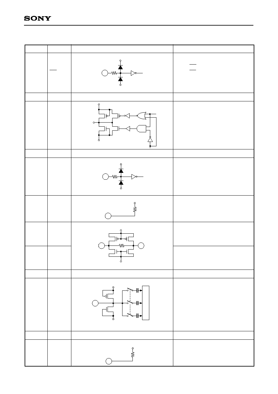
CXD1175AM/AP
No.
Symbol
Equivalent circuit
Description
1
OE
When OE = Low, Data is output.
When OE = High, D0 to D7 pins turn
to High impedance.
Digital ground
D0 (LSB) to D7 (MSB) output
Digital +5V
Clock input
DV
SS
D0 to D7
DV
DD
CLK
2, 24
3 to 10
11, 13
12
1
DV
DD
DV
SS
Di
12
DV
DD
DV
SS
17
VRT
23
VRB
14, 15, 18 AV
DD
Reference voltage (Top)
Reference voltage (Bottom)
Analog +5V
19
V
IN
20, 21
AV
SS
Analog input
Analog GND
22
VRBS
Shorted with VRB generates +0.6V.
AV
DD
AV
SS
17
23
AV
DD
AV
SS
19
AV
SS
22
Pin Description and Equivalent Circuits
AV
DD
16
16
VRTS
Shorted with VRT generates, +2.6V.

≠ 5 ≠
CXD1175AM/AP
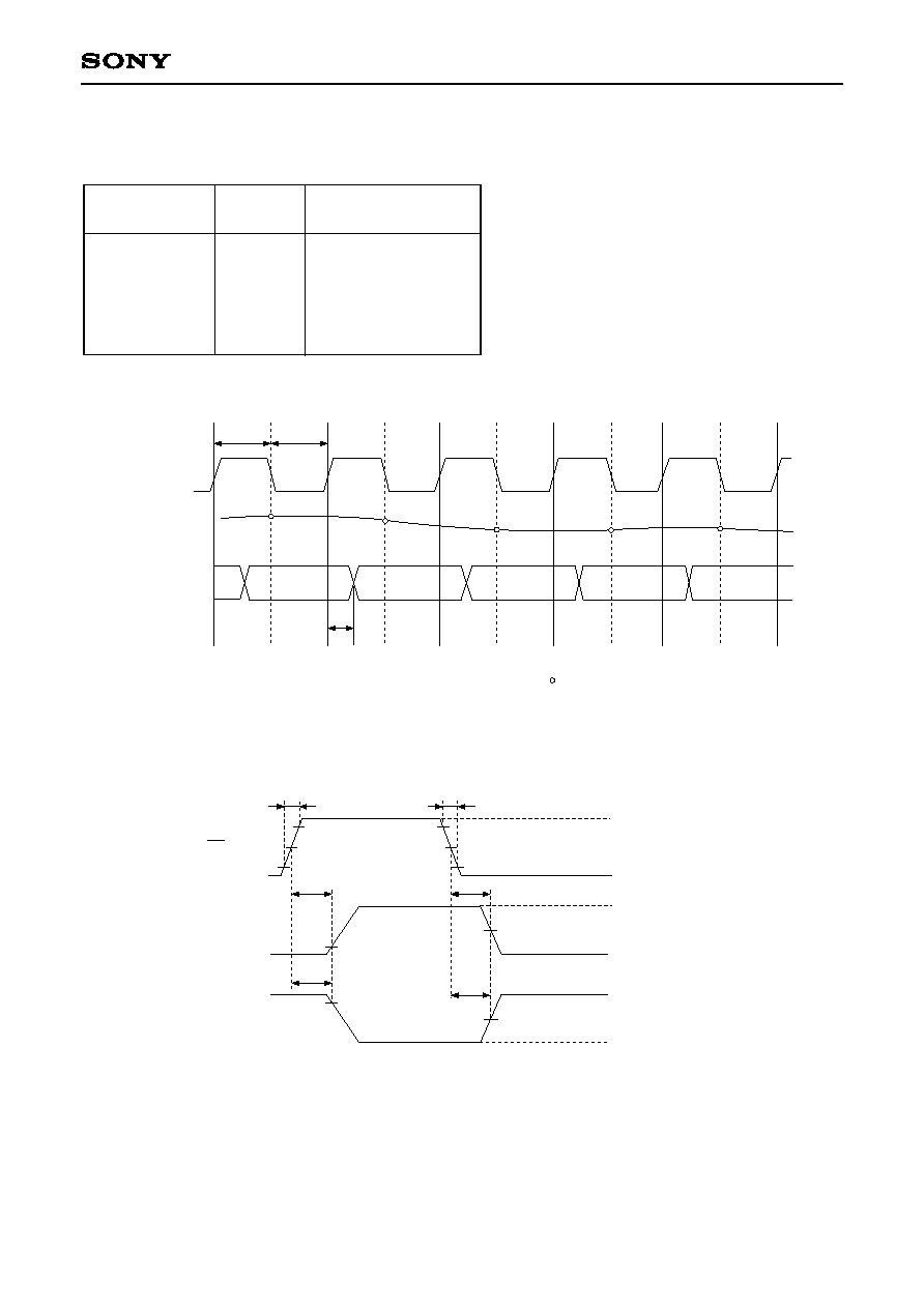
Electrical Characteristics
Analog characteristics
(Fc = 20MSPS, V
DD
= 5V, V
RB
= 0.5V, V
RT
= 2.5V, Ta = 25∞C)
Conversion speed
Analog input band width
(≠1dB)
Offset voltage
1
Integral non-linearity error
Differential non-linearity error
Differential gain error
Differential phase error
Aperture jitter
Sampling delay
Fc
BW
E
OT
E
OB
E
L
E
D
DG
DP
t
aj
t
sd
0.5
≠10
0
V
DD
= 4.75 to 5.25V
Ta = ≠40 to +85∞C
V
IN
= 0.5 to 2.5V
f
IN
= 1kHz ramp
Envelope
Potential difference to VRT
Potential difference to VRB
End point
NTSC 40 IRE mod ramp
Fc = 14.3MSPS
18
≠35
+15
+0.5
±0.3
1.0
0.5
30
4
20
≠60
+45
+1.3
±0.5
MSPS
MHz
mV
LSB
%
deg
ps
ns
Item
Symbol
Conditions
Min.
Typ.
Max.
Unit
1
The offset voltage EOB is a potential difference between VRB and a point of position where the voltage
drops equivalent to 1/2 LSB of the voltage when the output data changes from "00000000" to "00000001".
EOT is a potential difference between VRT and a potential of point where the voltage rises equivalent to
1/2LSB of the voltage when the output data changes from "11111111" to "11111110".