 | –≠–ª–µ–∫—Ç—Ä–æ–Ω–Ω—ã–π –∫–æ–º–ø–æ–Ω–µ–Ω—Ç: ICX274AQ | –°–∫–∞—á–∞—Ç—å:  PDF PDF  ZIP ZIP |
≠ 1 ≠
E01410C34
Sony reserves the right to change products and specifications without prior notice. This information does not convey any license by
any implication or otherwise under any patents or other right. Application circuits shown, if any, are typical examples illustrating the
operation of the devices. Sony cannot assume responsibility for any problems arising out of the use of these circuits.
ICX274AQ
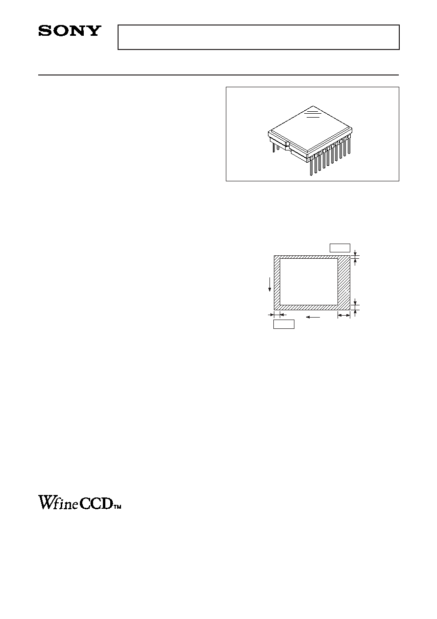
20 pin DIP (Plastic)
Description
The ICX274AQ is a diagonal 8.923mm (Type 1/1.8)
interline CCD solid-state image sensor with a square
pixel array and 2.01M effective pixels. Progressive
scan allows all pixels' signals to be output
independently within approximately 1/15 second,
and output is also possible using various addition
and pulse elimination methods. This chip features an
electronic shutter with variable charge-storage time
which makes it possible to realize full-frame still
images without a mechanical shutter. High resolution
and high color reproductivity are achieved through
the use of R, G, B primary color mosaic filters as the
color filters. Further, high sensitivity and low dark
current are achieved through the adoption of Super
HAD CCD technology.
This chip is suitable for applications such as
electronic still cameras, PC input cameras, etc.
Features
∑ High horizontal and vertical resolution
∑ Supports the following modes
Progressive scan mode (with/without mechanical shutter)
2/8-line readout mode
2/4-line readout mode
2-line addition mode
Center scan modes (1), (2) and (3)
AF modes (1) and (2)
∑ Square pixel
∑ Horizontal drive frequency: 28.6364MHz (typ.), 36.0MHz (max.)
∑ Reset gate bias are not adjusted
∑ R, G, B primary color mosaic filters on chip
∑ High sensitivity, low dark current
∑ Continuous variable-speed shutter function
∑ Excellent anti-blooming characteristics
∑ 20-pin high-precision plastic package
Device Structure
∑ Interline CCD image sensor
∑ Image size:
Diagonal 8.923mm (Type 1/1.8)
∑ Total number of pixels:
1688 (H)
◊
1248 (V) approx. 2.11M pixels
∑ Number of effective pixels: 1628 (H)
◊
1236 (V) approx. 2.01M pixels
∑ Number of active pixels:
1620 (H)
◊
1220 (V) approx. 1.98M pixels
∑ Recommended number of
recording pixels:
1600 (H)
◊
1200 (V) approx. 1.92M pixels
∑ Chip size:
8.50mm (H)
◊
6.80mm (V)
∑ Unit cell size:
4.40µm (H)
◊
4.40µm (V)
∑ Optical black:
Horizontal (H) direction: Front 12 pixels, rear 48 pixels
Vertical (V) direction:
Front 10 pixels, rear 2 pixels
∑ Number of dummy bits:
Horizontal 28
Vertical 1
∑ Substrate material:
Silicon
Optical black position
(Top View)
2
10
V
H
Pin 1
Pin 11
48
12
Wfine CCD is trademark of Sony corporation.
Represents a CCD adopting progressive scan, primary color filter and square pixel.
Diagonal 8.923mm (Type 1/1.8) Progressive Scan CCD Image Sensor with Square Pixel for Color Cameras

≠ 2 ≠
ICX274AQ
11
12
13
14
15
16
17
18
19
20
Horizontal register
Note)
V
DD
RG
H
2B
H
1B
GND
SUB
C
SUB
V
L
H
1A
H
2A
10
9
8
7
6
5
4
3
2
1
V
OUT
GND
V
1
V
2C
V
2B
V
2A
V
3C
V
3B
V
3A
V
4
B
G
B
G
B
G
R
G
R
G
B
G
B
G
B
G
R
G
R
G
G
R
G
R
B
G
G
R
B
G
G
R
V
e
r
tical register
Note) : Photo sensor
Block Diagram and Pin Configuration
(Top View)
Pin Description
1
DC bias is generated within the CCD, so that this pin should be grounded externally through a capacitance of
0.1µF.
Pin No.
Symbol
Description
Pin No.
Symbol
Description
1
2
3
4
5
6
7
8
9
10
V
4
V
3A
V
3B
V
3C
V
2A
V
2B
V
2C
V
1
GND
V
OUT
Vertical register transfer clock
Vertical register transfer clock
Vertical register transfer clock
Vertical register transfer clock
Vertical register transfer clock
Vertical register transfer clock
Vertical register transfer clock
Vertical register transfer clock
GND
Signal output
11
12
13
14
15
16
17
18
19
20
V
DD
RG
H
2B
H
1B
GND
SUB
C
SUB
V
L
H
1A
H
2A
Supply voltage
Reset gate clock
Horizontal register transfer clock
Horizontal register transfer clock
GND
Substrate clock
Substrate bias
1
Protective transistor bias
Horizontal register transfer clock
Horizontal register transfer clock

≠ 3 ≠
ICX274AQ
Absolute Maximum Ratings
2
+24V (Max.) is guaranteed when clock width < 10µs, clock duty factor < 0.1%.
+16V (Max.) is guaranteed during power-on or power-off.
Item
V
DD
, V
OUT
,
RG ≠
SUB
V
2
, V
3
≠
SUB
(
= A to C)
V
1
, V
4
, V
L
≠
SUB
H
1
, H
2
, GND ≠
SUB
(
= A, B)
C
SUB
≠
SUB
V
DD
, V
OUT
,
RG, C
SUB
≠ GND
V
1
, V
2
, V
3
, V
4
≠ GND
(
= A to C)
H
1
, H
2
≠ GND
(
= A, B)
V
2
, V
3
≠ V
L (
= A to C)
V
1
, V
4
, H
1
, H
2
, GND ≠ V
L (
= A, B)
Voltage difference between vertical clock input pins
H
1
≠ H
2
(
= A, B)
H
1
, H
2
≠ V
4 (
= A, B)
Against
SUB
Against GND
Against V
L
Between input
clock pins
Storage temperature
Guaranteed temperature of performance
Operating temperature
≠40 to +12
≠50 to +15
≠50 to +0.3
≠40 to +0.3
≠25 to
≠0.3 to +22
≠10 to +18
≠10 to +6.5
≠0.3 to +28
≠0.3 to +15
to +15
≠6.5 to +6.5
≠10 to +16
≠30 to +80
≠10 to +60
≠10 to +75
V
V
V
V
V
V
V
V
V
V
V
V
V
∞C
∞C
∞C
2
Ratings
Unit
Remarks

≠ 4 ≠
ICX274AQ
Bias Conditions
1
Progressive scan mode, 2/8-line readout mode, 2/4-line readout mode, center scan modes (1) and (3),
and AF modes (1) and (2)
2
2-line addition mode and center scan mode (2)
3
V
L
setting is the V
VL
voltage of the vertical clock waveform, or the same voltage as the V
L
power supply
for the V driver should be used.
4
Substrate voltage (V
SUB2
) setting value indication
The substrate voltage (V
SUB
) for modes without line addition is generated internally.
The substrate voltage setting value for use with vertical 2-line addition is indicated by a code on the
bottom surface of the image sensor. Adjust the substrate voltage to the indicated voltage.
V
SUB2
code ≠ 1-digit indication
V
SUB2
code
The code and the actual value correspond as follows.
[Example] "h" indicates a V
SUB2
setting of 11.6V.
5
Do not apply a DC bias to the reset gate clock pin, because a DC bias is generated within the CCD.
DC characteristics
Supply current
Item
I
DD
Symbol
10.0
Min.
Unit
Remarks
Typ.
Max.
mA
13.0
7.0
J
11.8
K
12.0
L
12.2
m
12.4
N
12.6
P
12.8
R
13.0
S
13.2
U
13.4
V
13.6
W
13.8
X
14.0
Y
14.2
Z
14.4
V
SUB2
code
Actual value
1
8.8
2
9.0
3
9.2
4
9.4
6
9.6
7
9.8
8
10.0
9
10.2
A
10.4
C
10.6
d
10.8
E
11.0
f
11.2
G
11.4
h
11.6
V
SUB2
code
Actual value
Supply voltage
Protective transistor bias
Substrate voltage
adjustment range
Substrate voltage adjustment accuracy
Reset gate clock
Item
V
DD
V
L
V
SUB
V
SUB2
V
SUB
RG
Symbol
15.0
3
Internally generated value
Indicated
voltage
5
Min.
V
V
V
V
Unit
4
Remarks
Typ.
Max.
No line addition
1
2-line addition
2
14.55
8.8
Indicated
voltage ≠ 0.2
15.45
14.4
Indicated
voltage + 0.2

≠ 5 ≠
ICX274AQ
Clock Voltage Conditions
Readout clock
voltage
Vertical transfer
clock voltage
Horizontal transfer
clock voltage
Reset gate clock
voltage
Substrate clock
voltage
Item
V
VT
V
VH1
, V
VH2
V
VH3
, V
VH4
V
VL1
, V
VL2
,
V
VL3
, V
VL4
V
V
V
VH3
≠ V
VH
V
VH4
≠ V
VH
V
VHH
V
VHL
V
VLH
V
VLL
V
H
V
HL
V
CR
V
RG
V
RGLH
≠ V
RGLL
V
RGL
≠ V
RGLm
V
SUB
Symbol
14.55
≠0.05
≠0.2
≠8.0
6.8
≠0.25
≠0.25
4.75
≠0.05
0.8
3.0
21.5
Min.
15.0
0
0
≠7.5
7.5
5.0
0
2.5
3.3
22.5
Typ.
15.45
0.05
0.05
≠7.0
8.05
0.1
0.1
0.5
0.5
0.5
0.5
5.25
0.05
5.25
0.4
0.5
23.5
Max.
Unit
1
2
2
2
2
2
2
2
2
2
2
3
3
3
4
4
4
5
Waveform
diagram
V
VH
= (V
VH1
+ V
VH2
)/2
V
VL
= (V
VL3
+ V
VL4
)/2
V
V
= V
VH
n ≠ V
VL
n (n = 1 to 4)
High-level coupling
High-level coupling
Low-level coupling
Low-level coupling
Cross-point voltage
Low-level coupling
Low-level coupling
Remarks
V
V
V
V
V
V
V
V
V
V
V
V
V
V
V
V
V
V