≠ 1 ≠
E01318-PS
Sony reserves the right to change products and specifications without prior notice. This information does not convey any license by
any implication or otherwise under any patents or other right. Application circuits shown, if any, are typical examples illustrating the
operation of the devices. Sony cannot assume responsibility for any problems arising out of the use of these circuits.
CXD3607R
48 pin LQFP (Plastic)
Timing Generator for Progressive Scan CCD Image Sensor
Description
The CXD3607R is a timing generator IC which
generates the timing pulses required by Progressive
Scan CCD image sensors as well as signal processing
circuits.
Features
∑ Base oscillation frequency 57.3MHz
∑ High-speed/low-speed shutter function
∑ Supports FINE and DRAFT mode drive
(15 frames/s, 60 frames/s possible)
∑ Random trigger shutter function
(Supports TRIG and TRIGOUT mode drive)
∑ Horizontal driver for CCD image sensor
∑ Vertical driver for CCD image sensor
Applications
Progressive scan CCD cameras
Structure
Silicon gate CMOS IC
Applicable CCD Image Sensors
ICX285 (Type 2/3, 1450K pixels)
Absolute Maximum Ratings
∑ Supply voltage
V
DD
a, b
Vss ≠ 0.3 to +7.0
V
V
L
≠10.0 to Vss
V
V
H
V
L
≠ 0.3 to +26.0
V
∑ Input voltage
V
I
Vss ≠ 0.3 to V
DD
+ 0.3 V
∑ Output voltage
V
O1
Vss ≠ 0.3 to V
DD
+ 0.3 V
V
O2
V
L
≠ 0.3 to Vss + 0.3
V
V
O3
V
L
≠ 0.3 to V
H
+ 0.3
V
∑ Operating temperature
Topr
≠20 to +75
∞C
∑ Storage temperature
Tstg
≠55 to +150
∞C
Recommended Operating Conditions
∑ Supply voltage
V
DD
a
4.75 to 5.25
V
V
DD
b
3.0 to 3.6
V
V
M
0.0
V
V
H
14.55 to 15.45
V
V
L
≠7.5 to ≠6.5
V
∑ Operating temperature
Topr
≠20 to +75
∞C
≠ 4 ≠
CXD3607R
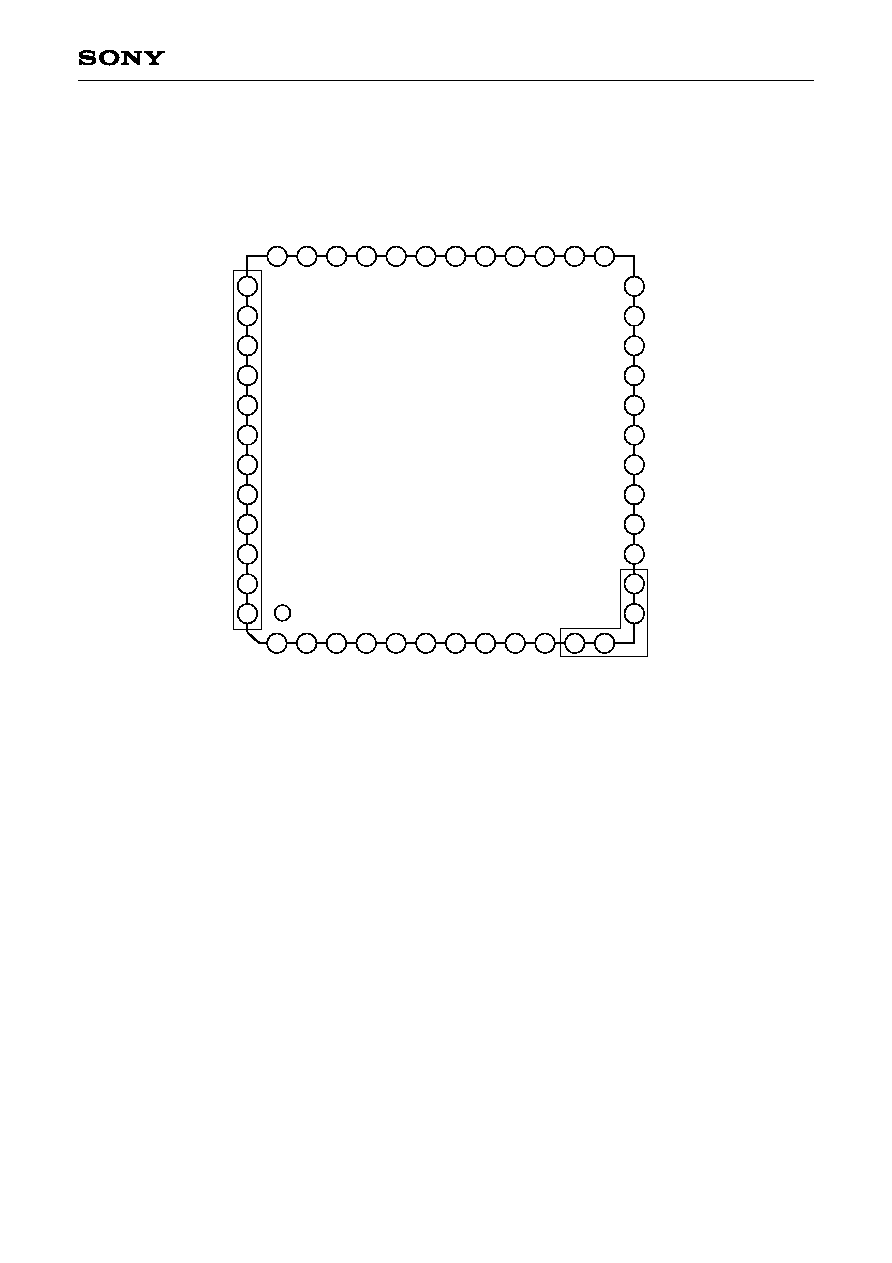
Pin Description
Pin
No.
Symbol
I/O
Description
1
2
3
4
5
6
7
8
9
10
11
12
13
14
15
16
17
18
19
20
21
22
23
24
25
26
27
28
29
30
31
32
33
34
35
V
SS
4
RST
SYNSL
NC
NC
NC
V
DD
4
TEST1
TEST2
RG
V
SS
1
H1
H2
V
DD
1
V
DD
2
XSHD
XSHP
XCPDM
XCPOB
PBLK
ADCLK
MCKO
CKO
V
SS
2
CKI
OSCO
OSCI
V
DD
3
SSI
SCK
SEN
VD
HD
TRIG
WEN
--
I
I
--
--
--
--
I
I
O
--
O
O
--
--
O
O
O
O
O
O
O
O
--
I
O
I
--
I
I
I
I
I
I
O
GND (GND for common logic block)
Internal system reset input. (High: Normal operation, Low: Reset operation)
Normally apply reset during power-on.
Control input used to switch sync system. (High: CKI sync, Low: MCKO sync)
With pull-down resistor
(Leave open.)
(Leave open.)
(Leave open.)
3.3V power supply. (Power supply for common logic block)
IC test pin 1 (Normally fix to GND.)
IC test pin 2 (Normally fix to GND.)
With pull-down resistor
CCD reset gate pulse output.
GND (GND for H1 and H2 pins)
Horizontal CCD drive clock output.
Horizontal CCD drive clock output.
5.0V power supply. (Power supply for H1 and H2 pins)
3.3V power supply. (Power supply for common logic block)
CCD data level sample-and-hold pulse output.
CCD precharge level sample-and-hold pulse output.
CCD dummy signal clamp pulse output.
CCD optical black signal clamp pulse output.
Pulse output for horizontal and vertical blanking period pulse cleaning.
Clock output for analog/digital conversion IC.
System clock output for signal processing IC. (28.6MHz)
Inverter output. (57.3MHz)
GND (GND for common logic block)
Inverter input. (57.3MHz)
Inverter output for oscillation. (57.3MHz)
Inverter input for oscillation. (57.3MHz)
3.3V power supply. (Power supply for common logic block)
Serial interface data input for internal mode settings.
Serial interface clock input for internal mode settings.
Serial interface strobe input for internal mode settings.
Vertical sync signal input.
Horizontal sync signal input.
Trigger pulse input.
Memory write timing pulse output.
≠ 5 ≠
CXD3607R
Pin
No.
Symbol
I/O
Description
36
37
38
39
40
41
42
43
44
45
46
47
48
V
SS
3
V
M
V1
V4
V2A
V
H
V2B
NC
NC
V
L
NC
V3
SUB
--
--
O
O
O
--
O
--
--
--
--
O
O
GND (GND for common logic block)
GND (GND for vertical driver)
CCD vertical register clock output.
CCD vertical register clock output.
CCD vertical register clock output.
15.0V power supply. (Power supply for vertical driver)
CCD vertical register clock output.
(Leave open.)
(Leave open.)
≠7.0V power supply. (Power supply for vertical driver)
(Leave open.)
CCD vertical register clock output.
CCD electronic shutter pulse output.