
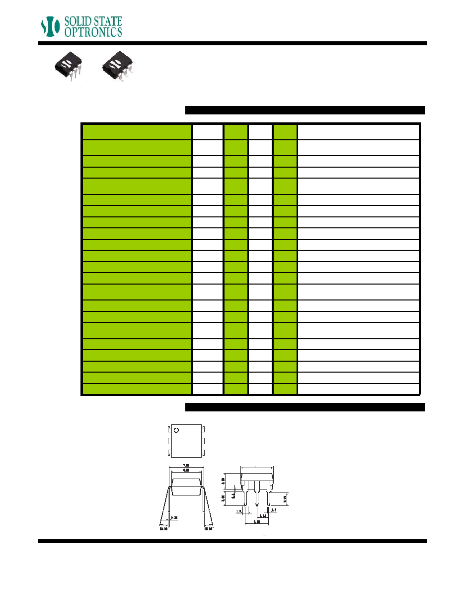
SDT600
DC Input
Optocoupler
The SDT600 consists of a phototransistor optically coupled to a light emitting diode. Optical coupling between the input LED and output
phototransistor allows for high isolation levels while maintaining low-level DC signal control capability. The SDT600 provides an optically
isolated method of controlling many interface applications such as telecommunications, industrial control and instrumentation circuitry.
DESCRIPTION
FEATURES
APPLICATIONS
OPTIONS/SUFFIXES
SCHEMATIC DIAGRAM
MAXIMUM RATINGS
APPROVALS
High input-to-output isolation package (5000 Vrms)
Low input power consumption
High stability
6 Pin DIP Package
with Base Connection
Loop current detection
Ring signal detection
Power supply feedback isolation
Audio signal interface
Transformer replacement
Digital logic inputs
Microprocessor inputs
Surface Mount Option
-S
Tape and Reel Option
-TR
PARAMETER
UNIT
MIN
TYP
MAX
Storage Temperature
∞C
-55
125
Operating Temperature
∞C
-40
100
Continuous Input Current
mA
50
Transient Input Current
A
1
Reverse Input Control
Voltage
V
6
Total Power Dissipation
mW
200
UL and C-UL approved File # E201932
rev 1.0
Solid State Optronics, Inc.
1.888.377.4776
www.ssousa.com
1. Anode
2. Cathode
3. NC
4. Emitter
5. Collector
6. Base
SDT600
DC Input
Optocoupler
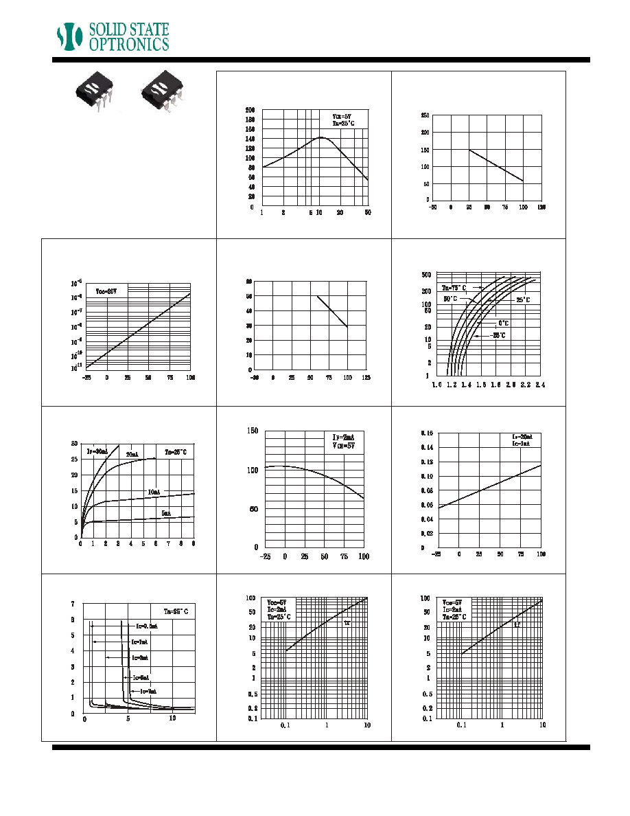
ELECTRICAL CHARACTERISTICS - 25∞
PARAMETER
UNIT
MIN
TYP
MAX TEST CONDITIONS
INPUT SPECIFICATIONS
Forward Voltage
V
1.2
1.4
If = 20mA
Reverse Current
10
Vr = 4V
A
OUTPUT SPECIFICATIONS
Collector-Emitter Breakdown Voltage
V
Ic = 10uA
Emitter-Collector Breakdown Voltage
V
Ie = 10uA
Dark Current
0.1
Vce = 20V
A
Floating Capacitance
p
0.6
1
V = 0V, f=1.0MHz
F
Saturation Voltage
V
0.1
0.3
If = 20mA, Ic = 1mA
Current Transfer Ratio
%
60
600
If = 2mA, Vce = 5V
Rise Time
5
Ic = 2mA, Vc
e = 5V, Rc = 100 ohms
s
Fall Time
4
Ic = 2mA, Vc
e = 5V, Rc = 100 ohms
s
COUPLED SPECIFICATIONS
Isolation Voltage
V
5000
T = 1 minute
Isolation Resistance
G
50
CTR CLASSIFICATION
-A
%
60
160
-B
%
130
260
-C
%
200
400
-D
%
300
600
-E
%
60
600
rev 1.0
Solid State Optronics, Inc.
1.888.377.4776
www.ssousa.com
60
6
TOLERANCE :+ 0.25mm
Unit
(mm)
MECHANICAL DIMENSIONS
rev 1.0
Solid State Optronics, Inc.
1.888.377.4776
www.ssousa.com
SDT600
Fig.1 Current Transfer Ratio vs.
Forward Current
Forward Current I
F
(mA)
Current transfer ratio CTR (%)
Fig.2 Collector Power Dissipation vs.
Ambient Temperature
Ambient Temperature Ta (∞C)
Collector Power Dissipation Pc (mW)
Fig.4 Forward Current vs. Ambient
Temperature
Ambient Temperature Ta (∞C)
Forward Current I
F
(mA)
Fig.5 Forward Current vs. Forward
Voltage
Forward Voltage V
F
(V)
Forward Current I
F
(mA)
Fig.7 Relative Current Transfer Ratio
vs. Ambient Temperature
Ambient Temperature Ta (∞C)
Relative Current T
ransfer Ratio (%)
Fig.8 Collector-emitter Saturation
Voltage vs. Ambient Temperature
Ambient Temperature Ta (∞C)
Collector-emitter Saturation V
oltage Vce (V)
Fig.10 Response Time vs. Load
Resistance
Load Resistance R
L
(Kohm)
Response Rise T
ime (us)
Fig.3 Collector Dark Current vs.
Ambient Temperature
Ambient Temperature Ta (∞C)
Collector Dark Current Iceo (A)
Fig.6 Collector Current vs. Collector-
emitter Voltage
Collector-emitter Voltage V
CE
(V)
Collector Current Ic (mA)
Fig.9 Collector-emitter Saturation
Voltage vs. Forward Current
Forward Current I
F
(mA)
Collector-emitter Saturation V
oltage Vce (V)
Fig.11 Response Time vs. Load
Resistance
Load Resistance R
L
(Kohm)
Response Rise T
ime (us)