©2001 Silicon Storage Technology, Inc.
S71107-03-000
5/01
349
1
The SST logo and SuperFlash are registered trademarks of Silicon Storage Technology, Inc.
ComboMemory are trademarks of Silicon Storage Technology, Inc.
These specifications are subject to change without notice.
Data Sheet
FEATURES:
∑
Monolithic Flash + SRAM ComboMemory
≠ SST31LF041/041A: 512K x8 Flash + 128K x8 SRAM
≠ SST31LF043/043A: 512K x8 Flash + 32K x8 SRAM
∑
Single 3.0-3.6V Read and Write Operations
∑
Concurrent Operation
≠ Read from or write to SRAM while
Erase/Program Flash
∑
Superior Reliability
≠ Endurance: 100,000 Cycles (typical)
≠ Greater than 100 years Data Retention
∑
Low Power Consumption:
≠ Active Current: 10 mA (typical) for Flash and
20 mA (typical) for SRAM Read
≠ Standby Current: 10 µA (typical)
∑
Flash Sector-Erase Capability
≠ Uniform 4 KByte sectors
∑
Latched Address and Data for Flash
∑
Fast Read Access Times:
≠ SST31LF041/043
Flash: 70 ns
SRAM: 70 ns
≠ SST31LF041A/043A
Flash: 300 ns
SRAM: 300 ns
∑
Flash Fast Erase and Byte-Program:
≠ Sector-Erase Time: 18 ms (typical)
≠ Bank-Erase Time: 70 ms (typical)
≠ Byte-Program Time: 14 µs (typical)
≠ Bank Rewrite Time: 8 seconds (typical)
∑
Flash Automatic Erase and Program Timing
≠ Internal V
PP
Generation
∑
Flash End-of-Write Detection
≠ Toggle Bit
≠ Data# Polling
∑
CMOS I/O Compatibility
∑
JEDEC Standard Command Set
∑
Packages Available
≠ 32-lead TSOP (8 x 14 mm) SST31LF041A/043A
≠ 40-lead TSOP (10 x 14 mm) SST31LF041/043
PRODUCT DESCRIPTION
The SST31LF041/041A/043/043A devices are a 512K x8
CMOS flash memory bank combined with a 128K x8 or
32K x8 CMOS SRAM memory bank manufactured with
SST's proprietary, high performance SuperFlash technol-
ogy. The SST31LF041/041A/043/043A devices write
(SRAM or flash) with a 3.0-3.6V power supply. The mono-
lithic SST31LF041/041A/043/043A devices conform to
Software Data Protect (SDP) commands for x8
EEPROMs.
Featuring high performance Byte-Program, the flash mem-
ory bank provides a maximum Byte-Program time of 20
µsec. The entire flash memory bank can be erased and
programmed byte-by-byte in typically 8 seconds, when
using interface features such as Toggle Bit or Data# Polling
to indicate the completion of Program operation. To protect
against inadvertent flash write, the SST31LF041/041A/
043/043A devices have on-chip hardware and Software
Data Protection schemes. Designed, manufactured, and
tested for a wide spectrum of applications, the
SST31LF041/041A/043/043A devices are offered with a
guaranteed endurance of 10,000 cycles. Data retention is
rated at greater than 100 years.
The SST31LF041/041A/043/043A operate as two inde-
pendent memory banks with respective bank enable sig-
nals. The SRAM and Flash memory banks are
superimposed in the same memory address space. Both
memory banks share common address lines, data lines,
WE# and OE#. The memory bank selection is done by
memory bank enable signals. The SRAM bank enable sig-
nal, BES# selects the SRAM bank and the flash memory
bank enable signal, BEF# selects the flash memory bank.
The WE# signal has to be used with Software Data Protec-
tion (SDP) command sequence when controlling the Erase
and Program operations in the flash memory bank. The
SDP command sequence protects the data stored in the
flash memory bank from accidental alteration.
The SST31LF041/041A/043/043A provide the added func-
tionality of being able to simultaneously read from or write
to the SRAM bank while erasing or programming in the
flash memory bank. The SRAM memory bank can be read
or written while the flash memory bank performs Sector-
Erase, Bank-Erase, or Byte-Program concurrently. All flash
memory Erase and Program operations will automatically
latch the input address and data signals and complete the
operation in background without further input stimulus
requirement. Once the internally controlled Erase or Pro-
gram cycle in the flash bank has commenced, the SRAM
bank can be accessed for Read or Write.
The SST31LF041/041A/043/043A devices are suited for
applications that use both nonvolatile flash memory and
volatile SRAM memory to store code or data. For all sys-
tem applications, the SST31LF041/041A/043/043A
4 Mbit Flash + 1 Mbit or 256 Kbit SRAM ComboMemory
SST31LF041 / SST31LF041A / SST31LF043 / SST31LF043A
SST31LF041 / 041A4Mb Flash (x8) + 1 Mb SRAM (x8) ComboMemories
2
Data Sheet
4 Mbit Flash + 1 Mbit or 256 Kbit SRAM ComboMemory
SST31LF041 / SST31LF041A / SST31LF043 / SST31LF043A
©2001 Silicon Storage Technology, Inc.
S71107-03-000
5/01
349
devices significantly improve performance and reliability,
while lowering power consumption, when compared with
multiple chip solutions. The SST31LF041/041A/043/043A
inherently use less energy during Erase and Program than
alternative flash technologies. When programming a flash
device, the total energy consumed is a function of the
applied voltage, current, and time of application. Since for
any given voltage range, the SuperFlash technology uses
less current to program and has a shorter Erase time, the
total energy consumed during any Erase or Program oper-
ation is less than alternative flash technologies. The mono-
lithic ComboMemory eliminates redundant functions when
using two separate memories of similar architecture; there-
fore, reducing the total power consumption.
The SuperFlash technology provides fixed Erase and Pro-
gram times, independent of the number of Erase/Program
cycles that have occurred. Therefore the system software
or hardware does not have to be modified or de-rated as is
necessary with alternative flash technologies, whose Erase
and Program times increase with accumulated Erase/Pro-
gram cycles.
The SST31LF041/041A/043/043A devices also improve
flexibility by using a single package and a common set of
signals to perform functions previously requiring two sepa-
rate devices. To meet high density, surface mount require-
ments, the SST31LF041/043 device is offered in 40-lead
TSOP package and the SST31LF041A/043A device is
offered in 32-lead TSOP package. See Figures 1 and 2 for
the pinouts.
Device Operation
The ComboMemory uses BES# and BEF# to control oper-
ation of either the SRAM or the flash memory bank. Bus
contention is eliminated as the monolithic device will not
recognize both bank enables as being simultaneously
active. If both bank enables are asserted (i.e., BEF# and
BES# are both low), the BEF# will dominate while the
BES# is ignored and the appropriate operation will be exe-
cuted in the flash memory bank. SST does not recommend
that both bank enables be simultaneously asserted. All
other address, data, and control lines are shared which
minimizes power consumption and area. The device goes
into standby when both bank enables are raised to V
IHC
.
See Table 3 for SRAM operation mode selection.
For SST31LF041A/043A only: BES# and OE# share
pin 32. During SRAM operation, pin 32 will function as
BES#. During flash operation, pin 32 will function as OE#.
When pin 32 (OE#/BES#) is high, the data bus is in high
impedance state.
SRAM Operation
With BES# low and BEF# high, the SST31LF041/041A
operate as a 128K x8 CMOS SRAM and the
SST31LF043/043A operate as 32K x8 CMOS SRAM, with
fully static operation requiring no external clocks or timing
strobes. The SRAM is mapped into the first 128 KByte
address space of the device for 041/041A or 32 KByte for
043/043A. Read and Write cycle times are equal.
SRAM Read
The SRAM Read operation of the SST31LF041/041A/
043/043A are controlled by OE# and BES#, both have to
be low with WE# high, for the system to obtain data from
the outputs. BES# is used for SRAM bank selection.
When BES# and BEF# are high, both memory banks are
deselected. OE# is the output control and is used to gate
data from the output pins. The data bus is in high imped-
ance state when OE# is high. See Figure 3 for the Read
cycle timing diagram.
SRAM Write
The SRAM Write operation of the SST31LF041/041A/043/
043A is controlled by WE# and BES#; both have to be low
for the system to write to the SRAM. BES# is used for
SRAM bank selection. During the Byte-Write operation, the
addresses and data are referenced to the rising edge of
either BES# or WE#, whichever occurs first. The Write time
is measured from the last falling edge to the first rising edge
of BES# and WE#. OE# can be V
IL
or V
IH
, but no other
value, for SRAM Write operations. See Figure 4 for the
SRAM Write cycle timing diagram.
Flash Operation
With BEF# active, the SST31LF041/041A/043/043A oper-
ate as a 512K x8 flash memory. The flash memory bank is
read using the common address lines, data lines, WE# and
OE#. Erase and Program operations are initiated with the
JEDEC standard SDP command sequences. Address and
data are latched during the SDP commands and internally
timed Erase and Program operations. See Table 3 for flash
operation mode selection.
Flash Read
The Read operation of the SST31LF041/041A/043/043A
devices are controlled by BEF# and OE#; both have to be
low, with WE# high, for the system to obtain data from the
outputs. BEF# is used for flash memory bank selection.
When BEF# and BES# are high, both banks are dese-
lected and only standby power is consumed. OE# is the
Data Sheet
4 Mbit Flash + 1 Mbit or 256 Kbit SRAM ComboMemory
SST31LF041 / SST31LF041A / SST31LF043 / SST31LF043A
3
©2001 Silicon Storage Technology, Inc.
S71107-03-000
5/01
349
output control and is used to gate data from the output pins.
The data bus is in high impedance state when OE# is high.
See Figure 5 for the Read cycle timing diagram.
Flash Erase/Program Operation
SDP commands are used to initiate the flash memory bank
Program and Erase operations of the SST31LF041/041A/
043/043A. SDP commands are loaded to the flash mem-
ory bank using standard microprocessor write sequences.
A command is loaded by asserting WE# low while keeping
BEF# low and OE# high. The address is latched on the fall-
ing edge of WE# or BEF#, whichever occurs last. The data
is latched on the rising edge of WE# or BEF#, whichever
occurs first.
Flash Byte-Program Operation
The flash memory bank of the SST31LF041/041A/043/
043A devices are programmed on a byte-by-byte basis.
Before the Program operations, the memory must be
erased first. The Program operation consists of three steps.
The first step is the three-byte-load sequence for Software
Data Protection. The second step is to load byte address
and byte data. During the Byte-Program operation, the
addresses are latched on the falling edge of either BEF# or
WE#, whichever occurs last. The data is latched on the ris-
ing edge of either BEF# or WE#, whichever occurs first.
The third step is the internal Program operation which is ini-
tiated after the rising edge of the fourth WE# or BEF#,
whichever occurs first. The Program operation, once initi-
ated, will be completed, within 20 µs. See Figures 6 and 7
for WE# and BEF# controlled Program operation timing
diagrams and Figure 17 for flowcharts. During the Program
operation, the only valid Flash Read operations are Data#
Polling and Toggle Bit. During the internal Program opera-
tion, the host is free to perform additional tasks. Any SDP
commands loaded during the internal Program operation
will be ignored.
Flash Sector-Erase Operation
The Sector-Erase operation allows the system to erase the
flash memory bank on a sector-by-sector basis. The sector
architecture is based on uniform sector size of 4 KBytes.
The Sector-Erase operation is initiated by executing a six-
byte-command load sequence for Software Data Protec-
tion with Sector-Erase command (30H) and sector address
(SA) in the last bus cycle. The address lines A
18
-A
12
will be
used to determine the sector address. The sector address
is latched on the falling edge of the sixth WE# pulse, while
the command (30H) is latched on the rising edge of the
sixth WE# pulse. The internal Erase operation begins after
the sixth WE# pulse. The End-of-Erase can be determined
using either Data# Polling or Toggle Bit methods. See Fig-
ure 10 for timing waveforms. Any SDP commands loaded
during the Sector-Erase operation will be ignored.
Flash Bank-Erase Operation
The SST31LF041/041A/043/043A flash memory bank pro-
vides a Bank-Erase operation, which allows the user to
erase the entire flash memory bank array to the "1s" state.
This is useful when the entire bank must be quickly erased.
The Bank-Erase operation is initiated by executing a six-
byte Software Data Protection command sequence with
Bank-Erase command (10H) with address 5555H in the last
byte sequence. The internal Erase operation begins with
the rising edge of the sixth WE# or BEF# pulse, whichever
occurs first. During the internal Erase operation, the only
valid Flash Read operations are Toggle Bit and Data# Poll-
ing. See Table 4 for the command sequence, Figure 11 for
timing diagram, and Figure 20 for the flowchart. Any SDP
commands loaded during the Bank-Erase operation will be
ignored.
Flash Write Operation Status Detection
The SST31LF041/041A/043/043A flash memory bank pro-
vides two software means to detect the completion of a
flash memory bank Write (Program or Erase) cycle, in
order to optimize the system Write cycle time. The software
detection includes two status bits: Data# Polling (DQ
7
) and
Toggle Bit (DQ
6
). The End-of-Write detection mode is
enabled after the rising edge of WE#, which initiates the
internal Program or Erase operation. The actual comple-
tion of the nonvolatile write is asynchronous with the sys-
tem; therefore, either a Data# Polling or Toggle Bit Read
may be simultaneous with the completion of the Write
cycle. If this occurs, the system may possibly get an errone-
ous result, i.e., valid data may appear to conflict with either
DQ
7
or DQ
6
. In order to prevent spurious rejection, if an
erroneous result occurs, the software routine should
include a loop to read the accessed location an additional
two (2) times. If both reads are valid, then the device has
completed the Write cycle, otherwise the rejection is valid.
Flash Data# Polling (DQ
7
)
When the SST31LF041/041A/043/043A flash memory
bank is in the internal Program operation, any attempt to
read DQ
7
will produce the complement of the true data.
Once the Program operation is completed, DQ
7
will pro-
duce true data. The flash memory bank is then ready for
the next operation. During internal Erase operation, any
attempt to read DQ
7
will produce a `0'. Once the internal
Erase operation is completed, DQ
7
will produce a `1'. The
Data# Polling is valid after the rising edge of the fourth WE#
4
Data Sheet
4 Mbit Flash + 1 Mbit or 256 Kbit SRAM ComboMemory
SST31LF041 / SST31LF041A / SST31LF043 / SST31LF043A
©2001 Silicon Storage Technology, Inc.
S71107-03-000
5/01
349
(or BEF#) pulse for Program operation. For Sector or Bank-
Erase, the Data# Polling is valid after the rising edge of the
sixth WE# (or BEF#) pulse. See Figure 8 for Data# Polling
timing diagram and Figure 18 for a flowchart.
Flash Toggle Bit (DQ
6
)
During the internal Program or Erase operation, any con-
secutive attempts to read DQ
6
will produce alternating 0s
and 1s, i.e., toggling between 0 and 1. When the internal
Program or Erase operation is completed, the toggling will
stop. The flash memory bank is then ready for the next
operation. The Toggle Bit is valid after the rising edge of the
fourth WE# (or BE#) pulse for Program operation. For Sec-
tor or Bank-Erase, the Toggle Bit is valid after the rising
edge of the sixth WE# (or BEF#) pulse. See Figure 9 for
Toggle Bit timing diagram and Figure 18 for a flowchart.
Flash Memory Data Protection
The SST31LF041/041A/043/043A flash memory bank pro-
vides both hardware and software features to protect non-
volatile data from inadvertent writes.
Flash Hardware Data Protection
Noise/Glitch Protection: A WE# or BEF# pulse of less than
5 ns will not initiate a Write cycle.
V
DD
Power Up/Down Detection: The Write operation is
inhibited when is less than 1.5V.
Write Inhibit Mode: Forcing OE# low, BEF# high, or WE#
high will inhibit the Flash Write operation. This prevents
inadvertent writes during power-up or power-down.
Flash Software Data Protection (SDP)
The SST31LF041/041A/043/043A provide the JEDEC
approved Software Data Protection scheme for all flash
memory bank data alteration operations, i.e., Program and
Erase. Any Program operation requires the inclusion of a
series of three-byte sequence. The three byte-load
sequence is used to initiate the Program operation, provid-
ing optimal protection from inadvertent Write operations,
e.g., during the system power-up or power-down. Any
Erase operation requires the inclusion of six-byte load
sequence. The SST31LF041/041A/043/043A devices are
shipped with the Software Data Protection permanently
enabled. See Table 4 for the specific software command
codes. During SDP command sequence, invalid SDP com-
mands will abort the device to the Read mode, within T
RC
.
Concurrent Read and Write Operations
The SST31LF041/041A/043/043A provide the unique ben-
efit of being able to read from or write to SRAM, while
simultaneously erasing or programming the Flash. The
device will ignore all SDP commands when an Erase or
Program operation is in progress. This allows data alter-
ation code to be executed from SRAM, while altering the
data in Flash. The following table lists all valid states. SST
does not recommend that both bank enables, BEF# and
BES#, be simultaneously asserted.
Note that Product Identification commands use SDP;
therefore, these commands will also be ignored while an
Erase or Program operation is in progress.
Product Identification
The product identification mode identifies the devices as
either SST31LF041/043 or SST31LF041A/043A and the
manufacturer as SST. This mode may be accessed by
hardware or software operations. The hardware device ID
Read operation is typically used by a programmer to iden-
tify the correct algorithm for the SST31LF041/041A/043/
043A flash memory banks. Users may wish to use the soft-
ware product identification operation to identify the part
(i.e., using the device ID) when using multiple manufactur-
ers in the same socket. For details, see Table 3 for hard-
ware operation or Table 4 for software operation, Figure 12
for the software ID entry and read timing diagram and Fig-
ure 19 for the ID entry command sequence flowchart.
Product Identification Mode Exit/Reset
In order to return to the standard Read mode, the Software
Product Identification mode must be exited. Exiting is
accomplished by issuing the Exit ID command sequence,
C
ONCURRENT
R
EAD
/W
RITE
S
TATE
T
ABLE
Flash
SRAM
Program/Erase
Read
Program/Erase
Write
TABLE
1: P
RODUCT
I
DENTIFICATION
Address
Data
Manufacturer's ID
0000H
BFH
Device ID
SST31LF041
0001H
17H
SST31LF041A
0001H
16H
SST31LF043
0001H
65H
SST31LF043A
0001H
66H
T1.2 349
Data Sheet
4 Mbit Flash + 1 Mbit or 256 Kbit SRAM ComboMemory
SST31LF041 / SST31LF041A / SST31LF043 / SST31LF043A
5
©2001 Silicon Storage Technology, Inc.
S71107-03-000
5/01
349
which returns the device to the Read operation. Please
note that the software-reset command is ignored during an
internal Program or Erase operation. See Table 4 for soft-
ware command codes, Figure 13 for timing waveform and
Figure 19 for a flowchart.
Design Considerations
SST recommends a high frequency 0.1 µF ceramic capac-
itor to be placed as close as possible between V
DD
and
V
SS
, e.g., less than 1 cm away from the V
DD
pin of the
device. Additionally, a low frequency 4.7 µF electrolytic
capacitor from V
DD
to V
SS
should be placed within 1 cm of
the V
DD
pin.
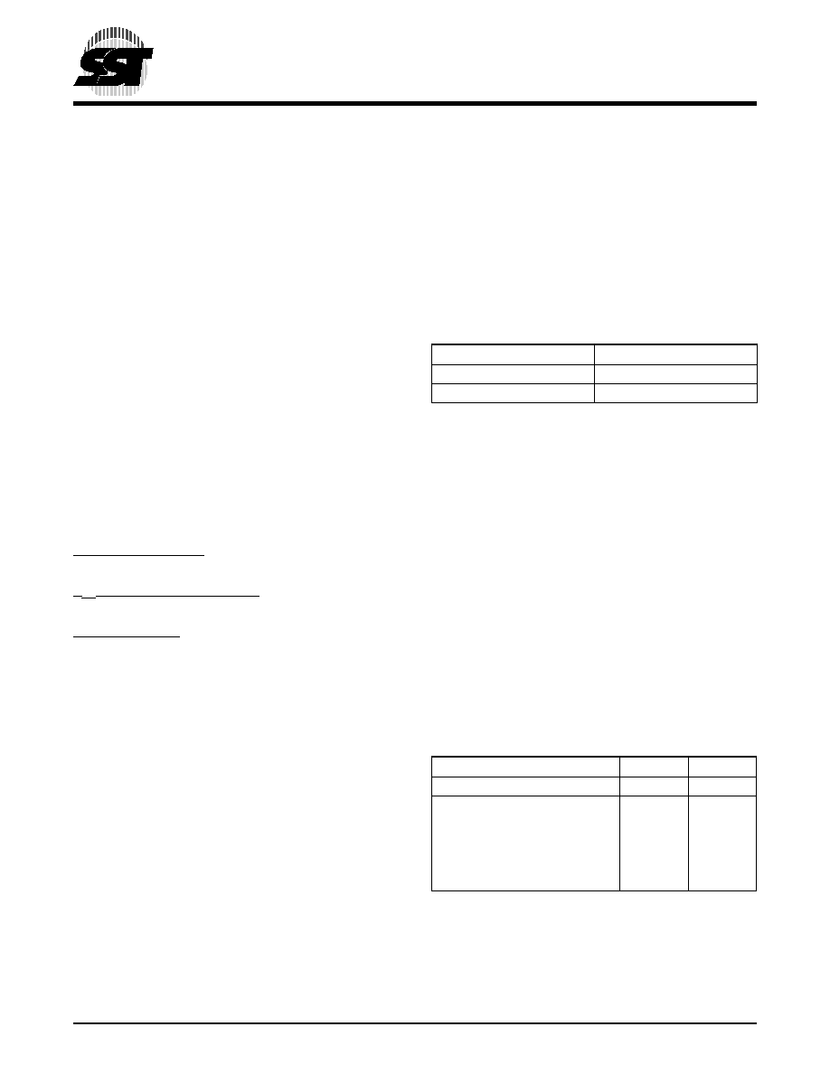
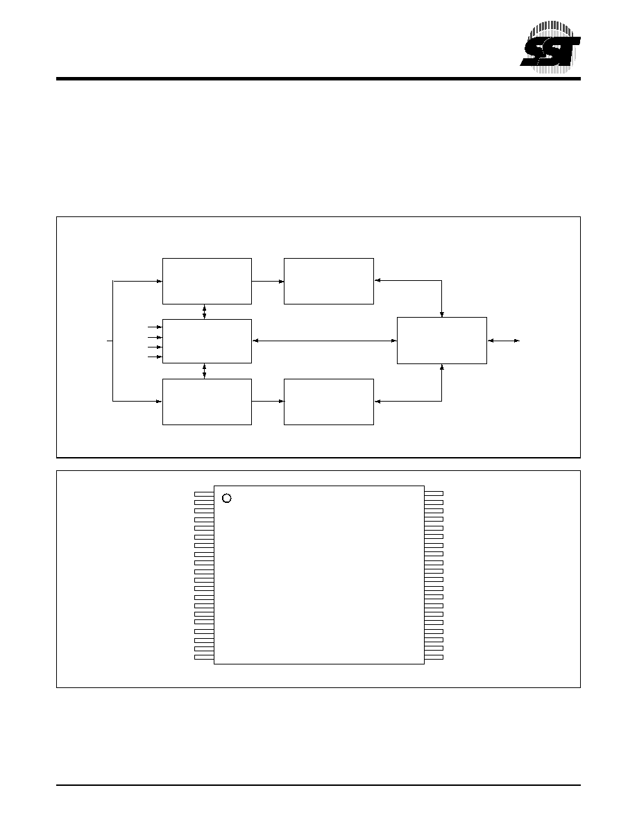
FIGURE 1: P
IN
A
SSIGNMENTS
FOR
40-
LEAD
TSOP (10
MM
X
14
MM
) - SSTLF041/043
I/O Buffers
349 ILL B1.6
Address Buffers
DQ7 - DQ0
OE#
BEF#
WE#
SuperFlash
Memory
SRAM
Control Logic
BES#
AMS - A0
AMS = Most Significant Address
Address Buffers
& Latches
F
UNCTIONAL
B
LOCK
D
IAGRAM
A16
A15
A14
A13
A12
A11
A9
A8
WE#
NC
BES#
NC
A18
A7
A6
A5
A4
A3
A2
A1
1
2
3
4
5
6
7
8
9
10
11
12
13
14
15
16
17
18
19
20
A17
VSS
NC
NC
A10
DQ7
DQ6
DQ5
DQ4
VDD
VDD
NC
DQ3
DQ2
DQ1
DQ0
OE#
VSS
BEF#
A0
40
39
38
37
36
35
34
33
32
31
30
29
28
27
26
25
24
23
22
21
349 ILL F01.2
Standard Pinout
Top View
Die Up