74ACT16244
16-BIT BUS BUFFER
WITH 3 STATE OUTPUTS (NON INVERTED)
Æ
February 2000
s
HIGH SPEED: t
PD
= 4.8 ns (TYP.) at V
CC
= 5V
s
LOW POWER DISSIPATION:
I
CC
= 8
µ
A (MAX.) at T
A
= 25
o
C
s
COMPATIBLE WITH TTL OUTPUTS
V
IH
= 2V (MIN), V
IL
= 0.8V (MAX)
s
50
TRANSMISSION LINE DRIVING
CAPABILITY
s
SYMMETRICAL OUTPUT IMPEDANCE:
|I
OH
| = I
OL
= 24 mA (MIN)
s
BALANCED PROPAGATION DELAYS:
t
PLH
t
PHL
s
OPERATING VOLTAGE RANGE:
V
CC
(OPR) = 4.5V to 5.5V
s
IMPROVED LATCH-UP IMMUNITY
DESCRIPTION
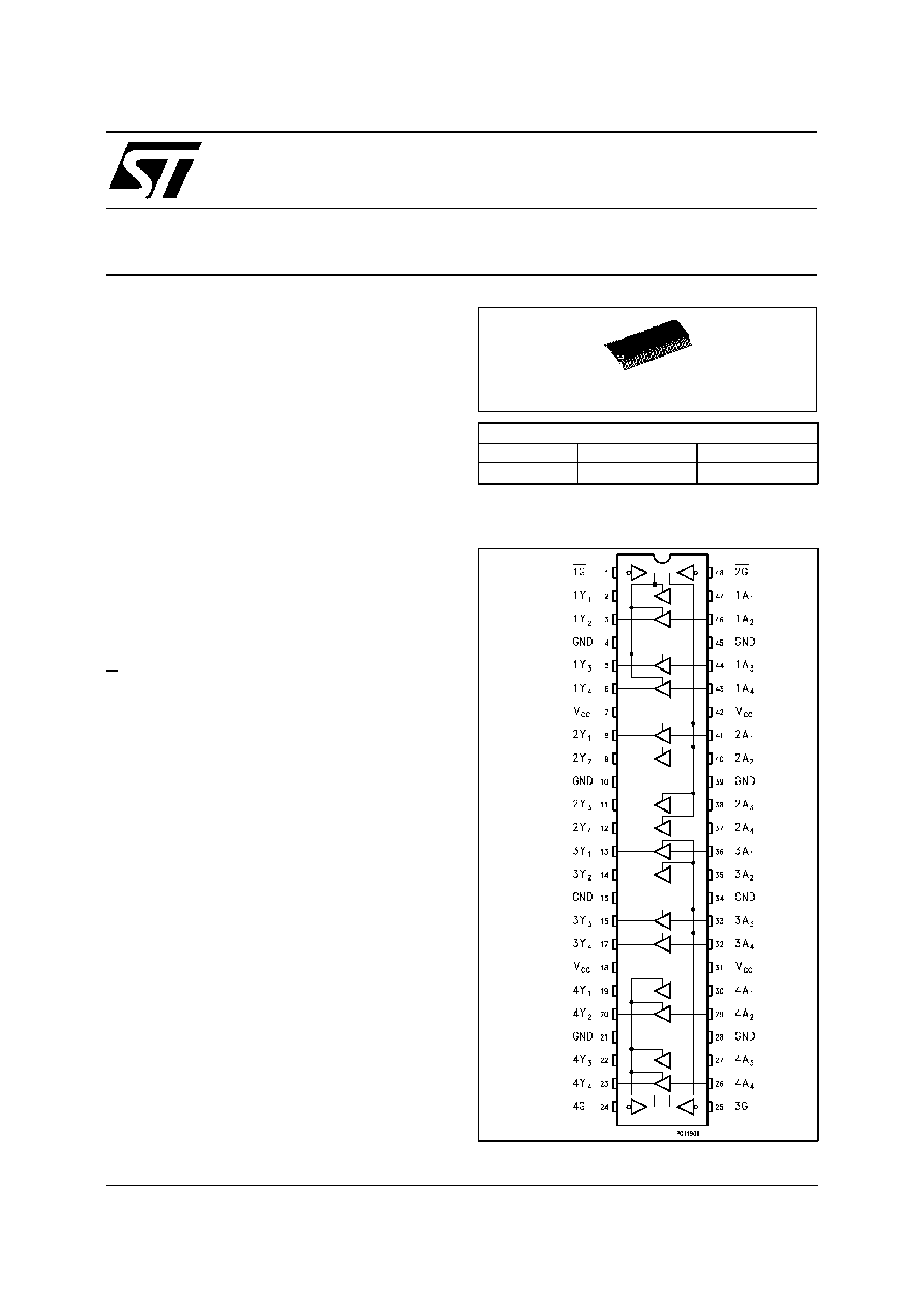
The ACT16244 is an advanced CMOS 16-BIT
BUS
BUFFER
(3-STATE)
fabricated
with
sub-micron silicon gate and double-layer metal
wiring C
2
MOS technology.
G output control governs four BUS BUFFERs.
The device is designed to be used with 3-state
memory address drivers, clock drivers, and
bus-oriented receivers and transmitters. The
device can be used as four 4-bit buffers, two 8-bit
buffers, or one 16-bit buffer.
The device is designed to interface directly High
Speed CMOS systems with TTL, NMOS and
CMOS output voltage levels.
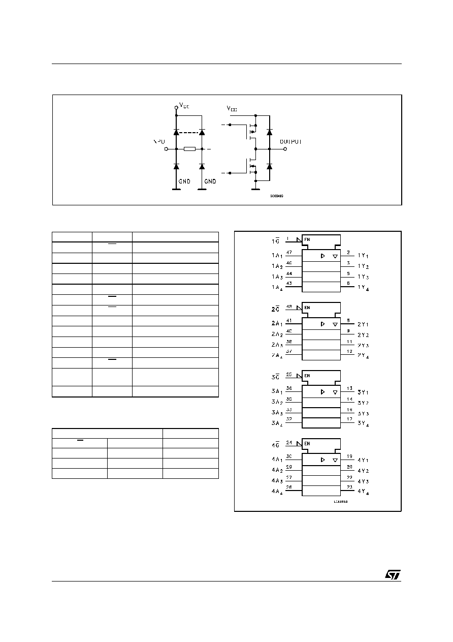
All inputs
and
outputs are
equipped with
protection circuits against static discharge, giving
them 2KV ESD immunity and transient excess
voltage.
TSSOP
PIN CONNECTION
ORDER CODES
PACKAGE
T UBE
T & R
TSSOP
74ACT16244TTR
1/8
ABSOLUTE MAXIMUM RATINGS
Symbol
Parameter
Val ue
Unit
V
CC
Supply Voltage
-0.5 to +7
V
V
I
DC Input Voltage
-0.5 to V
CC
+ 0.5
V
V
O
DC Output Voltage
-0.5 to V
CC
+ 0.5
V
I
IK
DC Input Diode Current
±
20
mA
I
OK
DC Output Diode Current
±
20
mA
I
O
DC Output Current
±
50
mA
I
CC
orI
GND
DC V
CC
or Ground Current
±
400
mA
T
stg
Storage Temperature
-65 to +150
o
C
T
L
Lead Temperature (10 sec)
300
o
C
Absolute Maximum Ratings are those values beyond which damage to the device may occur. Functional operation under these condition is not implied.
RECOMMENDED OPERATING CONDITIONS
Symbol
Parameter
Value
Unit
V
CC
Supply Voltage
4.5 to 5.5
V
V
I
Input Voltage
0 to V
CC
V
V
O
Output Voltage
0 to V
CC
V
T
op
Operating Temperature:
-40 to +85
o
C
dt/dv
Input Rise and Fall Time V
CC
= 4.5 to 5.5V (note 1)
8
ns/V
1) V
IN
from 0.8 V to 2.0 V
74ACT16244
3/8
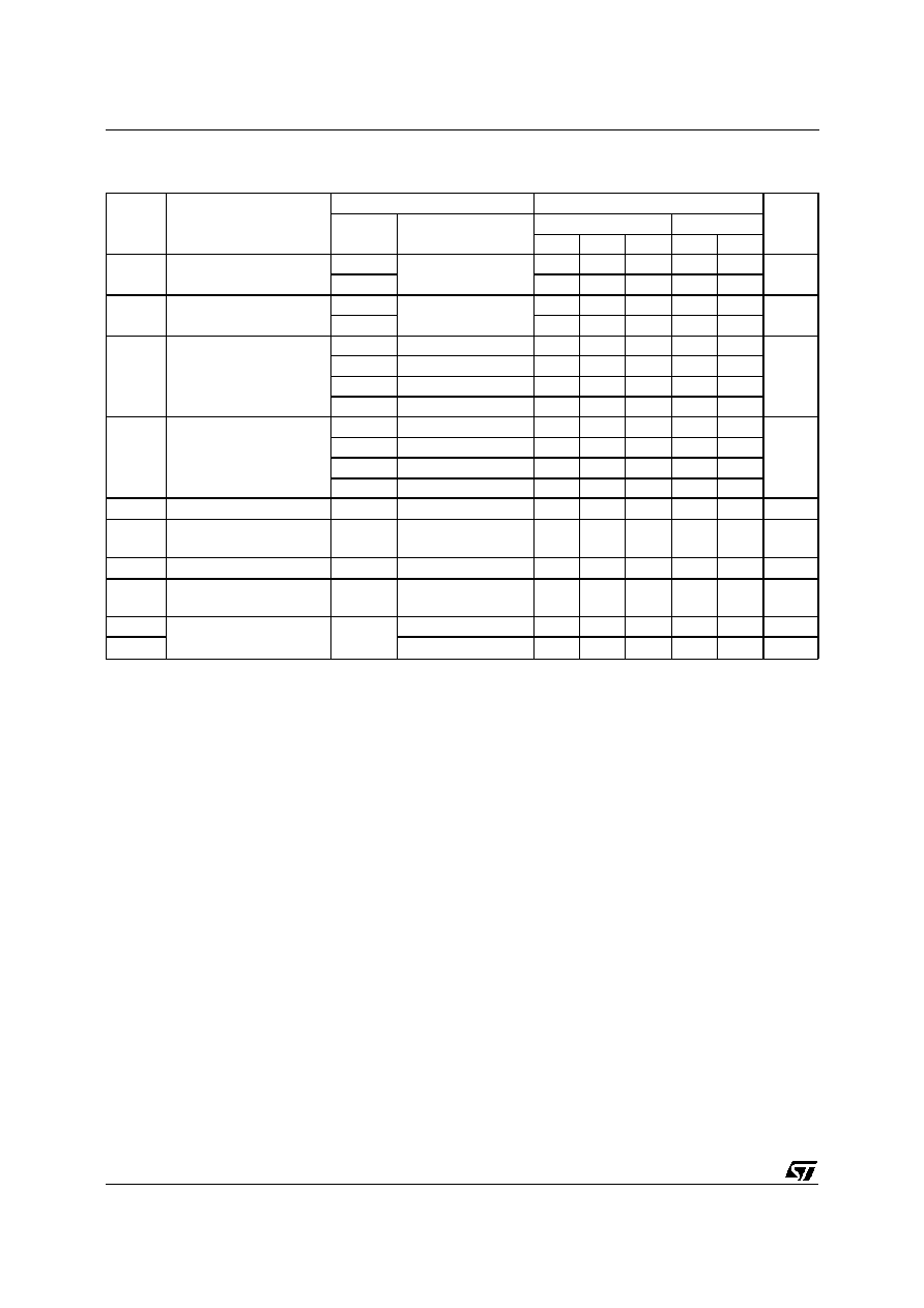
DC SPECIFICATIONS
Symb ol
Parameter
Test Co nditi ons
Valu e
Un it
V
CC
(V)
T
A
= 25
o
C
-40 to 85
o
C
Min.
T yp.
Max.
Mi n.
Max.
V
IH
High Level Input Voltage
4.5
V
O
= 0.1 V or
V
CC
- 0.1 V
2.0
2.0
V
5.5
2.0
2.0
V
IL
Low Level Input Voltage
4.5
V
O
= 0.1 V or
V
CC
- 0.1 V
0.8
0.8
V
5.5
0.8
0.8
V
OH
High Level Output
Voltage
4.5
I
O
=-50
µ
A
4.4
4.49
4.4
V
5.5
I
O
=-50
µ
A
5.4
5.49
5.4
4.5
I
O
=-24 mA
3.94
3.8
5.5
I
O
=-24 mA
4.94
4.8
V
OL
Low Level Output
Voltage
4.5
I
O
=50
µ
A
0.001
0.1
0.1
V
5.5
I
O
=50 mA
0.001
0.1
0.1
4.5
I
O
=24 mA
0.36
0.44
5.5
I
O
=24 mA
0.36
0.44
I
I
Input Leakage Current
5.5
V
I
= V
CC
orGND
±
0.1
±
1
µ
A
I
OZ
High Impedance Output
Leakage Current
5.5
V
I
= V
IH
orV
IL
V
O
= V
CC
orGND
±
0.5
±
5
µ
A
I
CCT
Max I
CC
/Input
5.5
V
I
= V
CC
-2.1V
0.9
1
mA
I
CC
Quiescent Supply
Current
5.5
V
I
= V
CC
orGND
8
80
µ
A
I
OLD
Dynamic Output Current
(note 1, 2)
5.5
V
OLD
= 1.65 V max
75
mA
I
OHD
V
OHD
= 3.85 V min
-75
mA
1) Maximum test duration 2ms, one output loaded attime
2) Incident wave switching is guaranteed on transmission lines with impedances as low as 50
.
74ACT16244
4/8
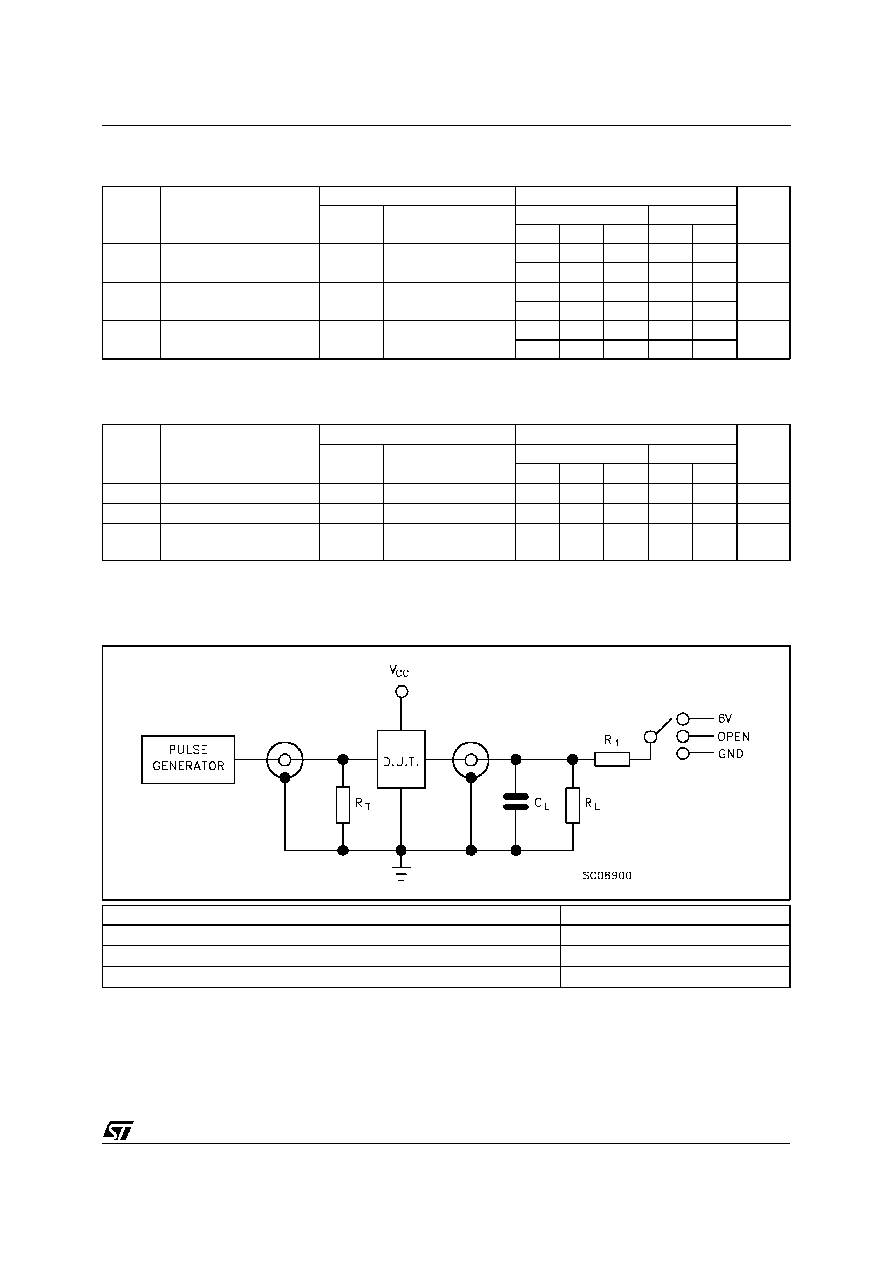
TEST CIRCUIT
T EST
SW IT CH
t
PLH
, t
PHL
Open
t
PZL
, t
PLZ
2V
CC
t
PZH
, t
PHZ
GND
C
L
= 50 pF or equivalent (includes jigand probe capacitance)
R
L
= R
1
= 500
orequivalent
R
T
= Z
OUT
of pulse generator (typically 50
)
CAPACITIVE CHARACTERISTICS
Symb ol
Parameter
Test Co nditi ons
Valu e
Un it
V
CC
(V)
T
A
= 25
o
C
-40 to 85
o
C
Min.
T yp.
Max.
Mi n.
Max.
C
IN
Input Capacitance
5.0
3.6
pF
C
OUT
Output Capacitance
5.0
11
pF
C
PD
Power Dissipation
Capacitance (note 1)
5.0
42
pF
1) C
PD
isdefined as the value of the IC'sinternal equivalent capacitance which is calculated fromthe operating current consumption without load. (Referto
Test Circuit).Average operating current can be obtained by the following equation. I
CC
(opr) = C
PD
∑
V
CC
∑
f
IN
+ I
CC
/16 (per circuit)
AC ELECTRICAL CHARACTERISTICS (C
L
= 50 pF, R
L
= 500
, Input t
r
= t
f
=3 ns)
Symb ol
Parameter
T est Con ditio n
Valu e
Un it
V
CC
(V)
T
A
= 25
o
C
-40 to 85
o
C
Min.
T yp.
Max.
Mi n.
Max.
t
PLH
t
PHL
Propagation Delay Time
5.0
(*)
2.0
3.3
5.0
2.0
6.0
ns
3.0
4.8
6.5
3.0
8.0
t
PZL
t
PZH
Output Enable Time
5.0
(*)
4.0
6.5
8.7
4.0
9.7
ns
3.0
5.5
7.7
3.0
8.8
t
PLZ
t
PHZ
Output Disable Time
5.0
(*)
4.0
6.0
8.0
4.0
9.2
ns
3.0
4.6
6.4
3.0
7.3
(*) Voltage range is 5V
±
0.5V
74ACT16244
5/8