1/9
July 2003
s
HIGH SPEED: t
PD
= 4.9ns (TYP.) at V
CC
= 5V
s
LOW POWER DISSIPATION:
I
CC
= 8
µ
A(MAX.) at T
A
=25∞C
s
COMPATIBLE WITH TTL OUTPUTS
V
IH
= 2V (MIN.), V
IL
= 0.8V (MAX.)
s
50
TRANSMISSION LINE DRIVING
CAPABILITY
s
SYMMETRICAL OUTPUT IMPEDANCE:
|I
OH
| = I
OL
= 24mA (MIN)
s
OPERATING VOLTAGE RANGE:
V
CC
(OPR) = 4.5V to 5.5V
s
IMPROVED LATCH-UP IMMUNITY
DESCRIPTION
The 74ACT16245 is an advanced high-speed
CMOS 16-BIT BUS TRANSCEIVER (3-STATE)
fabricated
with
sub-micron silicon gate and
double-layer metal wiring C
2
MOS technology.
This IC is intended for two-way asynchronous
communication between data buses and the
direction of data transmission is determined by
DIR input. The enable inputs G can be used to
disable the device so that the buses are effectively
isolated.
All floating bus terminals during the Z-state must
be held HIGH or LOW.
All inputs and outputs are equipped with protec-
tion circuits against static discharge, giving them
2KV ESD immunity and transient excess voltage.
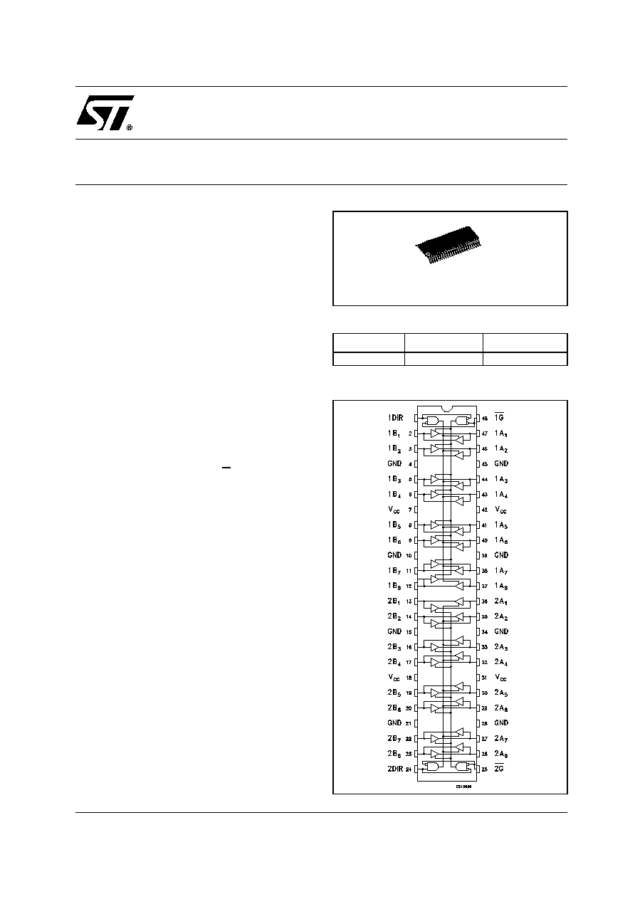
74ACT16245
16-BIT BUS TRANSCEIVER
WITH 3-STATE OUTPUTS (NON INVERTED)
ORDER CODES
PACKAGE
TUBE
T & R
TSSOP
74ACT16245TTR
TSSOP
PIN CONNECTION
74ACT16245
2/9
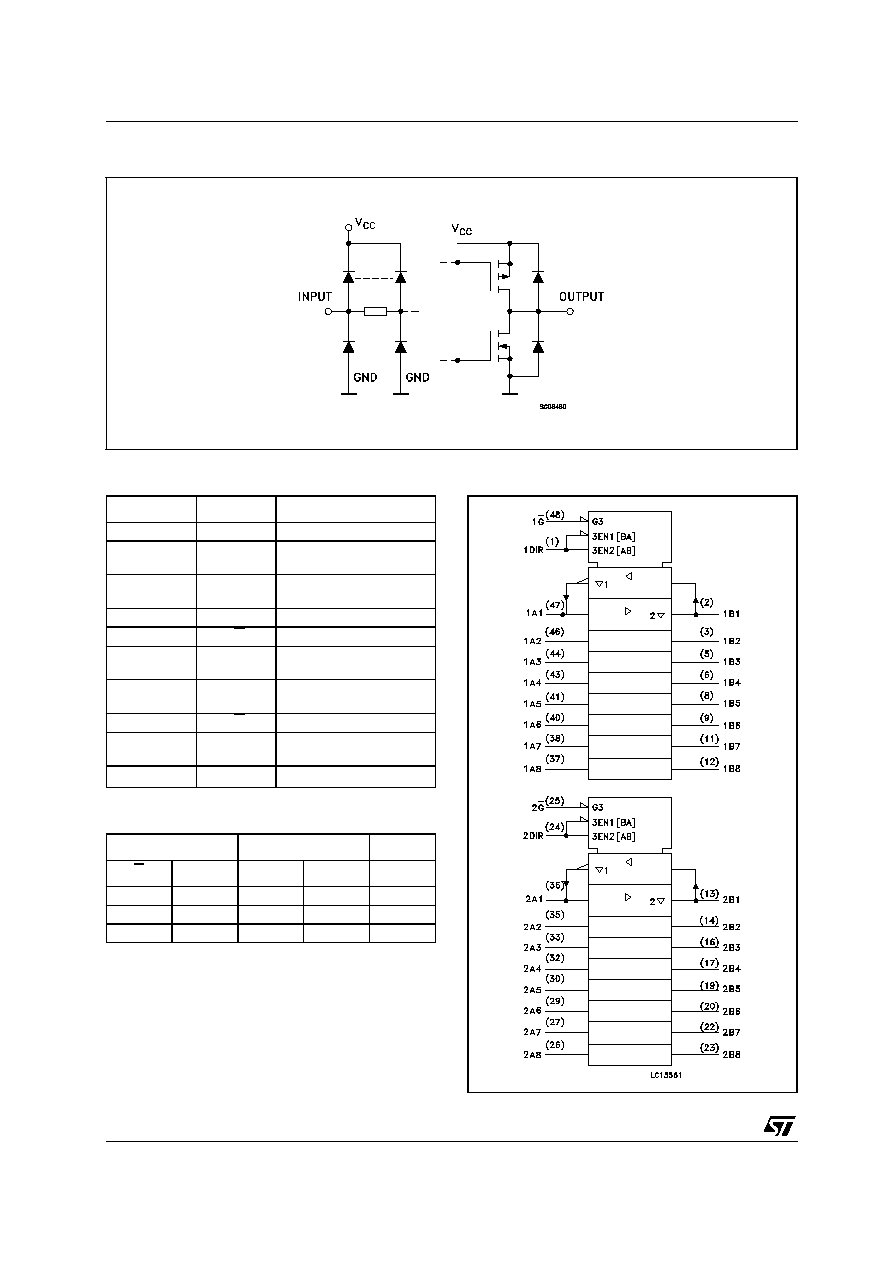
INPUT AND OUTPUT EQUIVALENT CIRCUIT
PIN DESCRIPTION
TRUTH TABLE
X : Don`t Care
Z : High Impedance
IEC LOGIC SYMBOLS
PIN No
SYMBOL
NAME AND FUNCTION
1
1DIR
Directional Control
2, 3, 5, 6, 8, 9,
11, 12
1B1 to 1B8 Data Inputs/Outputs
13, 14, 16, 17,
19, 20, 22, 23
2B1 to 2B8 Data Inputs/Outputs
24
2DIR
Directional Control
25
2G
Output Enable Input
36, 35, 33, 32,
30, 29, 27, 26
2A1 to 2A8 Data Inputs/Outputs
47, 46, 44, 43,
41, 40, 38, 38
1A1 to 1A8 Data Inputs/Outputs
48
1G
Output Enable Input
4, 10, 15, 21,
28, 34, 39, 45
GND
Ground (0V)
7, 18, 31, 42
V
CC
Positive Supply Voltage
INPUTS
FUNCTION
OUTPUT
G
DIR
A BUS
B BUS
Yn
L
L
OUTPUT
INPUT
A = B
L
H
INPUT
OUTPUT
B = A
H
X
Z
Z
Z
74ACT16245
3/9
ABSOLUTE MAXIMUM RATINGS
Absolute Maximum Ratings are those values beyond which damage to the device may occur. Functional operation under these conditions is
not implied.
RECOMMENDED OPERATING CONDITIONS
1) V
IN
from 0.8V to 2.0V
Symbol
Parameter
Value
Unit
V
CC
Supply Voltage
-0.5 to +7
V
V
I
DC Input Voltage
-0.5 to V
CC
+ 0.5
V
V
O
DC Output Voltage
-0.5 to V
CC
+ 0.5
V
I
IK
DC Input Diode Current
±
20
mA
I
OK
DC Output Diode Current
±
20
mA
I
O
DC Output Current
±
50
mA
I
CC
or I
GND
DC V
CC
or Ground Current
±
400
mA
T
stg
Storage Temperature
-65 to +150
∞C
T
L
Lead Temperature (10 sec)
300
∞C
Symbol
Parameter
Value
Unit
V
CC
Supply Voltage
4.5 to 5.5
V
V
I
Input Voltage
0 to V
CC
V
V
O
Output Voltage
0 to V
CC
V
T
op
Operating Temperature
-55 to 125
∞C
dt/dv
Input Rise and Fall Time V
CC
= 4.5 to 5.5V (note 1)
8
ns/V
74ACT16245
4/9
DC SPECIFICATIONS
1) Maximum test duration 2ms, one output loaded at time
2) Incident wave switching is guaranteed on transmission lines with impedances as low as 50
AC ELECTRICAL CHARACTERISTICS (C
L
= 50 pF, R
L
= 500
, Input t
r
= t
f
= 3ns)
(*) Voltage range is 5.0V
±
0.5V
Symbol
Parameter
Test Condition
Value
Unit
V
CC
(V)
T
A
= 25∞C
-40 to 85∞C
-55 to 125∞C
Min.
Typ.
Max.
Min.
Max.
Min.
Max.
V
IH
High Level Input
Voltage
4.5
V
O
= 0.1 V or
V
CC
-0.1V
2.0
1.5
2.0
2.0
V
5.5
2.0
1.5
2.0
2.0
V
IL
Low Level Input
Voltage
4.5
V
O
= 0.1 V or
V
CC
-0.1V
1.5
0.8
0.8
0.8
5.5
1.5
0.8
0.8
0.8
V
V
OH
High Level Output
Voltage
4.5
I
O
=-50
µ
A
4.4
4.49
4.4
4.4
5.5
I
O
=-50
µ
A
5.4
5.49
5.4
5.4
4.5
I
O
=-24 mA
3.86
3.76
3.7
V
5.5
I
O
=-24 mA
4.86
4.76
4.7
V
OL
Low Level Output
Voltage
4.5
I
O
=50
µ
A
0.001
0.1
0.1
0.1
5.5
I
O
=50
µ
A
0.001
0.1
0.1
0.1
4.5
I
O
=24 mA
0.36
0.44
0.5
5.5
I
O
=24 mA
0.36
0.44
0.5
I
I
Input Leakage Cur-
rent
5.5
V
I
= V
CC
or GND
±
0.1
±
1
±
1
µ
A
I
OZ
High Impedance
Output Leakage
Current
5.5
V
I
= V
IH
or V
IIL
V
O
= V
CC
or GND
±
0.5
±
5
±
10
µ
A
I
CCT
Max I
CC
/Input
5.5
V
I
= V
CC
- 2.1V
0.6
1.5
1.6
mA
I
CC
Quiescent Supply
Current
5.5
V
I
= V
CC
or GND
8
80
160
µ
A
I
OLD
Dynamic Output
Current (note 1, 2)
5.5
V
OLD
= 1.65 V max
75
50
mA
I
OHD
V
OHD
= 3.85 V min
-75
-50
mA
Symbol
Parameter
Test Condition
Value
Unit
V
CC
(V)
T
A
= 25∞C
-40 to 85∞C
-55 to 125∞C
Min.
Typ.
Max.
Min.
Max.
Min.
Max.
t
PLH
Propagation Delay
Time
5.0
(*)
3.5
4.6
10.5
11.5
ns
t
PHL
4.8
6.5
10.2
11.1
t
PZL
Output Enable
Time
5.0
(*)
6.1
9.2
11.6
12.6
ns
t
PZH
5.5
8.0
10.0
10.9
t
PLZ
Output Disable-
Time
5.0
(*)
5.6
8.3
11.8
12.7
ns
t
PHZ
5.0
7.3
12.6
13.4

74ACT16245
5/9
CAPACITIVE CHARACTERISTICS
1) C
PD
is defined as the value of the IC's internal equivalent capacitance which is calculated from the operating current consumption without
load. (Refer to Test Circuit). Average operating current can be obtained by the following equation. I
CC(opr)
= C
PD
x V
CC
x f
IN
+ I
CC
/16 (per
circuit)
TEST CIRCUIT
C
L
= 50pF or equivalent (includes jig and probe capacitance)
R
L
= R
1
= 500
or equivalent
R
T
= Z
OUT
of pulse generator (typically 50
)
Symbol
Parameter
Test Condition
Value
Unit
V
CC
(V)
T
A
= 25∞C
-40 to 85∞C
-55 to 125∞C
Min.
Typ.
Max.
Min.
Max.
Min.
Max.
C
IN
Input Capacitance
5.0
6
pF
C
I/O
I/O Capacitance
5.0
14
pF
C
PD
Power Dissipation
Capacitance (note
1)
5.0
f
IN
= 10MHz
24
pF
Test
Switch
t
PLH,
t
PHL
Open
t
PZL,
t
PLZ
2V
CC
t
PZH,
t
PHZ
GND