1/10
July 2001
s
HIGH SPEED:
t
PD
= 5.8 ns (TYP.) at V
CC
= 3.3 V
s
COMPATIBLE WITH TTL OUTPUTS
s
LOW POWER DISSIPATION:
I
CC
= 4
µ
A (MAX.) at T
A
=25∞C
s
LOW NOISE:
V
OLP
= 0.5V (TYP.) at V
CC
= 3.3V
s
75
TRANSMISSION LINE DRIVING
CAPABILITY
s
SYMMETRICAL OUTPUT IMPEDANCE:
|I
OH
| = I
OL
= 12mA (MIN) at V
CC
= 3.0 V
s
PCI BUS LEVELS GUARANTEED AT 24 mA
s
BALANCED PROPAGATION DELAYS:
t
PLH
t
PHL
s
OPERATING VOLTAGE RANGE:
V
CC
(OPR) = 2V to 3.6V (1.2V Data Retention)
s
PIN AND FUNCTION COMPATIBLE WITH
74 SERIES 573
s
IMPROVED LATCH-UP IMMUNITY
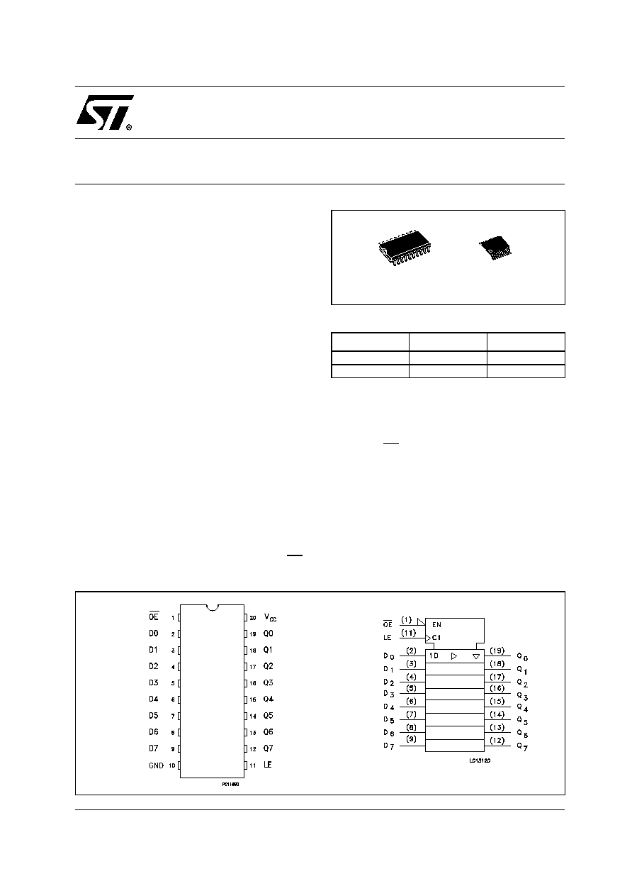
DESCRIPTION
The 74LVQ573 is a low voltage CMOS OCTAL
D-TYPE LATCH with 3 STATE OUTPUTS NON
INVERTING fabricated with sub-micron silicon
gate and double-layer metal wiring C
2
MOS
technology. It is ideal for low power and low noise
3.3V applications.
These 8 bit D-Type latch are controlled by a latch
enable input (LE) and an output enable input (OE).
While the LE input is held at a high level, the Q
outputs will follow the data input precisely.
When the LE is taken low, the Q outputs will be
latched precisely at the logic level of D input data.
While the (OE) input is low, the 8 outputs will be in
a normal logic state (high or low logic level) and
while high level the outputs will be in a high
impedance state. In order to enhance PC board
layout, the 74LVQ573 offers a pinout having inputs
and outputs on opposite side of the package.
All inputs and outputs are equipped with
protection circuits against static discharge, giving
them 2KV ESD immunity and transient excess
voltage.
74LVQ573
LOW VOLTAGE CMOS OCTAL D-TYPE LATCH
WITH 3 STATE OUTPUTS NON INVERTING
PIN CONNECTION AND IEC LOGIC SYMBOLS
ORDER CODES
PACKAGE
TUBE
T & R
SOP
74LVQ573M
74LVQ573MTR
TSSOP
74LVQ573TTR
TSSOP
SOP
74LVQ573
2/10
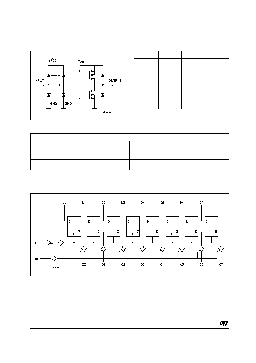
INPUT AND OUTPUT EQUIVALENT CIRCUIT
PIN DESCRIPTION
TRUTH TABLE
X : Don't Care
Z : High Impedance
* : Q outputs are latched at the time when the LE input is taken low logic level
LOGIC DIAGRAM
PIN No
SYMBOL
NAME AND FUNCTION
1
OE
3 State Output Enable
Input (Active LOW)
2, 3, 4, 5, 6,
7, 8, 9
D0 to D7
Data Inputs
12, 13, 14,
15, 16, 17,
18, 19
Q0 to Q7
3-State Latch Outputs
11
LE
Latch Enable Input
10
GND
Ground (0V)
20
V
CC
Positive Supply Voltage
INPUTS
OUTPUT
OE
LE
D
Q
H
X
X
Z
L
L
X
NO CHANGE*
L
H
L
L
L
H
H
H

74LVQ573
3/10
ABSOLUTE MAXIMUM RATINGS
Absolute Maximum Ratings are those values beyond which damage to the device may occur. Functional operation under these conditions is
not implied
RECOMMENDED OPERATING CONDITIONS
1) Truth Table guaranteed: 1.2V to 3.6V
2) V
IN
from 0.8V to 2V
DC SPECIFICATIONS
1) Maximum test duration 2ms, one output loaded at time
2) Incident wave switching is guaranteed on transmission lines with impedances as low as 75
Symbol
Parameter
Value
Unit
V
CC
Supply Voltage
-0.5 to +7
V
V
I
DC Input Voltage
-0.5 to V
CC
+ 0.5
V
V
O
DC Output Voltage
-0.5 to V
CC
+ 0.5
V
I
IK
DC Input Diode Current
±
20
mA
I
OK
DC Output Diode Current
±
20
mA
I
O
DC Output Current
±
50
mA
I
CC
or I
GND
DC V
CC
or Ground Current
±
400
mA
T
stg
Storage Temperature
-65 to +150
∞C
T
L
Lead Temperature (10 sec)
300
∞C
Symbol
Parameter
Value
Unit
V
CC
Supply Voltage (note 1)
2 to 3.6
V
V
I
Input Voltage
0 to V
CC
V
V
O
Output Voltage
0 to V
CC
V
T
op
Operating Temperature
-55 to 125
∞C
dt/dv
Input Rise and Fall Time V
CC
= 3.0V (note 2)
0 to 10
ns/V
Symbol
Parameter
Test Condition
Value
Unit
V
CC
(V)
T
A
= 25∞C
-40 to 85∞C
-55 to 125∞C
Min.
Typ.
Max.
Min.
Max.
Min.
Max.
V
IH
High Level Input
Voltage
3.0 to
3.6
2.0
2.0
2.0
V
V
IL
Low Level Input
Voltage
0.8
0.8
0.8
V
V
OH
High Level Output
Voltage
3.0
I
O
=-50
µ
A
2.9
2.99
2.9
2.9
V
I
O
=-12 mA
2.58
2.48
2.48
I
O
=-24 mA
2.2
2.2
V
OL
Low Level Output
Voltage
3.0
I
O
=50
µ
A
0.002
0.1
0.1
0.1
V
I
O
=12 mA
0
0.36
0.44
0.44
I
O
=24 mA
0.55
0.55
I
I
Input Leakage
Current
3.6
V
I
= V
CC
or GND
±
0.1
±
1
±
1
µ
A
Ioz
High Impedance
Output Leakage
Current
3.6
V
I
= V
IH
or V
IL
V
O
= V
CC
or GND
±
0.25
±
2.5
±
5.0
µ
A
I
CC
Quiescent Supply
Current
3.6
V
I
= V
CC
or GND
4
40
40
µ
A
I
OLD
Dynamic Output
Current (note 1, 2)
3.6
V
OLD
= 0.8 V max
36
25
mA
I
OHD
V
OHD
= 2 V min
-25
-25
mA
74LVQ573
4/10
DYNAMIC SWITCHING CHARACTERISTICS
1) Worst case package.
2) Max number of outputs defined as (n). Data inputs are driven 0V to 3.3V, (n-1) outputs switching and one output at GND.
3) Max number of data inputs (n) switching. (n-1) switching 0V to 3.3V. Inputs under test switching: 3.3V to threshold (V
ILD
), 0V to threshold
(V
IHD
), f=1MHz.
AC ELECTRICAL CHARACTERISTICS (C
L
= 50 pF, R
L
= 500
, Input t
r
= t
f
= 3ns)
1) Skew is defined as the absolute value of the difference between the actual propagation delay for any two outputs of the same device switch-
ing in the same direction, either HIGH or LOW (t
OSLH
= |t
PLHm
- t
PLHn
|, t
OSHL
= |t
PHLm
- t
PHLn
|)
2) Parameter guaranteed by design
(*) Voltage range is 3.3V
±
0.3V
Symbol
Parameter
Test Condition
Value
Unit
V
CC
(V)
T
A
= 25∞C
-40 to 85∞C
-55 to 125∞C
Min.
Typ.
Max.
Min.
Max.
Min.
Max.
V
OLP
Dynamic Low
Voltage Quiet
Output (note 1, 2)
3.3
C
L
= 50 pF
0.5
0.8
V
V
OLV
-0.8
-0.6
V
IHD
Dynamic High
Voltage Input
(note 1, 3)
3.3
2
V
V
ILD
Dynamic Low
Voltage Input
(note 1, 3)
3.3
0.8
V
Symbol
Parameter
Test Condition
Value
Unit
V
CC
(V)
T
A
= 25∞C
-40 to 85∞C
-55 to 125∞C
Min.
Typ.
Max.
Min.
Max.
Min.
Max.
t
PLH
t
PHL
Propagation Delay
Time LE to Q
2.7
7.2
11.5
13.5
15.5
ns
3.3
(*)
5.8
9.0
10.5
12.0
t
PLH
t
PHL
Propagation Delay
Time D to Q
2.7
7.2
11.5
13.5
15.5
ns
3.3
(*)
5.8
9.0
10.5
12.0
t
PLZ
t
PHZ
Output Disable
Time
2.7
8.7
14.0
16.0
18.5
ns
3.3
(*)
7.4
11.5
13.5
15.5
t
PZL
t
PZH
Output Enable
Time
2.7
8.5
14.0
16.0
18.5
ns
3.3
(*)
7.5
11.5
13.5
15.5
t
W
LE Pulse Width
HIGH
2.7
2.0
5.0
6.0
6.0
ns
3.3
(*)
1.5
4.0
4.0
4.0
t
sL
t
sH
Setup Time D to LE
HIGH or LOW
2.7
0.0
4.0
4.5
4.5
ns
3.3
(*)
0.0
3.0
3.0
3.0
t
hL
t
hH
Hold Time D to LE,
HIGH or LOW
2.7
0.0
1.5
1.5
1.5
ns
3.3
(*)
0.0
1.5
1.5
1.5
t
OSLH
t
OSHL
Output To Output
Skew Time
(note1, 2)
2.7
0.5
1.0
1.0
1.0
ns
3.3
(*)
0.5
1.0
1.0
1.0
74LVQ573
5/10
CAPACITIVE CHARACTERISTICS
1) C
PD
is defined as the value of the IC's internal equivalent capacitance which is calculated from the operating current consumption without
load. (Refer to Test Circuit). Average operating current can be obtained by the following equation. I
CC(opr)
= C
PD
x V
CC
x f
IN
+ I
CC
/n (per latch)
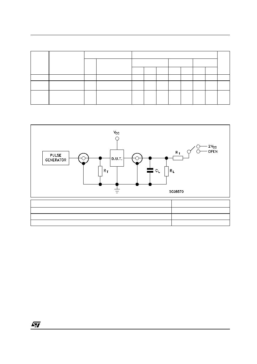
TEST CIRCUIT
C
L
= 50pF or equivalent (includes jig and probe capacitance)
R
L
= R
1
= 500
or equivalent
R
T
= Z
OUT
of pulse generator (typically 50
)
Symbol
Parameter
Test Condition
Value
Unit
V
CC
(V)
T
A
= 25∞C
-40 to 85∞C
-55 to 125∞C
Min.
Typ.
Max.
Min.
Max.
Min.
Max.
C
IN
Input Capacitance
3.3
4
pF
C
OUT
Output
Capacitance
3.3
8
pF
C
PD
Power Dissipation
Capacitance
(note 1)
3.3
f
IN
= 10MHz
10
pF
TEST
SWITCH
t
PLH
, t
PHL
Open
t
PZL
, t
PLZ
2V
CC
t
PZH
, t
PHZ
Open