1/8
June 2001
s
HIGH SPEED: t
PD
= 3.9 ns (TYP.) at V
CC
= 5V
s
LOW POWER DISSIPATION:
I
CC
= 2
µ
A (MAX.) at T
A
=25∞C
s
TYPICAL HYSTERESIS :
V
h
= 1V at V
CC
= 4.5V
s
POWER DOWN PROTECTION ON INPUTS
s
SYMMETRICAL OUTPUT IMPEDANCE:
|I
OH
| = I
OL
= 8 mA (MIN)
s
BALANCED PROPAGATION DELAYS:
t
PLH
t
PHL
s
OPERATING VOLTAGE RANGE:
V
CC
(OPR) = 2V to 5.5V
s
PIN AND FUNCTION COMPATIBLE WITH
74 SERIES 132
s
IMPROVED LATCH-UP IMMUNITY
s
LOW NOISE: V
OLP
= 0.8V (MAX.)
DESCRIPTION
The 74VHC132 is an advanced high-speed
CMOS QUAD 2-INPUT SCHMITT NAND GATE
fabricated with sub-micron silicon gate and
double-layer metal wiring C
2
MOS technology.
Power down protection is provided on all inputs
and 0 to 7V can be accepted on inputs with no
regard to the supply voltage. This device can be
used to interface 5V to 3V.
Pin configuration and function are the same as
those of the 74VHC00 but the 74VHC132 has
hysteresis.
This together with its schmitt trigger function
allows it to be used on line receivers with slow
rise/fall input signals.
All inputs and outputs are equipped with
protection circuits against static discharge, giving
them 2KV ESD immunity and transient excess
voltage.
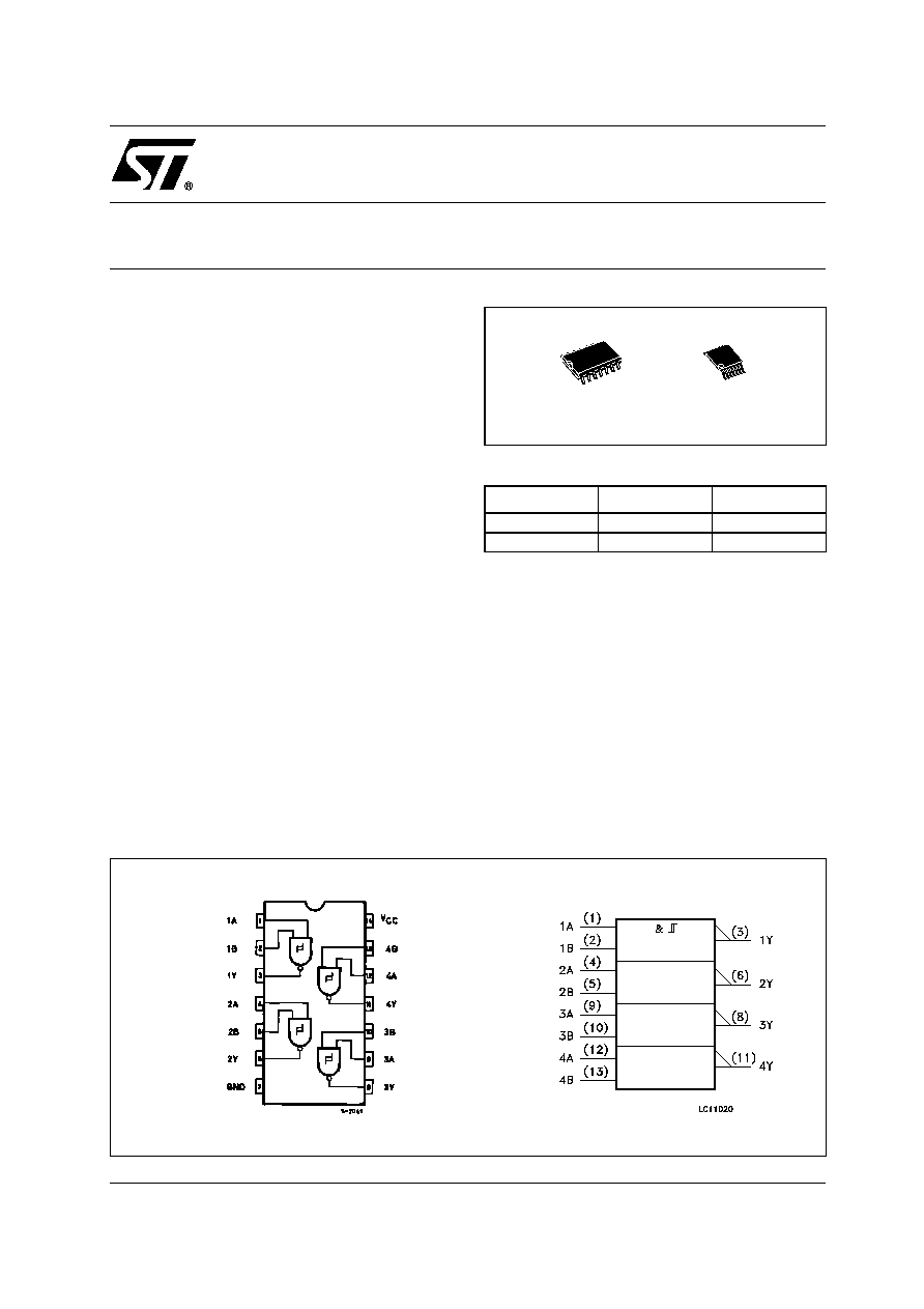
74VHC132
QUAD 2-INPUT SCHMITT NAND GATE
PIN CONNECTION AND IEC LOGIC SYMBOLS
ORDER CODES
PACKAGE
TUBE
T & R
SOP
74VHC132M
74VHC132MTR
TSSOP
74VHC132TTR
TSSOP
SOP
74VHC132
2/8
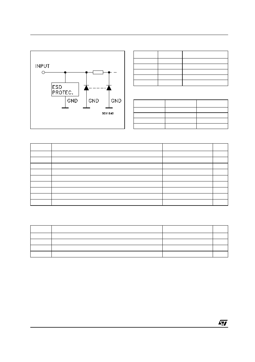
INPUT EQUIVALENT CIRCUIT
PIN DESCRIPTION
TRUTH TABLE
ABSOLUTE MAXIMUM RATINGS
Absolute Maximum Ratings are those values beyond which damage to the device may occur. Functional operation under these conditions is
not implied
RECOMMENDED OPERATING CONDITIONS
PIN No
SYMBOL
NAME AND FUNCTION
1, 4, 9, 12
1A to 4A
Data Inputs
2, 5, 10, 13
1B to 4B
Data Inputs
3, 6, 8, 11
1Y to 4Y
Data Outputs
7
GND
Ground (0V)
14
V
CC
Positive Supply Voltage
A
B
Y
L
L
H
L
H
H
H
L
H
H
H
L
Symbol
Parameter
Value
Unit
V
CC
Supply Voltage
-0.5 to +7.0
V
V
I
DC Input Voltage
-0.5 to +7.0
V
V
O
DC Output Voltage
-0.5 to V
CC
+ 0.5
V
I
IK
DC Input Diode Current
- 20
mA
I
OK
DC Output Diode Current
±
20
mA
I
O
DC Output Current
±
25
mA
I
CC
or I
GND
DC V
CC
or Ground Current
±
50
mA
T
stg
Storage Temperature
-65 to +150
∞C
T
L
Lead Temperature (10 sec)
300
∞C
Symbol
Parameter
Value
Unit
V
CC
Supply Voltage
2 to 5.5
V
V
I
Input Voltage
0 to 5.5
V
V
O
Output Voltage
0 to V
CC
V
T
op
Operating Temperature
-55 to 125
∞C
74VHC132
3/8
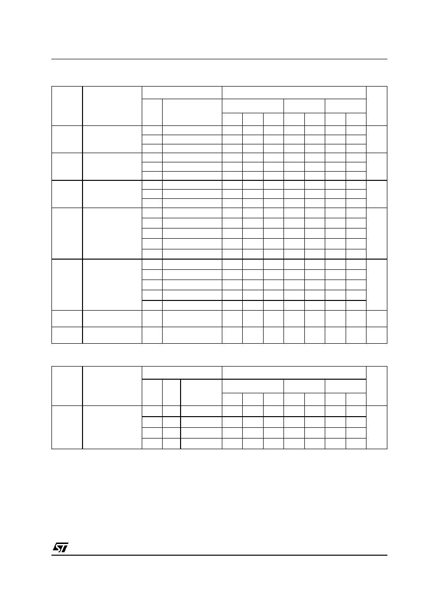
DC SPECIFICATIONS
AC ELECTRICAL CHARACTERISTICS (Input t
r
= t
f
= 3ns)
(*) Voltage range is 3.3V
±
0.3V
(**) Voltage range is 5.0V
±
0.5V
Symbol
Parameter
Test Condition
Value
Unit
V
CC
(V)
T
A
= 25∞C
-40 to 85∞C
-55 to 125∞C
Min.
Typ.
Max.
Min.
Max.
Min.
Max.
V
t+
High Level
Threshold Voltage
3.0
2.2
2.2
2.2
V
4.5
3.15
3.15
3.15
5.5
3.85
3.85
3.85
V
t-
Low Level
Threshold Voltage
3.0
0.9
0.9
0.9
V
4.5
1.35
1.35
1.35
5.5
1.65
1.65
1.65
V
h
Hysteresis Voltage
3.0
0.3
1.2
0.3
1.2
0.3
1.2
V
4.5
0.4
1.4
0.4
1.4
0.4
1.4
5.5
0.5
1.6
0.5
1.6
0.5
1.6
V
OH
High Level Output
Voltage
2.0
I
O
=-50
µ
A
1.9
2.0
1.9
1.9
V
3.0
I
O
=-50
µ
A
2.9
3.0
2.9
2.9
4.5
I
O
=-50
µ
A
4.4
4.5
4.4
4.4
3.0
I
O
=-4 mA
2.58
2.48
2.4
4.5
I
O
=-8 mA
3.94
3.8
3.7
V
OL
Low Level Output
Voltage
2.0
I
O
=50
µ
A
0.0
0.1
0.1
0.1
V
3.0
I
O
=50
µ
A
0.0
0.1
0.1
0.1
4.5
I
O
=50
µ
A
0.0
0.1
0.1
0.1
3.0
I
O
=4 mA
0.36
0.44
0.55
4.5
I
O
=8 mA
0.36
0.44
0.55
I
I
Input Leakage
Current
0 to
5.5
V
I
= 5.5V or GND
±
0.1
±
1
±
1
µ
A
I
CC
Quiescent Supply
Current
5.5
V
I
= V
CC
or GND
2
20
20
µ
A
Symbol
Parameter
Test Condition
Value
Unit
V
CC
(V)
C
L
(pF)
T
A
= 25∞C
-40 to 85∞C
-55 to 125∞C
Min.
Typ.
Max.
Min.
Max.
Min.
Max.
t
PLH
t
PHL
Propagation Delay
Time
3.3
(*)
15
5.6
11.9
1.0
14.0
1.0
14.0
ns
3.3
(*)
50
7.6
15.4
1.0
17.5
1.0
17.5
5.0
(**)
15
3.9
7.7
1.0
9.0
1.0
9.0
5.0
(**)
50
5.3
9.7
1.0
11.0
1.0
11.0
74VHC132
4/8
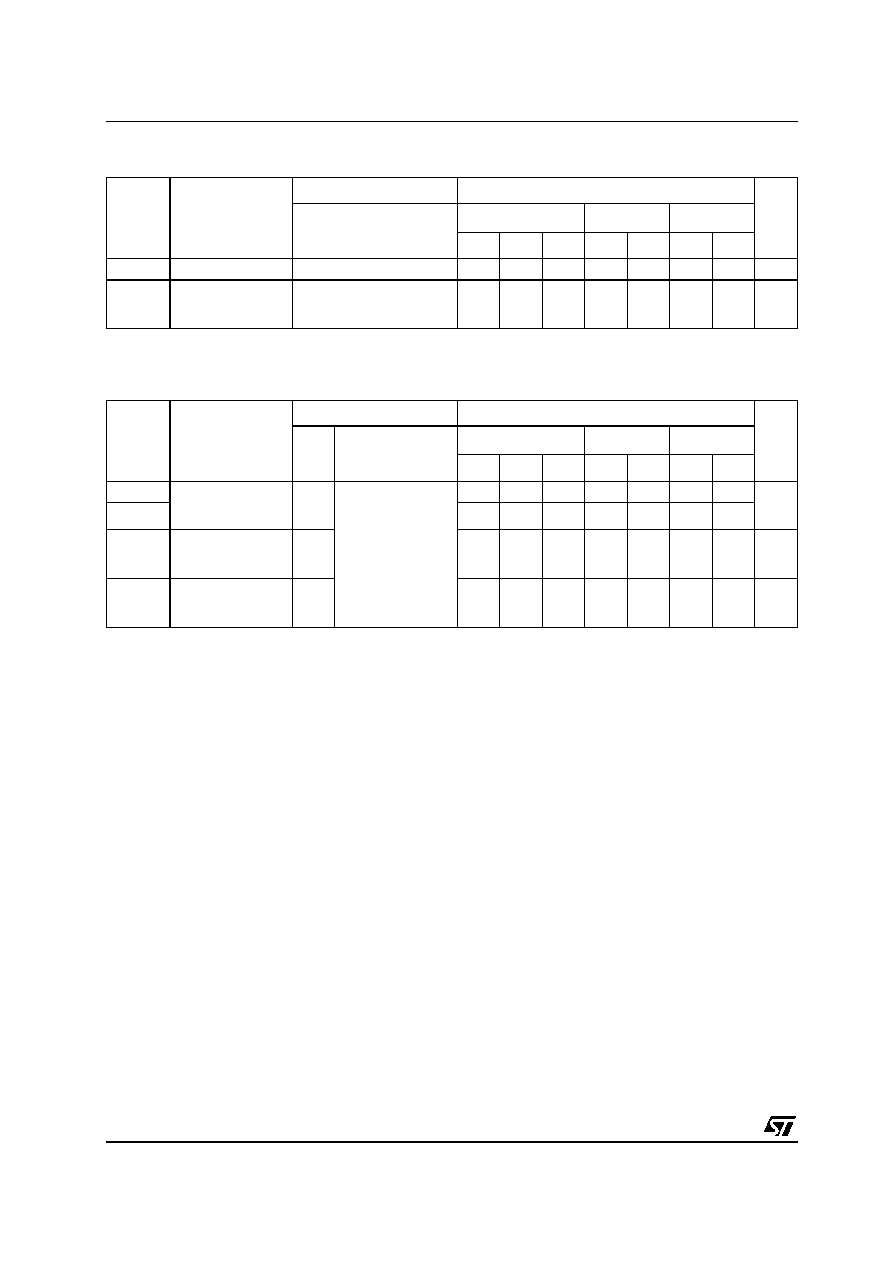
CAPACITIVE CHARACTERISTICS
1) C
PD
is defined as the value of the IC's internal equivalent capacitance which is calculated from the operating current consumption without
load. (Refer to Test Circuit). Average operating current can be obtained by the following equation. I
CC(opr)
= C
PD
x V
CC
x f
IN
+ I
CC
/4 (per gate)
DYNAMIC SWITCHING CHARACTERISTICS
1) Worst case package.
2) Max number of outputs defined as (n). Data inputs are driven 0V to 5.0V, (n-1) outputs switching and one output at GND.
3) Max number of data inputs (n) switching. (n-1) switching 0V to 5.0V. Inputs under test switching: 5.0V to threshold (V
ILD
), 0V to threshold
(V
IHD
), f=1MHz.
Symbol
Parameter
Test Condition
Value
Unit
T
A
= 25∞C
-40 to 85∞C
-55 to 125∞C
Min.
Typ.
Max.
Min.
Max.
Min.
Max.
C
IN
Input Capacitance
6
10
10
10
pF
C
PD
Power Dissipation
Capacitance
(note 1)
16
pF
Symbol
Parameter
Test Condition
Value
Unit
V
CC
(V)
T
A
= 25∞C
-40 to 85∞C
-55 to 125∞C
Min.
Typ.
Max.
Min.
Max.
Min.
Max.
V
OLP
Dynamic Low
Voltage Quiet
Output (note 1, 2)
5.0
C
L
= 50 pF
0.3
0.8
V
V
OLV
-0.8
-0.3
V
IHD
Dynamic High
Voltage Input
(note 1, 3)
5.0
3.5
V
V
ILD
Dynamic Low
Voltage Input
(note 1, 3)
5.0
1.5
V
74VHC132
5/8
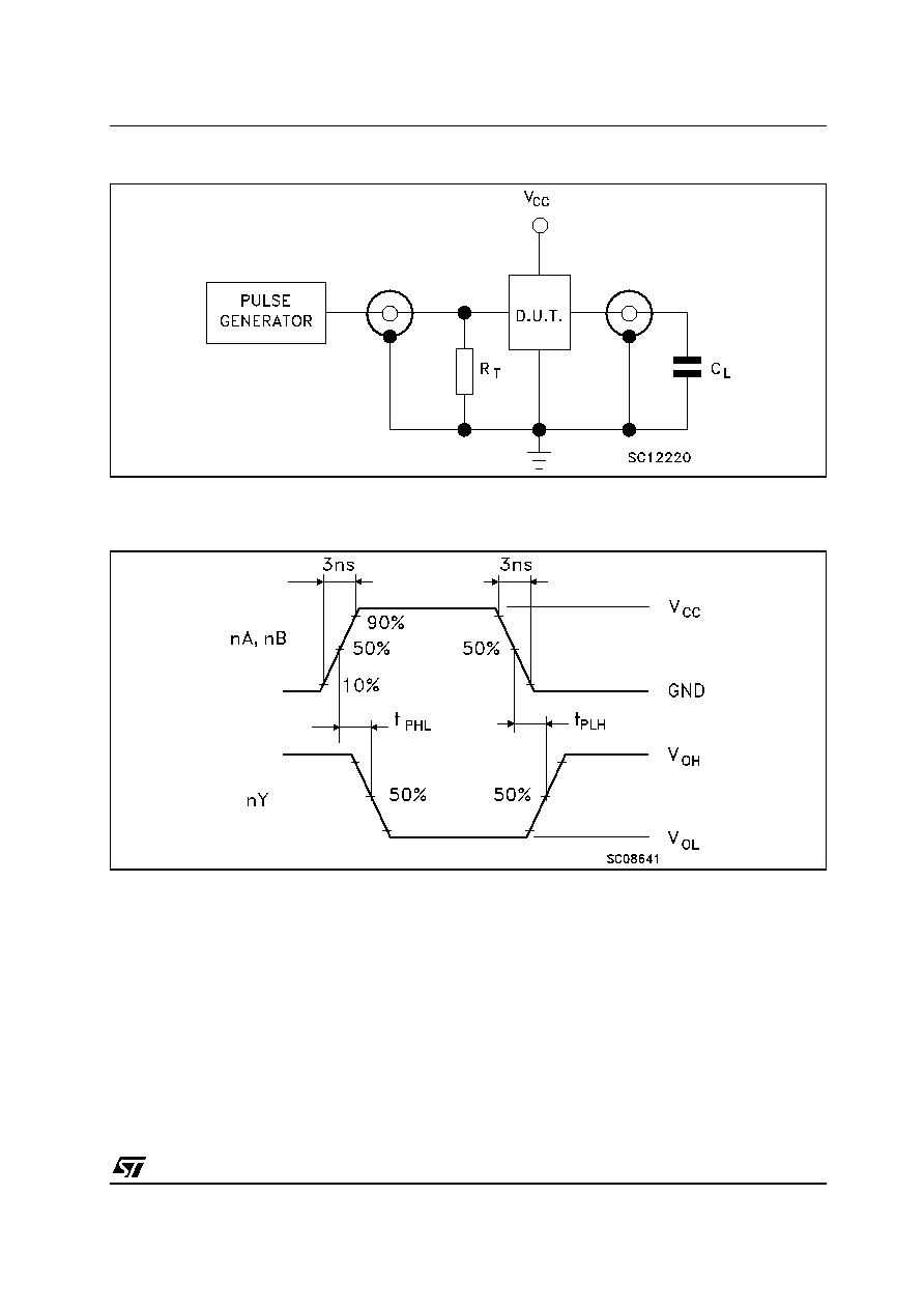
TEST CIRCUIT
C
L
=15/50pF or equivalent (includes jig and probe capacitance)
R
T
= Z
OUT
of pulse generator (typically 50
)
WAVEFORM: PROPAGATION DELAYS (f=1MHz; 50% duty cycle)