 | –≠–ª–µ–∫—Ç—Ä–æ–Ω–Ω—ã–π –∫–æ–º–ø–æ–Ω–µ–Ω—Ç: BAR43S | –°–∫–∞—á–∞—Ç—å:  PDF PDF  ZIP ZIP |

Æ
BAR 42
BAR 43, A, C, S
SMALL SIGNAL SCHOTTKY DIODES
DESCRIPTION
General purpose metal to silicon diodes featuring
very low turn-on voltage and fast switching.
June 1999 - Ed: 2A
Symbol
Parameter
Value
Unit
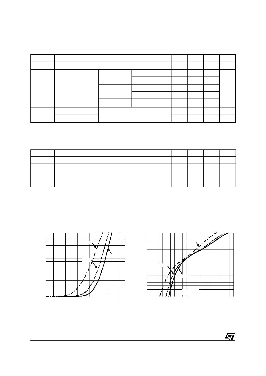
V
RRM
Repetitive peak reverse voltage
30
V
I
F
Continuous forward current
100
mA
I
FSM
Surge non repetitive forward current
tp=10ms sinusoidal
750
mA
P
tot
Power dissipation (note 1)
T
amb
= 25
∞
C
250
mW
T
stg
Maximum storage temperature range
- 65 to +150
∞
C
Tj
Maximum operating junction temperature *
150
∞
C
T
L
Maximum temperature for soldering during 10s
260
∞
C
Note 1: for double diodes, Ptot is the total power dissipation of both diodes.
ABSOLUTE RATINGS (limiting values)
SOT-23
(Plastic)
K
N.C.
A
K
A1
A1
A2
A
K1
K2
K2
K1
A2
BAR42/BAR43
BAR43A
BAR43C
BAR43S
* :
dPtot
dTj
<
1
Rth
(
j
-
a
)
thermal runaway condition for a diode on its own heatsink
Symbol
Test conditions
Value
Unit
R
th(j-a)
Junction-ambient *
500
∞
C/W
* Mounted on epoxy board with recommended pad layout.
THERMAL RESISTANCE
1/4
Symbol
Test Conditions
Min.
Typ.
Max.
Unit
V
BR
Tj = 25
∞
C
I
R
= 100
µ
A
30
V
V
F
*
Tj = 25
∞
C
BAR 42
I
F
= 10 mA
0.35
0.4
V
I
F
= 50 mA
0.5
0.65
BAR 43
I
F
= 2 mA
0.26
0.33
I
F
= 15 mA
0.45
All
I
F
= 100 mA
1
I
R
**
Tj = 25
∞
C
V
R
= 25V
500
nA
Tj = 100
∞
C
100
µ
A
Pulse test:
* tp = 380
µ
s,
< 2%
** tp = 5 ms,
<2%
STATIC CHARACTERISTICS
ELECTRICAL CHARACTERISTICS
Symbol
Test Conditions
Min.
Typ.
Max.
Unit
C
Tj = 25
∞
C
V
R
= 1V
F = 1MHz
7
pF
trr
Tj = 25
∞
C
I
F
= 10 mA
I
R
= 10 mA
I
rr
= 1mA
R
L
= 100
5
ns
*
Tj = 25
∞
C
R
L
= 50 K
C
L
= 300 pF
F = 45Mhz
V
i
= 2V
for BAR 43
80
%
* Detection efficiency.
DYNAMIC CHARACTERISTICS
0.00 0.05 0.10 0.15 0.20 0.25 0.30 0.35 0.40 0.45 0.50
0.00E+0
2.00E-3
4.00E-3
6.00E-3
8.00E-3
1.00E-2
1.20E-2
1.40E-2
1.60E-2
1.80E-2
2.00E-2
VFM(V)
IFM(A)
Tj=100
∞
C
Tj=50
∞
C
Tj=25
∞
C
Fig. 1-1: Forward voltage drop versus forward
current (typical values, low level).
0.0 0.1 0.2 0.3 0.4 0.5 0.6 0.7 0.8 0.9 1.0 1.1
1E-3
1E-2
1E-1
5E-1
VFM(V)
IFM(A)
Tj=100
∞
C
Tj=50
∞
C
Tj=25
∞
C
Fig. 1-2: Forward voltage drop versus forward
current (typical values, high level).
BAR 42/BAR 43, A, C, S
2/4
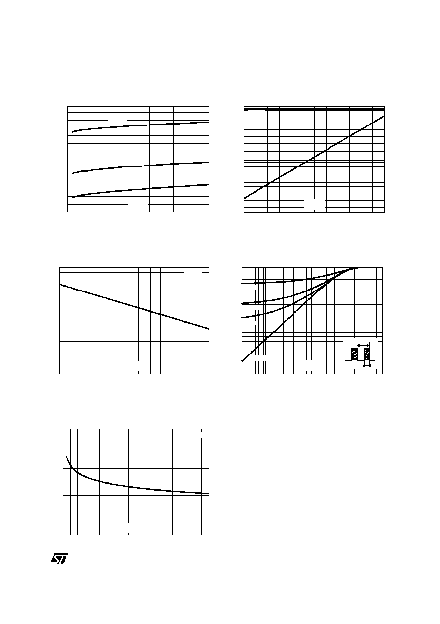
0
5
10
15
20
25
30
1E-2
1E-1
1E+0
1E+1
1E+2
VR(V)
IR(
µ
A)
Tj=50
∞
C
Tj=25
∞
C
Tj=100
∞
C
Fig. 2: Reverse leakage current versus reverse
voltage applied (typical values).
0
25
50
75
100
125
150
1E-2
1E-1
1E+0
1E+1
1E+2
1E+3
1E+4
Tj(
∞
C)
IR(
µ
A)
VR=30V
Fig. 3: Reverse leakage current versus junction
temperature.
1
2
5
10
20
30
1
2
5
10
VR(V)
C(pF)
F=1MHz
Tj=25
∞
C
Fi g . 4: Junction capacitance versus reverse
voltage applied (typical values).
1E-3
1E-2
1E-1
1E+0
1E+1
1E+2
0.01
0.10
1.00
tp(s)
Zth(j-a)/Rth(j-a)
T
=tp/T
tp
Single pulse
= 0.1
= 0.2
= 0.5
Fig. 5: Relative variation of thermal impedance
junction to ambient versus pulse duration (epoxy
FR4 with recommended pad layout, e(Cu)=35
µ
m).
0
5
10
15
20
25
30
35
40
45
50
150
200
250
300
350
S(Cu) (mm )
Rth(j-a) (
∞
C/W)
P=0.25W
Fig. 6: Thermal resistance junction to ambient
versus copper surface under each lead (Epoxy
printedcircuit board FR4, copper thickness:35
µ
m).
BAR 42/BAR 43, A, C, S
3/4
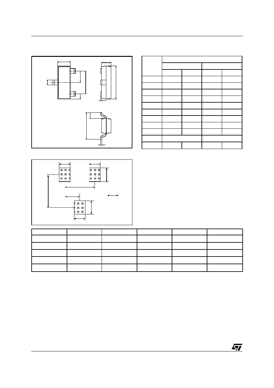
PACKAGE MECHANICAL DATA
SOT 23 (Plastic)
B
E
S
e
e1
A
D
c
L
H
A1
REF.
DIMENSIONS
Millimeters
Inches
Min.
Max.
Min.
Max.
A
0.89
1.4
0.035
0.055
A1
0
0.1
0
0.004
B
0.3
0.51
0.012
0.02
c
0.085
0.18
0.003
0.007
D
2.75
3.04
0.108
0.12
e
0.85
1.05
0.033
0.041
e1
1.7
2.1
0.067
0.083
E
1.2
1.6
0.047
0.063
H
2.1
2.75
0.083
0.108
L
0.6 typ.
0.024 typ.
S
0.35
0.65
0.014
0.026
Information furnished is believed to be accurate and reliable. However, STMicroelectronics assumes no responsibility for the consequences of
use of such information nor for any infringement of patents or other rights of third parties which may result from its use. No license is granted
by implication or otherwise under any patent or patent rights of STMicroelectronics. Specifications mentioned in this publication are subject to
change without notice. This publication supersedes and replaces all information previously supplied.
STMicroelectronics products are not authorized for use as critical components in lifesupport devices or systems without express writtenapproval
of STMicroelectronics.
The ST logo is a registered trademark of STMicroelectronics
©
1999 STMicroelectronics - Printed in Italy - All rights reserved.
STMicroelectronics GROUP OF COMPANIES
Australia - Brazil - China - Finland - France - Germany - Hong Kong - India - Italy - Japan - Malaysia
Malta - Morocco - Singapore - Spain - Sweden - Switzerland - United Kingdom - U.S.A.
http://www.st.com
FOOT PRINT DIMENSIONS
0.9
0.035
0.9
0.035
1.9
0.075
mm
inch
2.35
0.92
1.1
0.043
1.1
0.043
1.45
0.037
0.9
0.035
Ordering type
Marking
Package
Weight
Base qty
Delivery mode
BAR42
D94
SOT-23
0.01g
3000
Tape & reel
BAR43
D95
SOT-23
0.01g
3000
Tape & reel
BAR43S
DB1
SOT-23
0.01g
3000
Tape & reel
BAR43C
DB2
SOT-23
0.01g
3000
Tape & reel
BAR43S
DA5
SOT-23
0.01g
3000
Tape & reel
Epoxy meets UL94,V0
BAR 42/BAR 43, A, C, S
4/4