BUL1203E
HIGH VOLTAGE FAST-SWITCHING
NPN POWER TRANSISTOR
s
HIGH VOLTAGE CAPABILITY
s
LOW SPREAD OF DYNAMIC PARAMETERS
s
MINIMUM LOT-TO-LOT SPREAD FOR
RELIABLE OPERATION
s
VERY HIGH SWITCHING SPEED
APPLICATIONS
s
ELECTRONIC BALLASTS FOR
FLUORESCENT LIGHTING (277 V HALF
BRIDGE AND 120 V PUSH-PULL
TOPOLOGIES)
DESCRIPTION
The BUL1203E is a new device manufactured
using Diffused Collector technology to enhance
switching speeds and tight h
FE
range while
maintaining a wide RBSOA.
Thanks to his structure it has an intrinsic
ruggedness which enables the transistor to
withstand a high collector current level during
Breakdown condition, without using the transil
protection usually necessary in typical converters
for lamp ballast.
Æ
INTERNAL SCHEMATIC DIAGRAM
December 2003
ABSOLUTE MAXIMUM RATINGS
Symbol
Parameter
Value
Unit
V
CBO
Collector-BaseVoltage (I
E
= 0)
1200
V
V
CES
Collector-Emitter Voltage (V
BE
= 0)
1200
V
V
CEO
Collector-Emitter Voltage (I
B
= 0)
550
V
V
EBO
Emitter-Base Voltage (I
C
= 0)
9
V
I
C
Collector Current
5
A
I
CM
Collector Peak Current (t
p
< 5 ms)
8
A
I
B
Base Current
2
A
I
BM
Base Peak Current (t
p
< 5 ms)
4
A
P
tot
Total Dissipation at T
c
= 25
o
C
100
W
T
stg
Storage Temperature
-65 to 150
o
C
T
j
Max. Operating Junction Temperature
150
o
C
1
2
3
TO-220
1/7

THERMAL DATA
R
thj-case
Thermal Resistance Junction-case Max
1.25
o
C/W
ELECTRICAL CHARACTERISTICS (T
case
= 25
o
C unless otherwise specified)
Symbol
Parameter
Test Conditions
Min.
Typ.
Max.
Unit
I
CES
Collector Cut-off
Current (V
BE
= 0)
V
CE
= 1200 V
100
µ
A
I
CEO
Collector Cut-off
Current (I
B
= 0)
V
CE
= 550 V
100
µ
A
V
CEO(sus)
Collector-Emitter
Sustaining Voltage
(I
B
= 0)
I
C
= 100 mA L = 25 mH
550
V
V
EBO
Emitter-Base Voltage
(I
C
= 0)
I
E
= 10 mA
9
V
V
CE(sat)
Collector-Emitter
Saturation Voltage
I
C
= 1 A I
B
= 0.2 A
I
C
= 2 A I
B
= 0.4 A
I
C
= 3 A I
B
= 1 A
0.5
0.7
1.5
V
V
V
V
BE(sat)
Base-Emitter
Saturation Voltage
I
C
= 2 A I
B
= 0.4 A
I
C
= 3 A I
B
= 1 A
1.5
1.5
V
V
h
FE
DC Current Gain
I
C
= 1 mA V
CE
= 5 V
I
C
= 10 mA V
CE
= 5 V
I
C
= 0.8 A V
CE
= 3 V
I
C
= 2 A V
CE
= 5 V
10
10
14
9
32
28
t
on
t
s
t
f
RESISTIVE LOAD
Turn-on Time
Storage Time
Fall Time
I
C
= 2 A I
B1
= 0.4 A
I
B2
= -0.8 A tp = 30
µ
s
V
CC
= 150 V (see figure 2)
2.5
0.2
0.5
3.0
0.3
µ
s
µ
s
µ
s
E
ar
Repetitive Avalanche
Energy
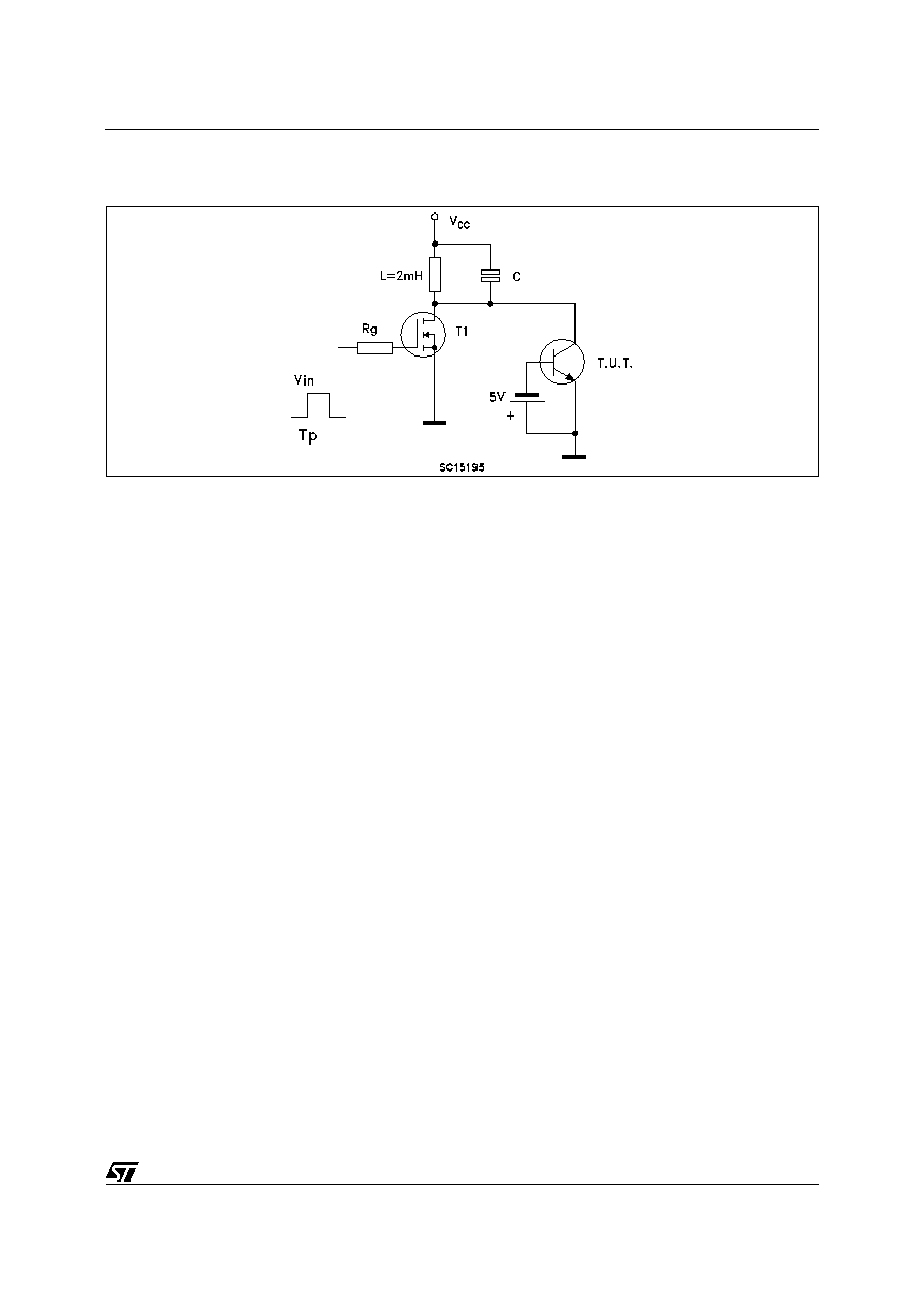
L = 2 mH C = 1.8 nF
V
CC
= 50 V V
BE
= -5 V
(see figure 3)
6
mJ
Pulsed: Pulse duration = 300
µ
s, duty cycle 1.5 %
Safe Operating Area
Derating Curve
BUL1203E
2/7

DC Current Gain
DC Current Gain
Collector-Emitter Saturation Voltage
Base-Emitter Saturation Voltage
Inductive Load Storage Time
Inductive Load Fall Time
BUL1203E
3/7

Figure 1: Inductive Load Switching Test Circuit
Reverse Biased Safe Operating Area
Figure 2: Resistive Load Switching Test Circuit
BUL1203E
4/7