BUL381D
BUL382D
HIGH VOLTAGE FAST-SWITCHING
NPN POWER TRANSISTORS
s
SGS-THOMSON PREFERRED SALESTYPES
s
HIGH VOLTAGE CAPABILITY
s
LOW SPREAD OF DYNAMIC PARAMETERS
s
MINIMUM LOT-TO-LOT SPREAD FOR
RELIABLE OPERATION
s
VERY HIGH SWITCHING SPEED
s
LARGE RBSOA
s
INTEGRATED ANTIPARALLEL
COLLECTOR-EMITTER DIODE
APPLICATIONS
s
ELECTRONIC TRANSFORMERS FOR
HALOGEN LAMPS
s
ELECTRONIC BALLASTS FOR
FLUORESCENT LIGHTING
s
SWITCH MODE POWER SUPPLIES
DESCRIPTION
The BUL381D and BUL382D are manufactured
using
high
voltage
Multi
Epitaxial
Planar
technology for high switching speeds and high
voltage capability.
The BUL series is designed for use in lighting
applications and low cost switch-mode power
supplies.
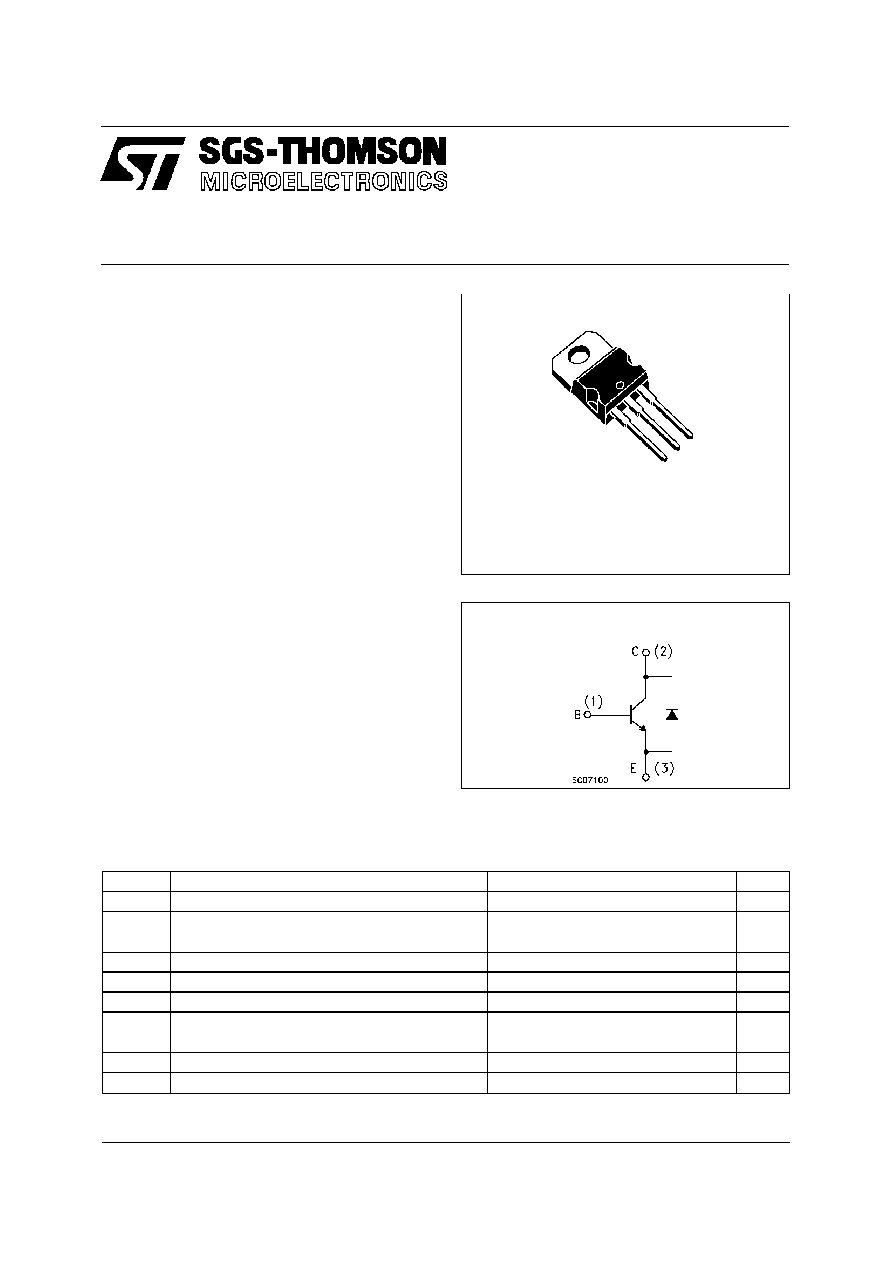
INTERNAL SCHEMATIC DIAGRAM
July 1997
ABSOLUTE MAXIMUM RATINGS
Symbol
Parameter
Val ue
Uni t
V
CES
Collect or-Emitt er Voltage (V
BE
= 0)
800
V
V
CEO
Collect or-Emitt er Voltage (I
B
= 0)
400
V
V
EBO
Emitt er-Base Voltage (I
C
= 0)
9
V
I
C
Collect or Current
5
A
I
CM
Collect or Peak Current (t
p
< 5 ms)
8
A
I
B
Base Current
2
A
I
BM
Base Peak Current (t
p
< 5 ms)
4
A
P
t ot
Total Dissipation at T
c
= 25
o
C
70
W
T
stg
St orage Temperature
-65 to 150
o
C
T
j
Max. Operating Junction Temperature
150
o
C
1
2
3
TO-220
1/6

THERMAL DATA
R
t hj-ca se
R
t hj- amb
Thermal Resistance Junction-Case
Max
Thermal Resistance Junction-Ambient
Max
1.78
62.5
o
C/W
o
C/W
ELECTRICAL CHARACTERISTICS (T
case
= 25
o
C unless otherwise specified)
Symb ol
Parameter
Test Cond ition s
Mi n.
Typ .
Max.
Un it
I
CES
Collect or Cut-off
Current (V
BE
= 0)
V
CE
= 800 V
V
CE
= 800 V
T
j
= 125
o
C
100
500
�
A
�
A
I
CEO
Collect or Cut-off
Current (I
B
= 0)
V
CE
= 400 V
250
�
A
V
CEO (sus)
Collect or-Emitter
Sustaining Voltage
I
C
= 100 mA
L = 25 mH
400
V
V
EBO
Emitt er-Base Voltage
(I
C
= 0)
I
E
= 10 mA
9
V
V
CE(sat )
Collect or-Emitter
Saturat ion Voltage
I
C
= 1 A
I
B
= 0.2 A
I
C
= 2 A
I
B
= 0.4 A
I
C
= 3 A
I
B
= 0.75 A
0.5
0.7
1.1
V
V
V
V
BE(s at)
Base-Emitt er
Saturat ion Voltage
I
C
= 1 A
I
B
= 0.2 A
I
C
= 2 A
I
B
= 0.4 A
1.1
1.2
V
V
h
FE
DC Current G ain
I
C
= 2 A
V
CE
= 5 V
I
C
= 10 mA
V
CE
= 5 V
8
10
t
s
t
s
t
f
RESI STIVE LO AD
St orage Time
St orage Time
Fall T ime
I
C
= 2 A
V
CC
= 250 V t
p
= 30
�
s
I
B1
= 0.4 A
I
B2
= -0.4 V
for BUL381D
for BUL382D
for all
1. 5
2
2.5
3
0.8
�
s
�
s
�
s
t
s
t
f
INDUCTIVE LOAD
St orage Time
Fall T ime
I
C
= 2 A
I
B1
= 0.4 A
V
BE(of f)
= -5 V
R
BB
= 0
V
CL
= 250 V
L = 200
�
H
T
j
= 125
o
C
1.3
100
�
s
�
s
V
f
Diode Forward Volt age
I
C
= 2 A
2.5
V
Pulsed: Pulse duration = 300
�
s, duty cycle 1.5 %
Safe Operating Areas
Derating Curve
BUL381D / BUL382D
2/6

Reverse Biased SOA
Resistive Load Switching Test Ciurcuit
RBSOA and Inductive Load Switching Test
Circuits
1) F ast electronic switch
2) Non-inductive Resist or
3) F ast recovery rectifier
1) Fast electronic switch
2) Non-inductive Resist or
BUL381D / BUL382D
4/6

