 | ÐлекÑÑоннÑй компоненÑ: BULB49DT4 | СкаÑаÑÑ:  PDF PDF  ZIP ZIP |
Äîêóìåíòàöèÿ è îïèñàíèÿ www.docs.chipfind.ru
1/7
September 2003
BULB49D
HIGH VOLTAGE FAST-SWITCHING
NPN POWER TRANSISTOR
s
HIGH VOLTAGE CAPABILITY
s
LOW SPREAD OF DYNAMIC PARAMETERS
s
MINIMUM LOT-TO-LOT SPREAD FOR
RELIABLE OPERATION
s
VERY HIGH SWITCHING SPEED
s
HIGH RUGGEDNESS
s
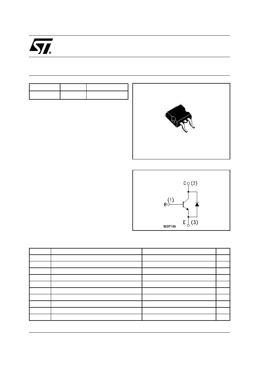
SURFACE MOUNTING TO-263 (D
2
PAK)
POWER PACKAGE IN TAPE & REEL
(SUFFIX "T4")
APPLICATIONS:
s
ELECTRONIC TRANSFORMERS FOR
HALOGEN LAMPS
s
FLYBACK AND FORWARD SINGLE
TRANSISTOR LOW POWER CONVERTERS
DESCRIPTION
The device is manufactured using High Voltage
Multi Epitaxial Planar technology for high switching
speeds and high voltage capability.
The BULB49D is designed for use in electronic
transformers for halogen lamps.
ABSOLUTE MAXIMUM RATINGS
Ordering Code
Marking
Package / Shipment
BULB49DT4
BULB49D
D
2
PAK / Tape & Reel
Symbol
Parameter
Value
Unit
V
CES
Collector-Emitter Voltage (V
BE
= 0)
850
V
V
CEO
Collector-Emitter Voltage (I
B
= 0)
450
V
V
EBO
Emitter-Base Voltage (I
C
= 0, I
B
< 2 A, t
p
< 10 ms)
V
(BR)EBO
V
I
C
Collector Current
5
A
I
CM
Collector Peak Current (t
p
< 5 ms)
10
A
I
B
Base Current
2
A
I
BM
Base Peak Current (t
p
< 5 ms)
4
A
P
tot
Total Dissipation at T
c
= 25 °C
80
W
T
stg
Storage Temperature
65 to 150
°C
T
j
Max. Operating Junction Temperature
150
°C
TO-263
D
2
PAK
(Suffix "T4")
1
3
INTERNAL SCHEMATIC DIAGRAM
BULB49D
2/7
THERMAL DATA
ELECTRICAL CHARACTERISTICS (T
j
= 25 °C unless otherwise specified)
* Pulsed: Pulse duration = 300 µs, duty cycle = 1.5 %.
R
thj-case
R
thj-amb
Thermal Resistance Junction-case
Thermal Resistance Junction-ambient
Max
Max
1.56
62.5
°C/W
°C/W
Symbol
Parameter
Test Conditions
Min.
Typ.
Max.
Unit
I
CES
Collector Cut-off
Current (V
BE
= 0)
V
CE
= 850 V
V
CE
= 850 V
T
j
= 125 °C
100
500
µA
µA
I
EBO
Emitter Cut-off Current
(I
C
= 0)
V
EB
= 9 V
100
µA
V
(BR)EBO
Emitter-Base
Breakdown Voltage
(I
C
= 0)
I
E
= 10 mA
10
18
V
V
CEO(sus)
*
Collector-Emitter
Sustaining Voltage
(I
B
= 0)
I
C
= 10 mA
450
V
V
CE(sat)
*
Collector-Emitter
Saturation Voltage
I
C
= 1 A
I
C
= 2 A
I
C
= 4 A
I
B
= 0.2 A
I
B
= 0.4 A
I
B
= 0.8 A
0.1
0.3
0.6
1.2
V
V
V
V
BE(sat)
*
Base-Emitter
Saturation Voltage
I
C
= 1 A
I
C
= 4 A
I
B
= 0.2 A
I
B
= 0.8 A
1
1.3
V
V
h
FE
*
DC Current Gain
I
C
= 10 mA
I
C
= 500 mA
I
C
= 7 A
V
CE
= 5 V
V
CE
= 5 V
V
CE
= 10 V
10
4
60
10
V
CEW
*
Maximum Collector-
Emitter Voltage
Whithout Snubber
I
C
= 8 A
L = 50 µH
t
p
= 10 µs
V
BB
= -2.5 V
R
BB
= 0
450
V
t
s
t
f
RESISTIVE LOAD
Storage Time
Fall Time
I
C
= 2 A
I
B1
= -I
B2
= 400 mA
(See Figure 1)
V
CC
= 250 V
2
3
0.8
µs
ns
t
s
t
f
INDUCTIVE LOAD
Storage Time
Fall Time
I
C
= 4 A
I
B(on)
= 800 mA
V
BE(off)
= -5 V
(See Figure 2)
V
CL
= 300 V
R
BB(off)
= 0
L = 1 mH
0.6
50
1.3
100
µs
ns
V
f
Diode Forward Voltage
I
C
= 3 A
1.5
V
3/7
BULB49D
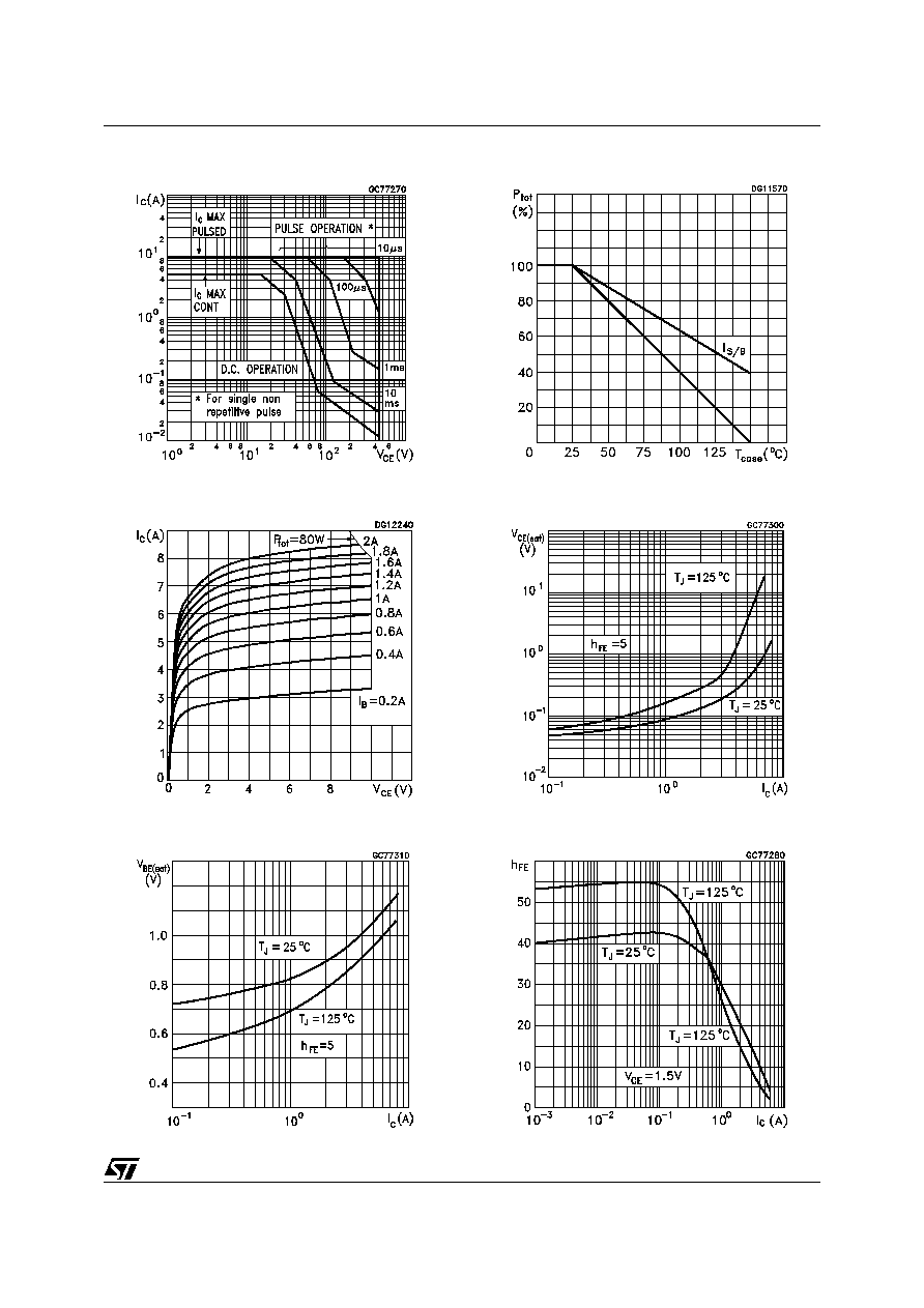
DC Current Gain
Base-Emitter Saturation Voltage
Collector-Emitter Saturation Voltage
Output Characteristics
Safe Operating Area
Derating Curve
BULB49D
4/7
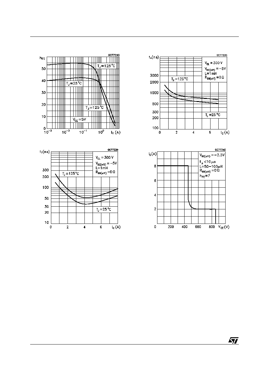
Reverse Biased Safe Operating Area
DC Current Gain
Inductive Load Fall Time
Inductive Load Storage Time
5/7
BULB49D
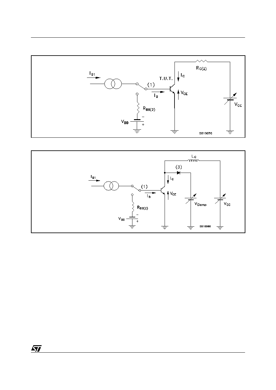
Figure 1: Resistive Load Switching Test Circuit
1) Fast Electronic Switch
2) Non-Inductive Resistor
Figure 2: Inductive Load Switching Test Circuit
1) Fast Electronic Switch
2) Non-Inductive Resistor
3) Fast Recovery Rectifier