 | –≠–ª–µ–∫—Ç—Ä–æ–Ω–Ω—ã–π –∫–æ–º–ø–æ–Ω–µ–Ω—Ç: BULT118 | –°–∫–∞—á–∞—Ç—å:  PDF PDF  ZIP ZIP |
BULT118
HIGH VOLTAGE FAST-SWITCHING
NPN POWER TRANSISTORS
s
STMicroelectronics PREFERRED
SALESTYPE
s
NPN TRANSISTOR
s
HIGH VOLTAGE CAPABILITY
s
LOW SPREAD OF DYNAMIC PARAMETERS
s
MINIMUM LOT-TO-LOT SPREAD FOR
RELIABLE OPERATION
s
VERY HIGH SWITCHING SPEED
APPLICATIONS:
s
ELECTRONIC BALLASTS FOR
FLUORESCENT LIGHTING
s
FLYBACK AND FORWARD SINGLE
TRANSISTOR LOW POWER CONVERTERS
DESCRIPTION
The device is manufactured using high voltage
Multi
Epitaxial
Planar
technology
for
high
switching speeds and medium voltage capability.
It uses a Cellular Emitter structure with planar
edge termination to enhance switching speeds
while maintaining the wide RBSOA.
The device is designed for use in lighting
applications and low cost switch-mode power
supplies.
Æ
INTERNAL SCHEMATIC DIAGRAM
June 2000
ABSOLUTE MAXIMUM RATINGS
Symbol
Parameter
Val ue
Uni t
V
CES
Collect or-Emitt er Voltage (V
BE
= 0)
700
V
V
CEO
Collect or-Emitt er Voltage (I
B
= 0)
400
V
V
EBO
Emitt er-Base Voltage (I
C
= 0)
9
V
I
C
Collect or Current
2
A
I
CM
Collect or Peak Current (t
p
< 5 ms)
4
A
I
B
Base Current
1
A
I
BM
Base Peak Current (t
p
< 5 ms)
2
A
P
t ot
Total Dissipation at T
c
= 25
o
C
45
W
T
stg
St orage Temperature
-65 to 150
o
C
T
j
Max. Operating Junction Temperature
150
o
C
3
2
1
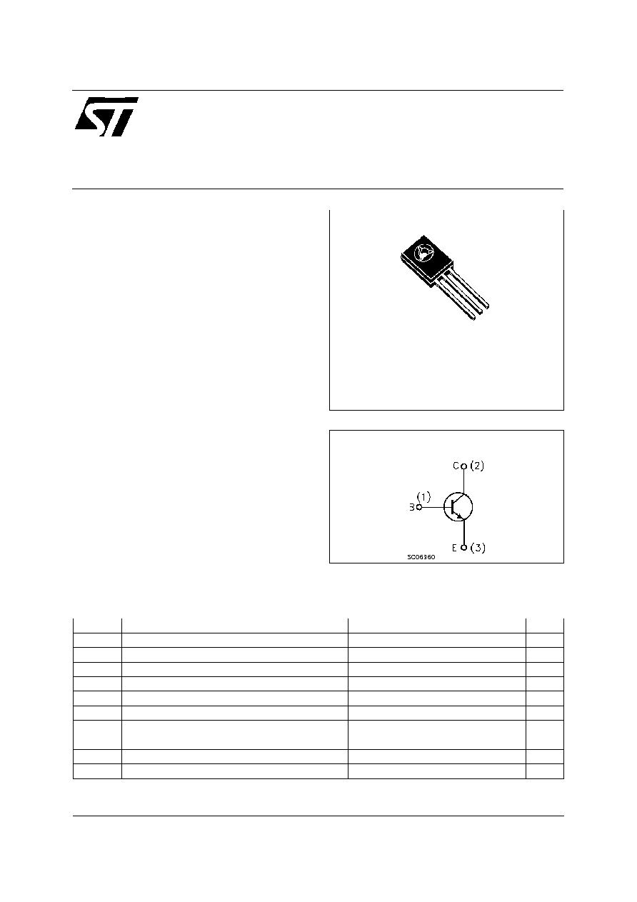
SOT-32
1/7

THERMAL DATA
R
t hj-ca se
R
t hj- amb
Thermal Resistance Junction-Case
Max
Thermal Resistance Junction-Ambient
Max
2.77
80
o
C/W
o
C/W
ELECTRICAL CHARACTERISTICS (T
case
= 25
o
C unless otherwise specified)
Symb ol
Parameter
Test Cond ition s
Mi n.
Typ .
Max.
Un it
I
CES
Collect or Cut-off
Current (V
BE
= 0)
V
CE
= 700 V
V
CE
= 700 V
T
j
= 125
o
C
100
500
µ
A
µ
A
V
EBO
Emitt er-Base Voltage
I
E
= 10 mA
9
V
V
CEO(sus )
Collect or-Emitter
Sustaining Voltage
(I
B
= 0)
I
C
= 100 mA
L = 25 mH
400
V
I
CEO
Collect or-Emitter
Leakage Current
V
CE
= 400 V
250
µ
A
V
CE(sat )
Collect or-Emitter
Saturat ion Voltage
I
C
= 0. 5 A
I
B
= 0.1 A
I
C
= 1 A
I
B
= 0.2 A
I
C
= 2 A
I
B
= 0.4 A
0.5
1
1.5
V
V
V
V
BE(s at)
Base-Emitt er
Saturat ion Voltage
I
C
= 0. 5 A
I
B
= 0.1 A
I
C
= 1 A
I
B
= 0.2 A
I
C
= 2 A
I
B
= 0.4 A
1.0
1.2
1.3
V
V
V
h
FE
DC Current G ain
I
C
= 10 mA
V
CE
= 5 V
I
C
= 0. 5 A
V
CE
= 5 V
I
C
= 2 A
V
CE
= 5 V
10
10
8
50
t
r
t
s
t
f
RESI STIVE LO AD
Rise Time
St orage Time
Fall T ime
V
CC
= 125 V
I
C
= 1 A
I
B1
= 0.2 A
I
B2
= -0.2 A
0.4
3.2
0. 25
0.7
4.5
0.4
µ
s
µ
s
µ
s
t
s
t
f
INDUCTIVE LOAD
St orage Time
Fall T ime
I
C
= 1 A
I
B1
= 0.2 A
V
BE
= -5 V
L = 50 mH
V
c la mp
= 300 V
0.8
0. 16
µ
s
µ
s
Pulsed: Pulse duration = 300 ms, duty cycle 1.5 %
BULT118
2/7
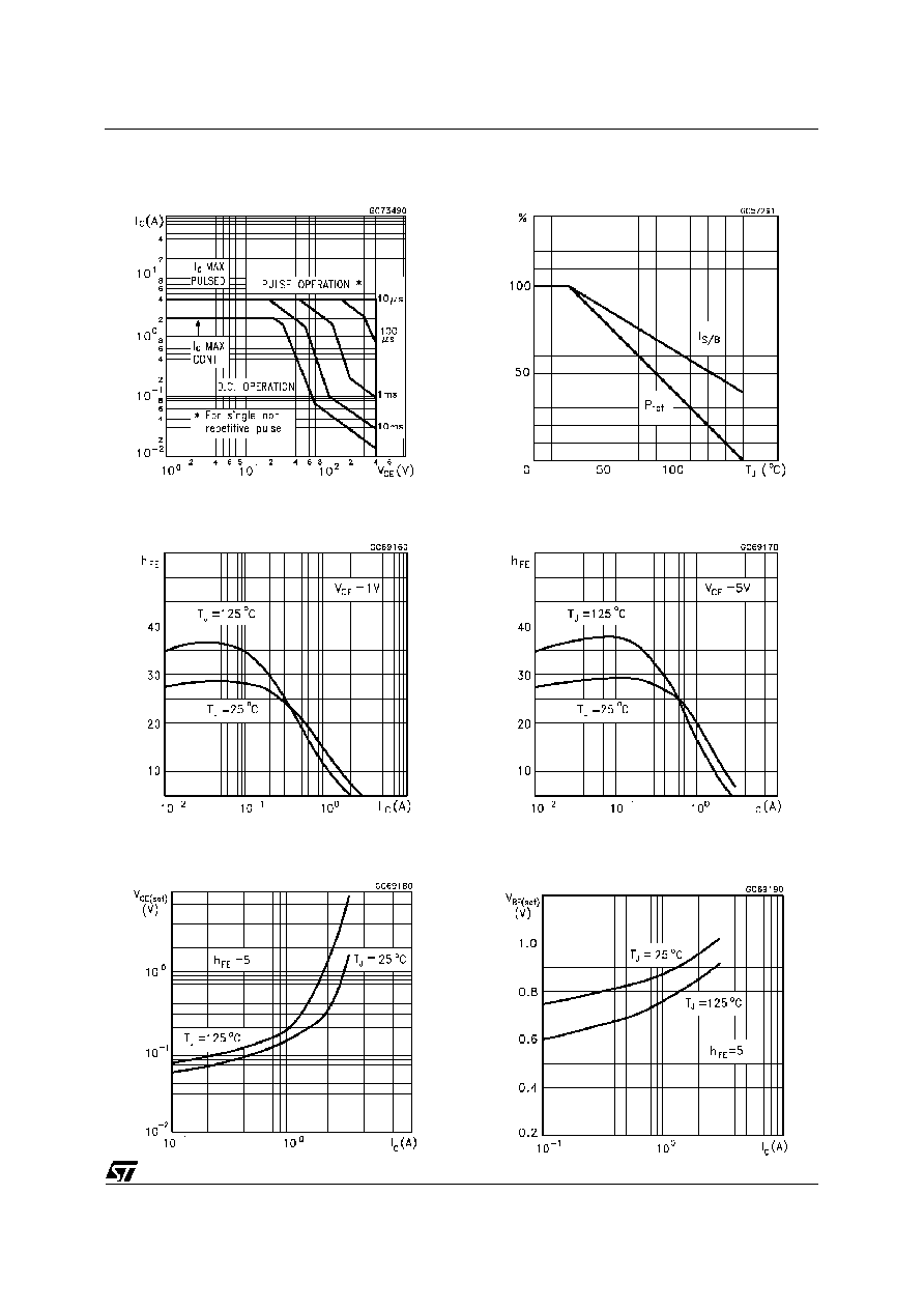
Safe Operating Areas
DC Current Gain
Collector Emitter Saturation Voltage
Derating Curve
DC Current Gain
Base Emitter Saturation Voltage
BULT118
3/7
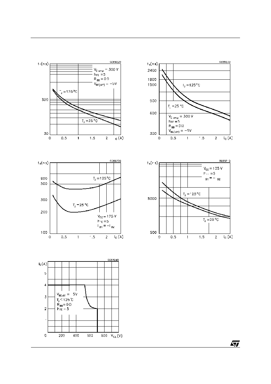
Inductive Fall Time
Inductive Storage Time
Resistive Fall Time
Resistive Load Storage Time
Reverse Biased SOA
BULT118
4/7

Figure 1: Inductive Load Switching Test Circuits.
Figure 2: Resistive Load Switching Test Circuits.
1) Fast electronic switch
2) Non-inductive Resist or
3) Fast recovery rectifier
1) Fast electronic switch
2) Non-inductive Resist or
BULT118
5/7