 | –≠–ª–µ–∫—Ç—Ä–æ–Ω–Ω—ã–π –∫–æ–º–ø–æ–Ω–µ–Ω—Ç: BUR51 | –°–∫–∞—á–∞—Ç—å:  PDF PDF  ZIP ZIP |
BUR51
HIGH CURRENT NPN SILICON TRANSISTOR
s
SGS-THOMSON PREFERRED SALESTYPE
s
NPN TRANSISTOR
DESCRIPTION
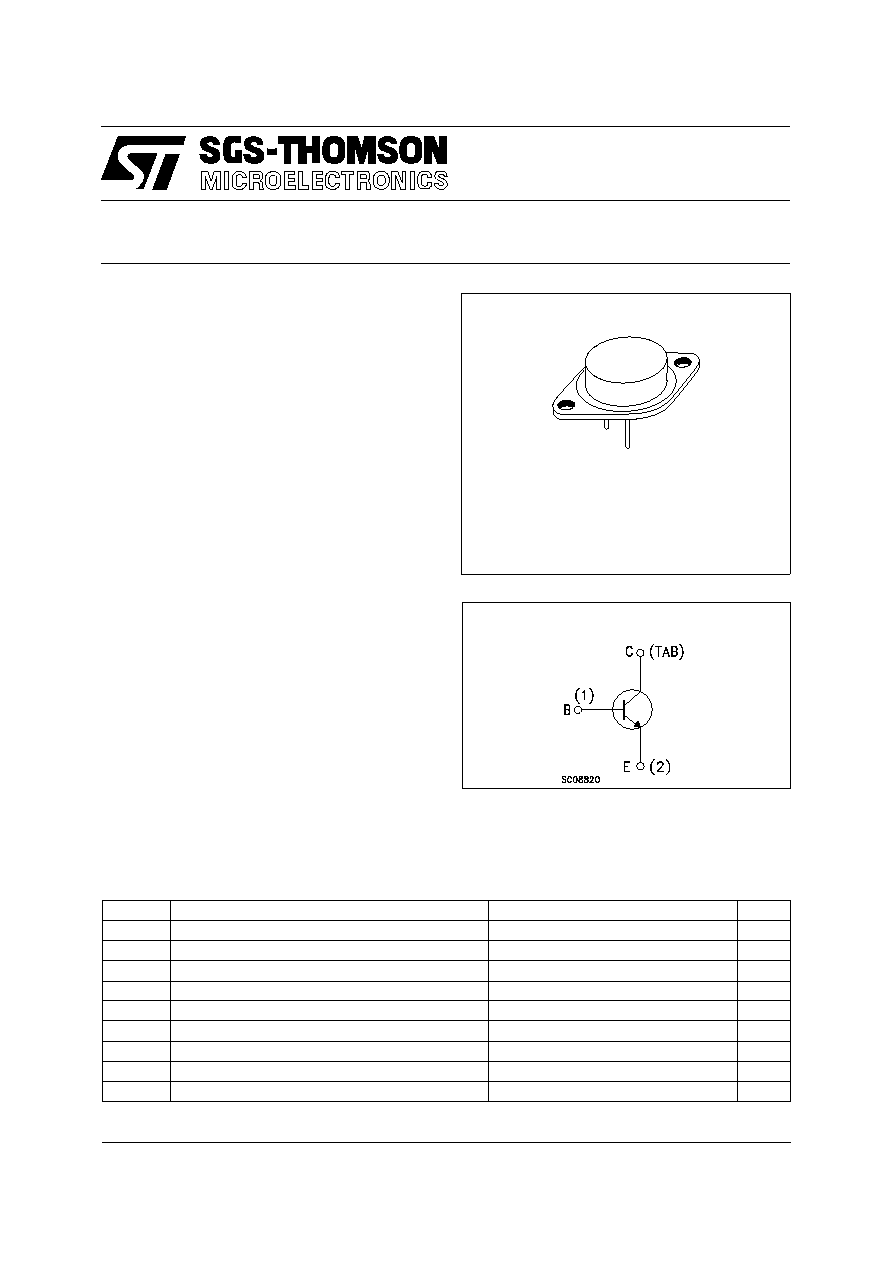
The BUR51 is a silicon multiepitaxial planar NPN
transistor in modified Jedec TO-3 metal case,
intented for use in switching and linear
applications in military and industrial equipment.
INTERNAL SCHEMATIC DIAGRAM
June 1997
1
2
TO-3
ABSOLUTE MAXIMUM RATINGS
Symbol
Parameter
Value
Unit
V
CBO
Collector-Base Voltage (I
E
= 0)
300
V
V
CEO
Collector-Emitter Voltage (I
B
= 0)
200
V
V
EBO
Emitter-Base Voltage (I
C
= 0)
10
V
I
C
Collector Current
60
A
I
CM
Collector Peak Current (t
p
= 10 ms)
80
A
I
B
Base Current
16
A
P
tot
Total Dissipation at T
c
25
o
C
350
W
T
stg
Storage Temperature
-65 to 200
o
C
T
j
Max. Operating Junction Temperature
200
o
C
1/4
THERMAL DATA
R
thj-case
Thermal Resistance Junction-case Max
0.5
o
C/W
ELECTRICAL CHARACTERISTICS (T
case
= 25
o
C unless otherwise specified)
Symbol
Parameter
Test Conditions
Min.
Typ.
Max.
Unit
I
CBO
Collector Cut-off
Current (I
E
= 0)
V
CB
= 300 V
V
CB
= 300 V T
case
= 125
o
C
0.2
2
mA
mA
I
CEO
Collector Cut-off
Current (I
B
= 0)
V
CE
=200 V
1
mA
I
EBO
Emitter Cut-off Current
(I
C
= 0)
V
EB
= 7 V
0.2
µ
A
V
CEO(sus)
Collector-Emitter
Sustaining Voltage
I
C
= 200 mA
200
V
V
EBO
Emitter-base Voltage
(I
C
= 0)
I
E
= 10 mA
10
V
V
CE(sat)
Collector-emitter
Saturation Voltage
I
C
= 30 A I
B
= 2 A
I
C
= 50 A I
B
= 5 A
0.9
1
1.5
V
V
V
BE(sat)
Base-emitter
Saturation Voltage
I
C
= 30 A I
B
= 2 A
I
C
= 50 A I
B
= 5 A
1.55
1.8
2
V
V
h
FE
DC Current Gain
I
C
= 5 A V
CE
= 4 V
I
C
= 50 A V
CE
= 4 V
20
15
100
I
s/b
Second Breakdown
Collector Current
V
CE
= 20 V t = 1 s
17.5
A
f
T
Transition-Frequency
I
C
= 1 A V
CE
= 5 V
f = 1 MHz
10
16
MHz
t
on
Turn-on Time
IC = 50 A I
B1
= 5 A
V
CC
= 100 V
0.35
1
µ
s
t
s
Storage Time
IC = 50 A I
B1
= 5 A
I
B2
= -5 A V
CC
= 100 V
0.9
2
µ
s
t
f
Fall Time
0.24
0.6
µ
s
Clamped E
s/b
Collector
Current
V
clamp
= 200 V L = 500
µ
H
50
A
Pulsed: Pulse duration = 300
µ
s, duty cycle 1.5 %
BUR51
2/4
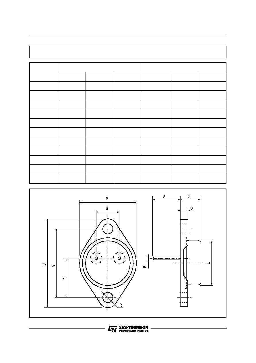
DIM.
mm
inch
MIN.
TYP.
MAX.
MIN.
TYP.
MAX.
A
11
11.7
13.1
0.433
0.461
0.516
B
1.45
1.5
1.6
0.057
0.059
0.063
C
2.7
2.92
0.106
0.115
D
8.9
9.4
0.350
0.370
E
19
20
0.748
0.787
G
10.7
10.9 11.1
0.421
0.429
0.437
N
16.5
16.9 17.2
0.650
0.665
0.677
P
25
26
0.984
1.024
R
3.88
4.2
0.153
0.165
U
38.5
39.3
1.516
1.547
V
30
30.14
30.3
1.181
1.187
1.193
P003I
TO-3 (I) MECHANICAL DATA
BUR51
3/4

Information furnished is believed to be accurate and reliable. However, SGS-THOMSON Microelectronics assumes no responsability for the
consequences of use of such information nor for any infringement of patents or other rights of third parties which may results from its use. No
license is granted by implication or otherwise under any patent or patent rights of SGS-THOMSON Microelectronics. Specifications mentioned
in this publication are subject to change without notice. This publication supersedes and replaces all information previously supplied.
SGS-THOMSON Microelectronics products are not authorized for use as critical components in life support devices or systems without express
written approval of SGS-THOMSON Microelectonics.
© 1997 SGS-THOMSON Microelectronics - Printed in Italy - All Rights Reserved
SGS-THOMSON Microelectronics GROUP OF COMPANIES
Australia - Brazil - Canada - China - France - Germany - Hong Kong - Italy - Japan - Korea - Malaysia - Malta - Morocco - The Netherlands -
Singapore - Spain - Sweden - Switzerland - Taiwan - Thailand - United Kingdom - U.S.A
. . .
BUR51
4/4