 | –≠–ª–µ–∫—Ç—Ä–æ–Ω–Ω—ã–π –∫–æ–º–ø–æ–Ω–µ–Ω—Ç: BYT01-400 | –°–∫–∞—á–∞—Ç—å:  PDF PDF  ZIP ZIP |

Æ
BYT 01-400
FAST RECOVERY RECTIFIER DIODES
FAST RECOVERY RECTIFIER
VERY LOW REVERSE RECOVERY TIME
VERY LOW SWITCHING LOSSES
LOW NOISE TURN-OFF SWITCHING
SUITABLE APPLICATION
FREE WHEELING DIODE IN CONVERTERS
AND MOTORS CIRCUITS
RECTIFIER IN S.M.P.S.
October 1999 Ed : 1A
F 126
(Plastic)
Symbol
Parameter
Value
Unit
I
FRM
Repetive Peak Forward Current
t
p
10
µ
s
30
A
I
F (AV)
Average Forward Current*
T
a
= 70
∞
C
= 0.5
1
A
I
FSM
Surge non Repetitive Forward Current
t
p
= 10ms
Sinusoidal
30
A
P
Power Dissipation*
Ta = 70
∞
C
1.33
W
T
stg
T
j
Storage and Junction Temperature Range
- 40 to +150
- 40 to + 150
∞
C
ABSOLUTE RATINGS (limiting values)
Symbol
Parameter
Value
Unit
R
th (j - a)
Junction-ambient*
60
∞
C/W
THERMAL RESISTANCE
Symbol
Parameter
Value
Unit
V
RRM
Repetitive Peak Reverse Voltage
400
V
V
RSM
Non Repetitive Peak Reverse Voltage
440
V
* On infinite heatsink with 10mm lead length.
1/5
2/5
Symbol
Test Conditions
Min.
Typ.
Max.
Unit
I
R
T
j
= 25
∞
C
V
R
= V
RRM
20
µ
A
T
j
= 100
∞
C
0.5
mA
V
F
T
j
= 25
∞
C
I
F
= 1A
1.5
V
T
j
= 100
∞
C
1.4
STATIC CHARACTERISTICS
ELECTRICAL CHARACTERISTICS
Symbol
Test Conditions
Min.
Typ.
Max.
Unit
t
rr
T
j
= 25
∞
C
I
F
= 1A di
F
/dt = - 15A/
µ
s V
R
= 30V
55
ns
T
j
= 25
∞
C
I
F
= 0.5A I
R
= 1A
I
rr
= 0.25A
25
RECOVERY CHARACTERISTICS
To evaluate the conduction losses use the following equations:
V
F
= 1.05 + 0.145 I
F
P = 1.05 x I
F(AV)
+ 0.145 I
F
2
(RMS)
Symbol
Test Conditions
Min.
Typ.
Max.
Unit
t
IRM
di
F
/dt = - 50A/
µ
s
T
j
= 100
∞
C V
CC
= 200 V I
F
= 1A
35
50
ns
I
RM
di
F
/dt = - 50A/
µ
s
L
p
0.05
µ
A See figure 12
1.5
2
A
TURN-OFF SWITCHING CHARACTERISTICS (Without Series inductance)
BYT 01-400
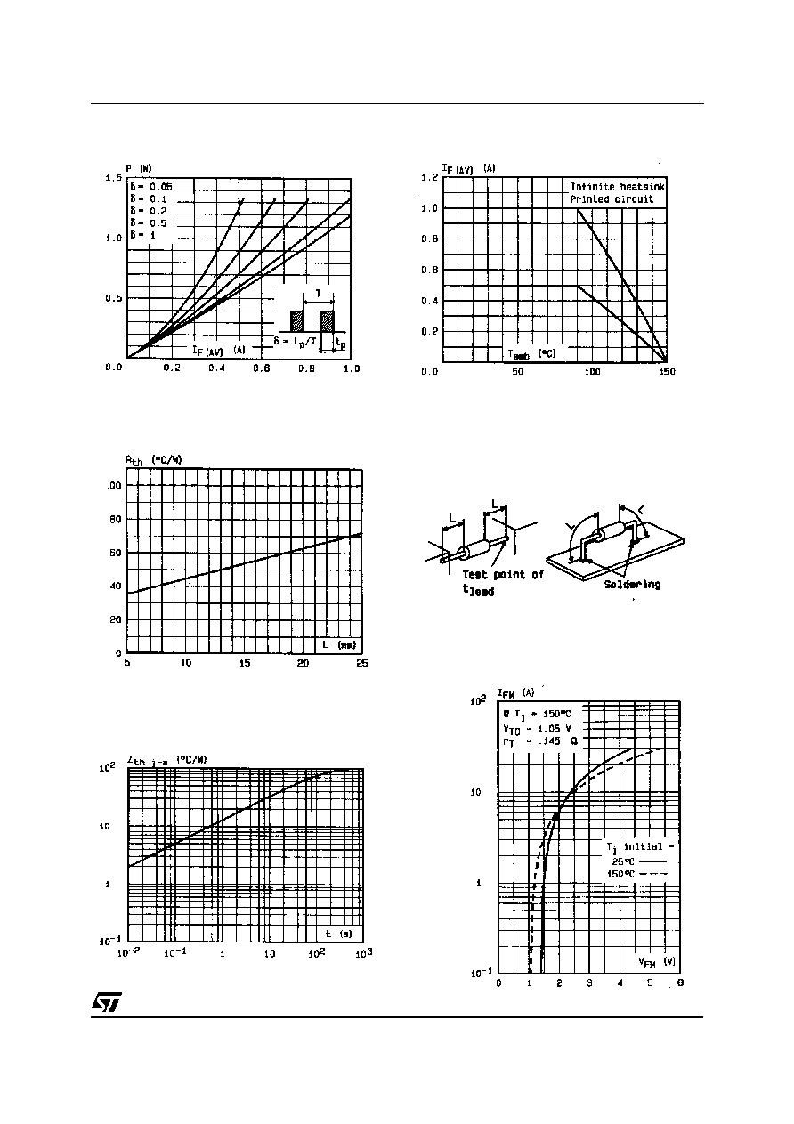
Figure 2. Average forward current versus
ambient temperature.
Figure 3. Thermal resistance versus lead
length.
Figure 4. Transient thermal impedance
junction-ambient for mounting n∞2 versus
pulse duration (L = 10 mm).
Figure 5. Peak forward current
versus peak forward voltage drop
(maximum values).
Mounting n∞1
INFINITE HEATSINK
Mounting n∞2
PRINTED CIRCUIT
Fi g ur e 1. M a xi mu m av erag e po wer
dissipation versus average forward current.
3/5
BYT 01-400

4/5
Figure 7. Recovery time versus di
F
/dt.
Figure 8. Peak forward voltage versus di
F
/dt.
Figure 9. Peak reverse current versus di
F
/dt.
Figure 11. Dynamic parameters versus
junction temperature.
Figure 10. Recovered charge versus di
F
/dt
(typical values).
Figure 12. Non repetitive surge peak current
versus number of cycles.
BYT 01-400

F 126 (Plastic)
PACKAGE MECHANICAL DATA
Marking: type number
Cooling method: by convection (method A)
Weight: 0.393g
REF.
DIMENSIONS
Millimeters
Inches
Min.
Typ.
Max.
Min.
Typ.
Max.
A
6.05
6.20
6.35 0.238 0.244 0.250
B
2.95
3.00
3.05
0.116 0.118 0.120
C
26
31
1.024
1.220
D
0.76
0.81
0.86 0.030 0.032 0.034
A
C
C
D
D
B
Information furnished is believed to be accurate and reliable. However, STMicroelectronics assumes no responsibility for the consequences
of use of such information nor for any infringement of patents or other rights of third parties which may result from its use. No license is granted
by implication or otherwise under any patent or patent rights of STMicroelectronics. Specifications mentioned in this publication are subject to
change without notice. This publication supersedes and replaces all information previously supplied.
STMicroelectronics products are not authorized for use as critical components in life support devices or systems without express written approval
of STMicroelectronics.
The ST logo is a registered trademark of STMicroelectronics
© 1999 STMicroelectronics - Printed in Italy - All rights reserved.
STMicroelectronics GROUP OF COMPANIES
Australia - Brazil - China - Finland - France - Germany - Hong Kong - India - Italy - Japan - Malaysia
Malta - Morocco - Singapore - Spain - Sweden - Switzerland - United Kingdom - U.S.A.
http://www.st.com
5/5
BYT 01-400