 | –≠–ª–µ–∫—Ç—Ä–æ–Ω–Ω—ã–π –∫–æ–º–ø–æ–Ω–µ–Ω—Ç: BZW04-13 | –°–∫–∞—á–∞—Ç—å:  PDF PDF  ZIP ZIP |

1/6
BZW04-5V8/376
BZW04-5V8B/376B
TRANSIL
TM
s
PEAK PULSE POWER : 400 W (10/1000
µ
s)
s
STAND-OFF VOLTAGE RANGE :
From 5.8V to 376 V
s
UNI AND BIDIRECTIONAL TYPES
s
LOW CLAMPING FACTOR
s
FAST RESPONSE TIME
s
UL RECOGNIZED
FEATURES
DO-15
Symbol
Parameter
Value
Unit
P
PP
Peak pulse power dissipation (see note 1)
Tj initial = Tamb
400
W
P
Power dissipation on infinite heatsink
T
amb
= 75∞C
1.7
W
I
FSM
Non repetitive surge peak forward current
for unidirectional types
tp = 10ms
Tj initial = T
amb
30
A
T
stg
T
j
Storage temperature range
Maximum junction temperature
- 65 to + 175
175
∞C
∞
C
T
L
Maximum lead temperature for soldering during 10s a 5mm
from case.
230
∞
C
Note 1 : For a surge greater than the maximum values, the diode will fail in short-circuit.
ABSOLUTE MAXIMUM RATINGS (T
amb
= 25∞C)
DESCRIPTION
Transil diodes provide high overvoltage protection
by clamping action. Their instantaneous response
to transient overvoltages makes them particu-
larly suited to protect voltage sensitive devices
such as MOS Technology and low voltage sup-
plied IC's.
February 2003- Ed : 3A
Symbol
Parameter
Value
Unit
R
th (j-l)
Junction to leads
60
∞C/W
R
th (j-a)
Junction to ambient on printed circuit.
L
lead
= 10 mm
100
∞
C/W
THERMAL RESISTANCES
Æ

BZW04-xx
2/6
I
I F
V F
V
VCL
VBR
VRM
I PP
I RM
V
Symbol
Parameter
V
RM
Stand-off voltage
V
BR
Breakdown voltage
V
CL
Clamping voltage
I
RM
Leakage current @ V
RM
I
PP
Peak pulse current
T
Voltage temperature coefficient
V
F
Forward voltage drop
ELECTRICAL CHARACTERISTICS (T
amb
= 25∞C)
Types
I
RM
@ V
RM
V
BR
@
I
R
V
CL
@ I
PP
V
CL
@ I
PP
T
C
max
min
max
max
max
typ
note2
10/1000
µ
s
8/20
µ
s
note3
note4
Unidirectional
Bidirectional
µ
A
V
V
mA
V
A
V
A
10
-4
/∞C
pF
BZW04-5V8
BZW04-5V8B
1000
5.8
6.45
10
10.5
38.0
13.4
174
5.7
3500
BZW04-6V4
BZW04-6V4B
500
6.4
7.13
10
11.3
35.4
14.5
160
6.1
3100
BZW04-8V5
BZW04-8V5B
10
8.5
9.5
1
14.5
27.6
18.6
124
7.3
2000
BZW04-10
BZW04-10B
5
10.2
11.4
1
16.7
24.0
21.7
106
7.8
1550
BZW04-13
BZW04-13B
5
12.8
14.3
1
21.2
19.0
27.2
85
8.4
1200
BZW04-15
BZW04-15B
1
15.3
17.1
1
25.2
16.0
32.5
71
8.8
975
BZW04-19
BZW04-19B
1
18.8
20.9
1
30.6
13.0
39.3
59
9.2
800
BZW04-20
BZW04-20B
1
20.5
22.8
1
33.2
12.0
42.8
54
9.4
725
BZW04-23
BZW04-23B
1
23.1
25.7
1
37.5
10.7
48.3
48
9.6
625
BZW04-26
BZW04-26B
1
25.6
28.5
1
41.5
9.6
53.5
43
9.7
575
BZW04-28
BZW04-28B
1
28.2
31.4
1
45.7
8.8
59.0
39
9.8
510
BZW04-31
BZW04-31B
1
30.8
34.2
1
49.9
8.0
64.3
36
9.6
480
BZW04-33
BZW04-33B
1
33.3
37.1
1
53.9
7.4
69.7
33
10.0
450
BZW04-40
BZW04-40B
1
40.2
44.7
1
64.8
6.2
84
27
10.1
370
BZW04-48
BZW04-48B
1
47.8
53.2
1
77.0
5.2
100
23
10.3
320
BZW04-58
BZW04-58B
1
58.1
64.6
1
92.0
4.3
121
19
10.4
270
BZW04-70
BZW04-70B
1
70.1
77.9
1
113
3.5
146
16.0
10.5
230
BZW04-85
BZW04-85B
1
85.5
95.0
1
137
2.9
178
13.0
10.6
200
BZW04-102
BZW04-102B
1
102
114
1
165
2.4
212
11.0
10.7
170
BZW04-128
BZW04-128B
1
128
143
1
207
2.0
265
9.0
10.8
145
BZW04-154
BZW04-154B
1
154
171
1
246
1.6
317
7.0
10.8
125
BZW04-171
BZW04-171B
1
171
190
1
274
1.5
353
6.5
10.8
120
BZW04-188
BZW04-188B
1
188
209
1
328
1.4
388
6.0
10.8
110
BZW04-213
BZW04-213B
1
231
237
1
344
1.5
442
5.2
11.0
100
BZW04-256
BZW04-256B
1
256
285
1
414
1.2
529
4.3
11.0
90
BZW04-xx
3/6
Types
I
RM
@ V
RM
V
BR
@
I
R
V
CL
@ I
PP
V
CL
@ I
PP
T
C
min
max
max
max
typ
note2
10/1000
µ
s
8/20
µ
s
note3
note4
Unidirectional
Bidirectional
µ
A
V
V
mA
V
A
V
A
10
-4
/∞C
pF
BZW04-273
BZW04-273B
1
273
304
1
438
1.2
564
4.0
11.0
85
BZW04-299
BZW04-299B
1
299
332
1
482
0.9
618
3.7
11.0
80
BZW04-342
BZW04-342B
1
342
380
1
548
0.9
706
3.2
11.0
75
BZW04-376
BZW04-376B
1
376
418
1
603
0.8
776
3.0
11.0
70
Note 2 :
Pulse test: tp < 50 ms.
Note 3 :
VBR =
T * (Tamb - 25) * VBR(25∞C)
Note 4 :
VR = 0 V, F = 1 MHz. For bidirectional types,
capacitance value is divided by 2
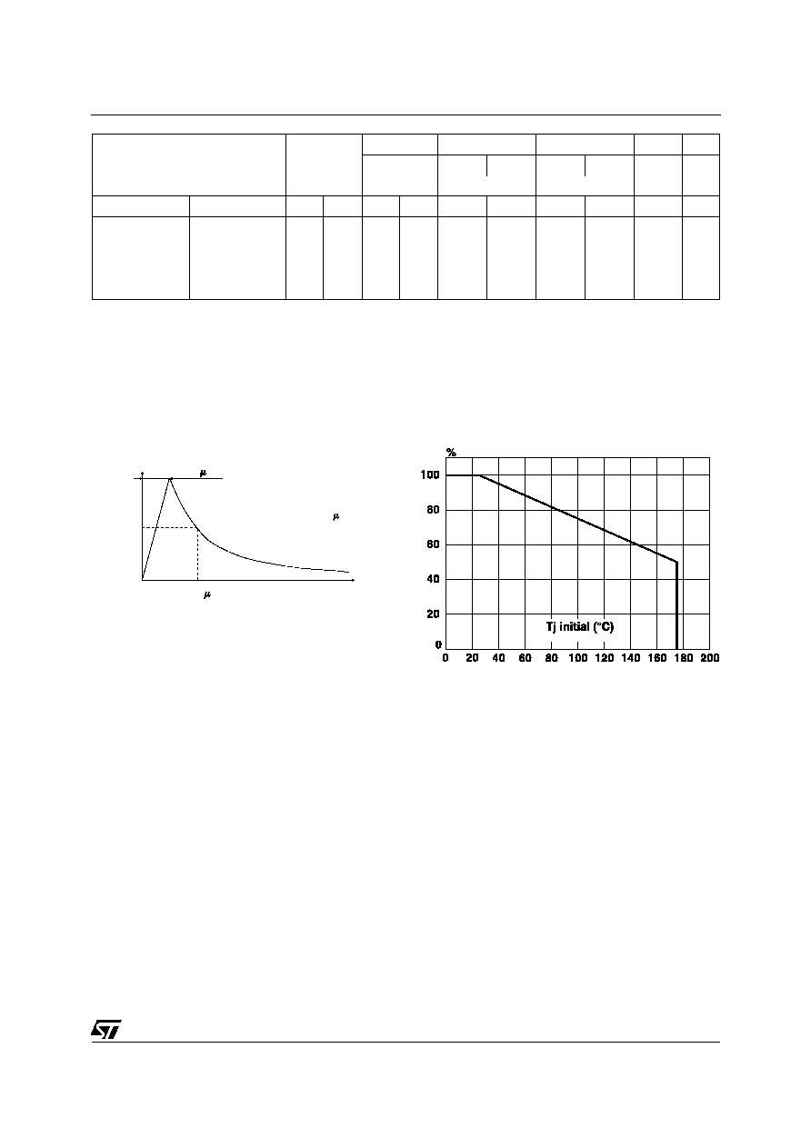
Fig. 1: Peak pulse power dissipation versus initial
junction temperature (printed circuit board).
10 s
1000 s
% I
PP
50
0
t
PULSE WAVEFORM 10/1000
s
100

BZW04-xx
4/6
0.001
0.01
0.1
1
10
100
tp (ms ) EXPO.
1E3
1E2
1E1
1E5
1E4
P
(W)
PP
Tj initial = 25∞C
Fig. 2 : Peak pulse power versus exponential pulse duration.
0.1
1
10
100
1000
1
10
100
1000
10
100
BWZ04 5V8
BWZ04 8V5
BWZ04 33
BWZ04 213
BWZ04 376
V
(V)
CL
Ipp (A)
t
% Ipp
100
50
0
t r
t < 10
s
r
t
-
-
-
-
-
Tj initial = 25∞C
Fig. 3 : Clamping voltage versus peak pulse current.
Exponential waveform t
p
= 20
µ
s________
t
p
= 1 ms-------------
t
p
= 10 ms...............
Note : The curves of the figure 3 are specified for a junction temperature of 25∞C before surge.
The given results may be extrapolated for other junction temperatures by using the following formula :
V
BR
=
T
*
(T
amb
-25)
*
V
BR
(25∞C).
For intermediate voltages, extrapolate the given results.
BZW04-xx
5/6
0.01
0.1
1
10
100
1000
1
10
100
Zth (j-a) ( C/W)
∞
tp(s)
Fig. 6: Transient thermal impedance junction ambi-
ent versus pulse duration (For FR4 PC Board
with L
lead
= 10mm).
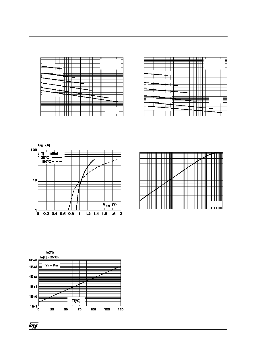
Fig. 5: Peak forward voltage drop versus peak forward
current (typical values for unidirectional types).
Note : Multiply by 2 for units with VBR > 220V.
C (pF)
1
10
100
10
100
1000
10000
BZW04 - 13B
BZW04 - 5V8B
BZW04 - 58B
BZW04 - 171B
BZW04 - 342B
BZW04 - 26B
V
(V)
R
Tj = 25¯C
f = 1 MHz
∞
Fig. 4b: Capacitance versus reverse applied
voltage for bidirectional types (typical values).
C (pF)
1
10
100
1
10
100
1000
10000
BZW04 13
BZW04 5V8
BZW04 58
BZW04 171
BZW04 342
BZW04 26
V
(V)
R
Tj = 25¯C
f = 1 MHz
-
-
-
-
-
-
Fig. 4a: Capacitance versus reverse applied
voltage for unidirectional types (typical values).
Fig. 7 : Relative variation of leakage current
versus junction temperature.