
1/6
BZW06-5V8/376
BZW06-5V8B/376B
TRANSIL
TM
s
PEAK PULSE POWER : 600 W (10/1000
µ
s)
s
STAND-OFF VOLTAGE RANGE :
From 5.8V to 376 V
s
UNI AND BIDIRECTIONAL TYPES
s
LOW CLAMPING FACTOR
s
FAST RESPONSE TIME
s
UL RECOGNIZED
FEATURES
DO-15
Symbol
Parameter
Value
Unit
P
PP
Peak pulse power dissipation (see note 1)
Tj initial = Tamb
600
W
P
Power dissipation on infinite heatsink
T
amb
= 75∞C
1.7
W
I
FSM
Non repetitive surge peak forward current
for unidirectional types
tp = 10ms
Tj initial = T
amb
100
A
T
stg
T
j
Storage temperature range
Maximum junction temperature
- 65 to + 175
175
∞
C
∞
C
T
L
Maximum lead temperature for soldering during 10s a 5mm
from case.
230
∞C
Note 1 : For a surge greater than the maximum values, the diode will fail in short-circuit.
ABSOLUTE MAXIMUM RATINGS (T
amb
= 25∞C)
DESCRIPTION
Transil diodes provide high overvoltage protection
by clamping action. Their instantaneous response
to transient overvoltages makes them particu-
larly suited to protect voltage sensitive devices
such as MOS Technology and low voltage sup-
plied IC's.
February 2003 - Ed : 3A
Symbol
Parameter
Value
Unit
R
th (j-l)
Junction to leads
60
∞C/W
R
th (j-a)
Junction to ambient on printed circuit.
L
lead
= 10 mm
100
∞
C/W
THERMAL RESISTANCES
Æ
BZW06-xx
3/6
Types
I
RM
@ V
RM
V
BR
@
I
R
V
CL
@ I
PP
V
CL
@ I
PP
T
C
min
max
max
max
typ
note2
10/1000
µ
s
8/20
µ
s
note3
note4
Unidirectional
Bidirectional
µ
A
V
V
mA
V
A
V
A
10
-4
/∞C
pF
BZW06-188
BZW06-188B
1
188
209
1
328
2.0
388
10.3
10.8
330
BZW06-213
BZW06-213B
1
231
237
1
344
2.0
442
9.0
11.0
310
BZW06-256
BZW06-256B
1
256
285
1
414
1.6
529
7.6
11.0
290
BZW06-273
BZW06-273B
1
273
304
1
438
1.6
564
7.1
11.0
280
BZW06-299
BZW06-299B
1
299
332
1
482
1.6
618
6.5
11.0
270
BZW06-342
BZW06-342B
1
342
380
1
548
1.3
706
5.7
11.0
360
BZW06-376
BZW06-376B
1
376
418
1
603
1.3
776
5.7
11.0
350
Note 2 :
Pulse test: tp < 50 ms.
Note 3 :
VBR =
T * (Tamb - 25) * VBR(25∞C)
Note 4 :
VR = 0 V, F = 1 MHz. For bidirectional types,
capacitance value is divided by 2
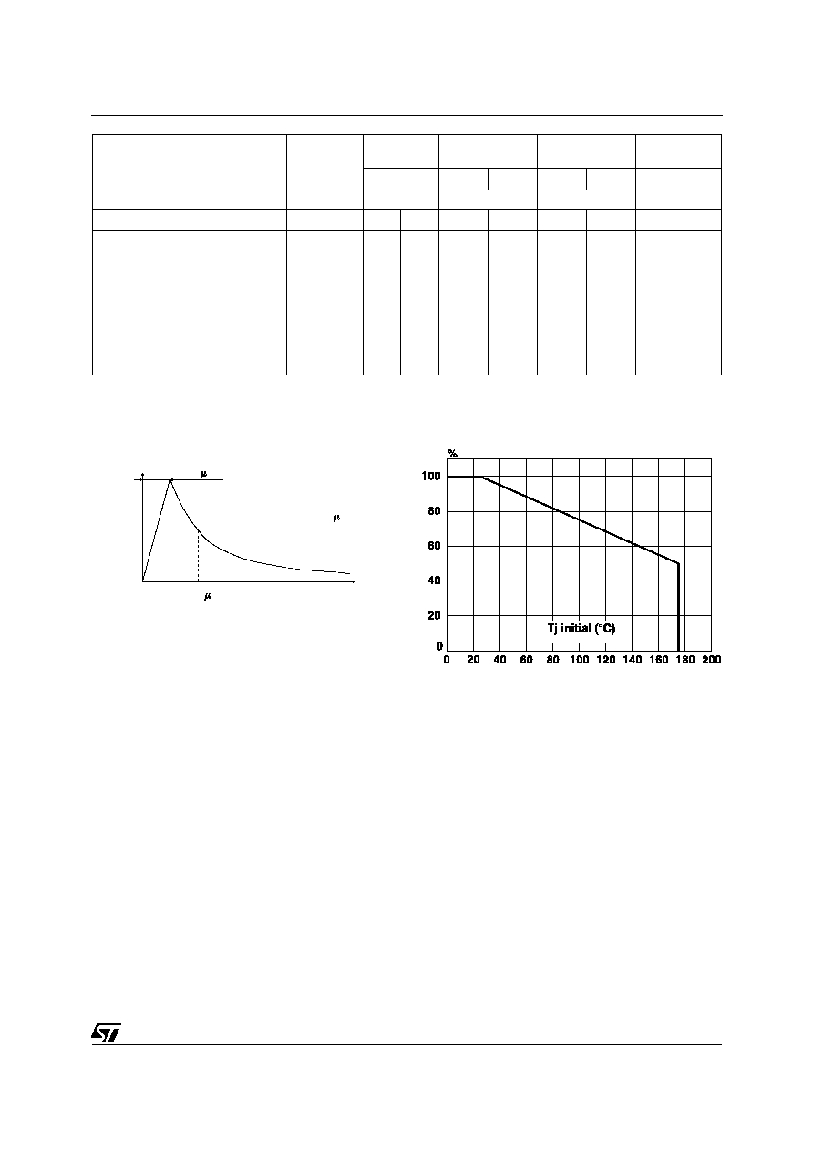
Fig. 1: Peak pulse power dissipation versus initial
junction temperature (printed circuit board).
10 s
1000 s
% I
PP
50
0
t
PULSE WAVEFORM 10/1000
s
100
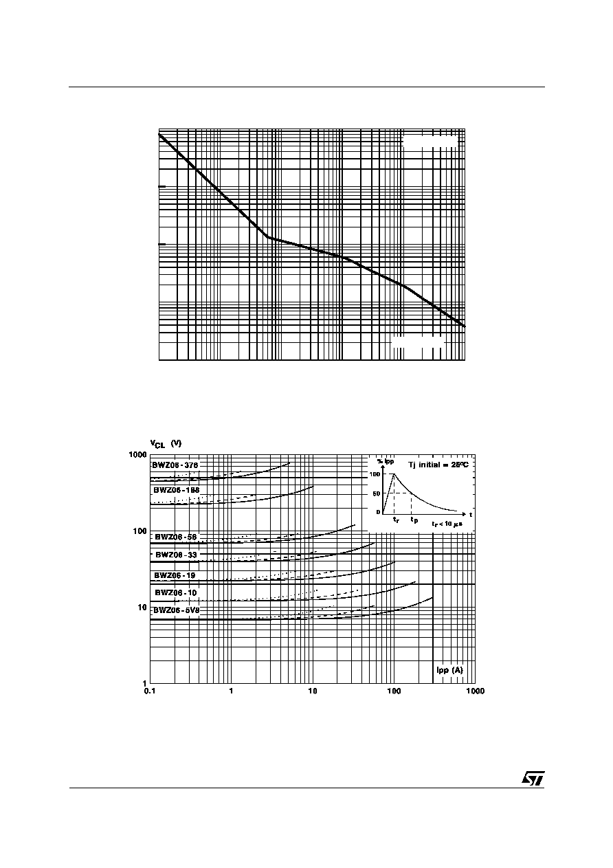
BZW06-xx
4/6
0.001
0.01
0.1
1
10
100
1E1
1E2
1E3
1E4
1E5
tp (m
S
) EXPO.
Tj initial = 25¯C
Ppp (W)
∞
Fig. 2 : Peak pulse power versus exponential pulse duration.
Fig. 3 : Clamping voltage versus peak pulse current.
Exponential waveform t
p
= 20
µ
s________
t
p
= 1 ms-------------
t
p
= 10 m...............
Note : The curves of the figure 3 are specified for a junction temperature of 25∞C before surge.
The given results may be extrapolated for other junction temperatures by using the following formula :
V
BR
=
T
*
(T
amb
-25)
*
V
BR
(25∞C).
For intermediate voltages, extrapolate the given results.
BZW06-xx
5/6
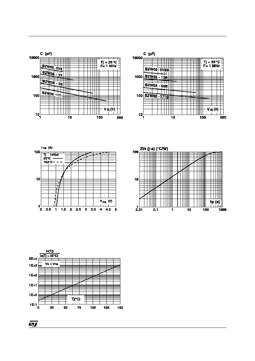
Fig. 6 : Transient thermal impedance junction ambi-
ent versus pulse duration (For FR4 PC Board
with L
lead
= 10mm).
Fig. 5 : Peak forward voltage drop versus peak for-
ward current (typical values for unidirectional
types).
Fig. 4b : Capacitance versus reverse applied
voltage for bidirectional types (typical values).
Fig. 4a : Capacitance versus reverse applied
voltage for unidirectional types (typical values).
Fig. 7 : Relative variation of leakage current ver-
sus junction temperature.
