Äîêóìåíòàöèÿ è îïèñàíèÿ www.docs.chipfind.ru
®
1/7
MAIN PRODUCT CHARACTERISTICS
Where EMI filtering in ESD sensitive equipment is
required:
Mobile phones and communication systems
Computers, printers and MCU Boards
DESCRIPTION
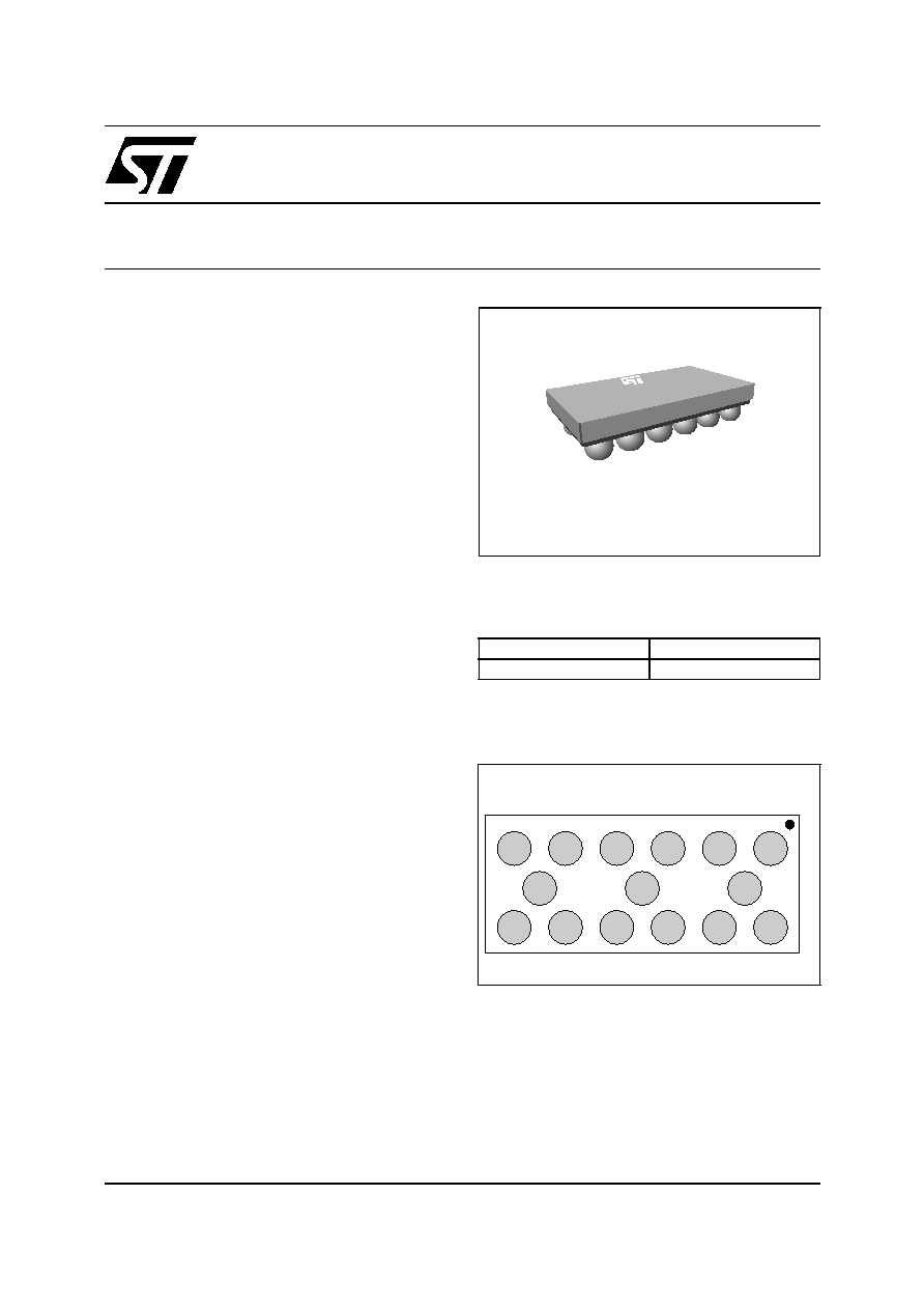
The EMIF04-10006F2 is a highly integrated
devices designed to suppress EMI/RFI noise in all
systems subjected to electromagnetic
interferences. The EMIF04 flip-chip packaging
means the package size is equal to the die size.
This filter includes an ESD protection circuitry
which prevents the device from destruction when
subjected to ESD surges up 15kV. This device
includes four EMIF filters and 4 separated ESD
diodes.
BENEFITS
EMI symmetrical (I/O) low-pass filter
High efficiency in EMI filtering
Lead free package
Very low PCB space consuming:
2.92mm x 1.29mm
Very thin package: 0.65 mm
High efficiency in ESD suppression
(IEC61000-4-2 level 4)
High reliability offered by monolithic integration
High reducing of parasitic elements through
integration and wafer level packaging.
COMPLIES WITH THE FOLLOWING STANDARDS:
IEC 61000-4-2 level 4:
15kV (air discharge)
8kV
(contact discharge)
MIL STD 883E - Method 3015-6 Class 3: 30kV
EMIF04-10006F2
4 LINES EMI FILTER
AND ESD PROTECTION
REV. 1
®
Flip-Chip
(15 Bumps)
September 2004
Figure 1: Pin Configuration (ball side)
I3
O3
D1
D2
D3
Gnd
Gnd
Gnd
D4
I2
O2
I4
O4
I1
O1
9
8
7
6
5
4
3
2
1
A
B
C
IPADTM
TM: IPAD is a trademark of STMicroelectronics.
Table 1: Order Code
Part Number
Marking
EMIF04-10006F2
FS
EMIF04-10006F2
2/7
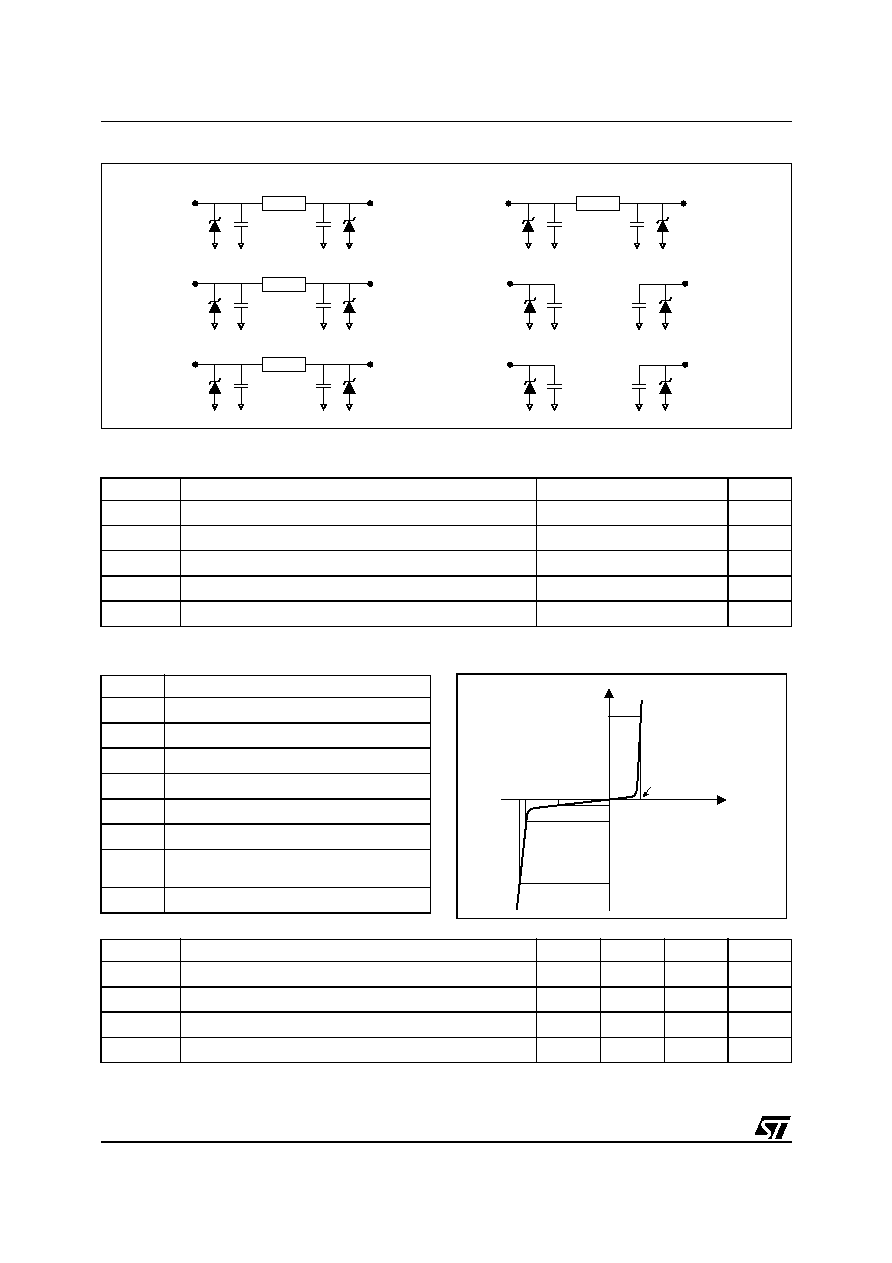
Figure 2: Basic Cell Configuration
Table 2: Absolute Ratings (limiting values)
Table 3: Electrical Characteristics (T
amb
= 25 °C)
Symbol
Parameter and test conditions
Value
Unit
P
R
DC power per resistance
0.1
W
P
T
Total DC power per package
0.6
W
T
j
Maximum junction temperature
125
°C
T
op
Operating temperature range
- 40 to + 85
°C
T
stg
Storage temperature range
125
°C
Symbol
Parameter
V
BR
Breakdown voltage
I
RM
Leakage current @ V
RM
V
RM
Stand-off voltage
V
CL
Clamping voltage
R
d
Dynamic impedance
I
PP
Peak pulse current
R
I/O
Series resistance between Input
and output
C
line
Capacitance per line
Symbol
Test conditions
Min.
Typ.
Max.
Unit
V
BR
I
R
= 1 mA
5.5
7
9
V
I
RM
V
RM
= 3.3 V per line
500
nA
R
I/O
I = 10 mA
80 100 120
C
line
V
R
= 2.5 V, F = 1 MHz, 30 mV (on filter cells)
50
60
70
pF
Output 4
Input 1
30pF
30pF
100
Output 1
Input 4
30pF
30pF
100
D1
D2
30pF
30pF
D3
D4
30pF
30pF
Input 2
30pF
30pF
100
Output 2
Input 3
30pF
30pF
100
Output 3
I
V
I
F
V
F
I
RM
I
R
I
PP
V
RM
V
BR
V
CL
EMIF04-10006F2
3/7
Figure 3: S21 (dB) attenuation measurements
and Aplac simulation
Figure 4: Analog crosstalk measurements
Figure 5: Digital crosstalk measurements
Figure 6: ESD response to IEC61000-4-2 (+15kV
air discharge) on one imput V(in) and one output
V(out)
Figure 7: ESD response to IEC61000-4-2 (15kV
air discharge) on one imput V(in) and one output
V(out)
Figure 8: Line capacitance versus applied
voltage for filter
100.0k
1.0M
10.0M
100.0M
1.0G
-50.00
-37.50
-25.00
-12.50
0.00
dB
f/Hz
Simulation
Measurement
100.0k
1.0M
10.0M
100.0M
1.0G
-50.00
-37.50
-25.00
-12.50
0.00
dB
f/Hz
Simulation
Measurement
Simulation
Measurement
Aplac 7.62 User: ST Microelectronics
100k
1M
10M
100M
1G
00
-25
-50
-75
-100
Aplac 7.62 User: ST Microelectronics
dB
dB
i3_o2.s2p
f/Hz
0
10
20
30
40
50
60
70
80
90
100
0.0
0.5
1.0
1.5
2.0
2.5
3.0
3.5
4.0
4.5
5.0
V (V)
R
C(pF)
F=1MHz
V
osc
=30mV
RMS
T
j
=25°C
EMIF04-10006F2
4/7
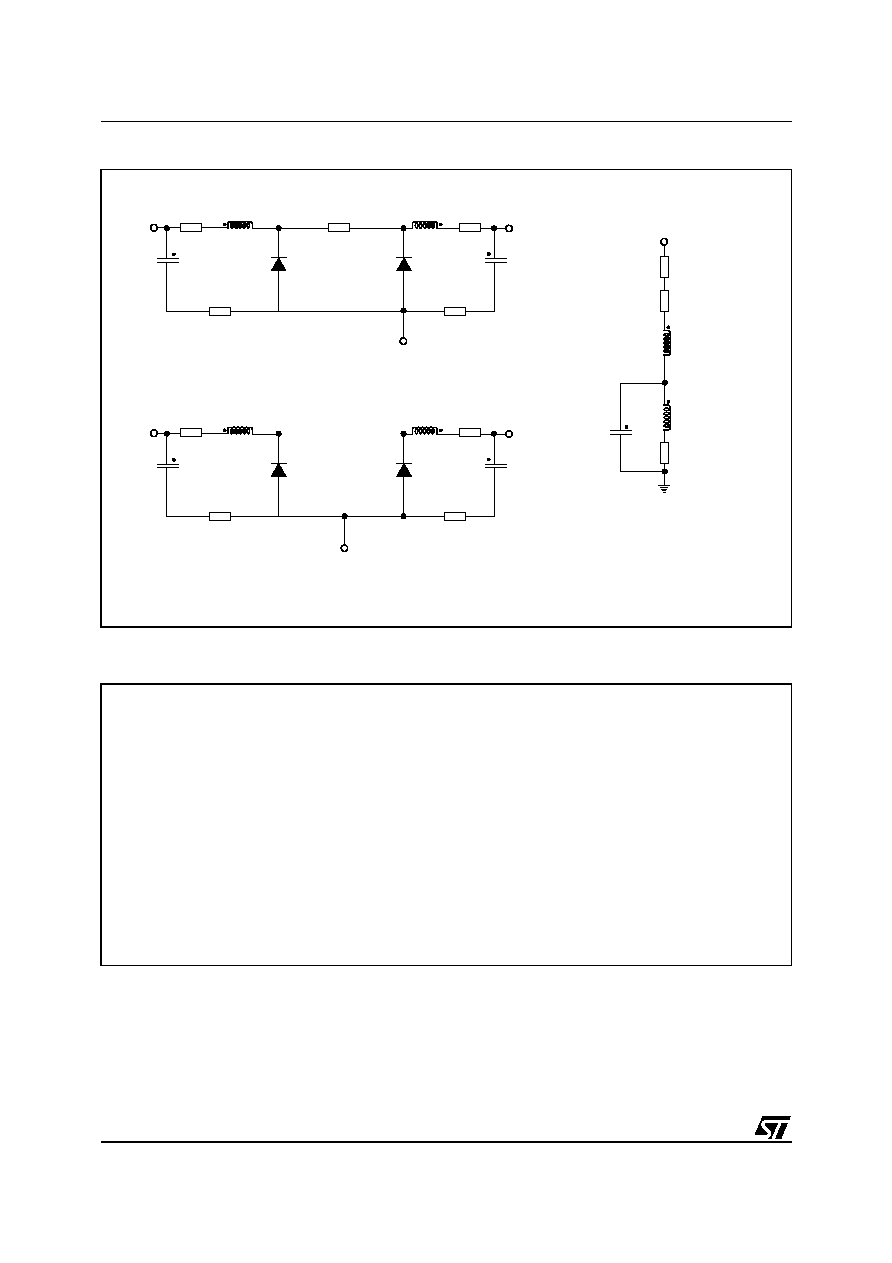
Figure 9: Aplac model
Figure 10: Aplac parameters
EMIF04-10006F2 model
Ground return for each GND bump
Oi * = Output of each filter cell
Ii* = Input of each filter cell
Oi*
Cz=41pF@0V
Cz=41pF@0V
sub
Rs=100
Lbump
Rbump
Rsub
Cbump
Ii*
Rsub
Lbump
Rbump
Cbump
Di*
Cz=41pF@0V
Cz=41pF@0V
sub
Lbump
Rbump
Rsub
Cbump
Dj *
Rsub
Lbump
Rbump
Cbump
With Dj* = D1 & D3
And Di* = D2 & D4
sub
Lbump
Rbump
sub
Rsub
Lgnd
Rgnd
Cgnd
Cgnd
Cgnd
aplacvar RS
aplacvar Cz
aplacvar Lbump
aplacvar Rbump
aplacvar Cbump
aplacvar Rsub
aplacvar Rgnd
aplacvar Lgnd
aplacvar Cgnd
100
41 pF
50 pH
20 m
1.2 pF
100 m
100 m
100 pH
0.15 pF
EMIF04-10006F2
5/7
Figure 11: Order code
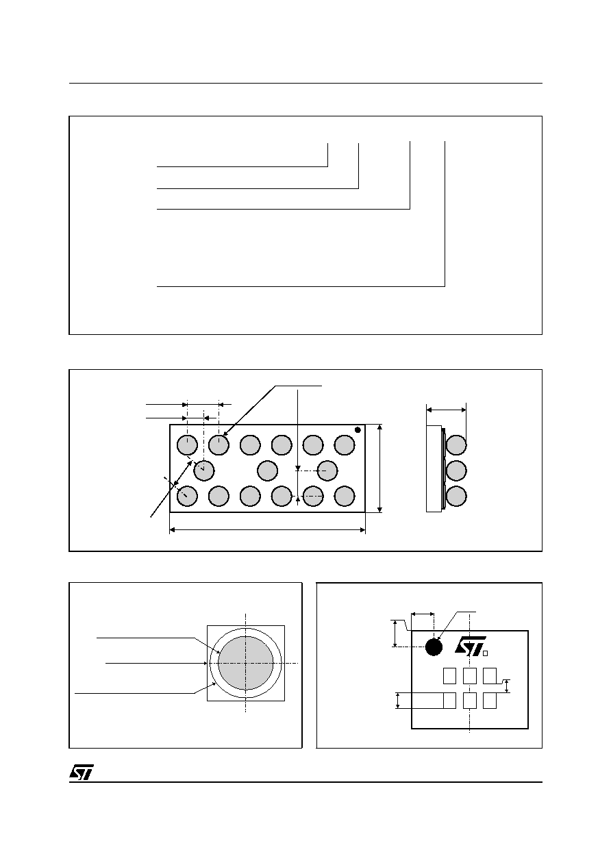
Figure 12: FLIP-CHIP Package Mechanical Data
Figure 13: Foot print recommendations
Figure 14: Marking
EMIF yy - xxx zz Fx
EMI Filter
Number of lines
Information
Package
x = resistance value (Ohms)
z = capacitance value / 10(pF)
or
3 letters = application
2 digits = version
F = Flip-Chip
x
= 1: 500µm, Bump = 315µm
= 2: Leadfree Pitch = 500µm, Bump = 315µm
2.92mm ± 50µm
1.29mm ± 50µm
435µm ± 50
315µm ± 50
501µm
±
50
500µm ± 50
250µm ± 50
650µm ± 65
Copper pad Diameter :
250µm recommended , 300µm max
Solder stencil opening : 330µm
Solder mask opening recommendation :
340µm min for 300µm copper pad diameter
545
545
400
100
230
x
y
z
w
x
w
Dot, ST logo
xx = marking
yww = datecode
(y = year
ww = week)
z = packaging
location
All dimensions in µm
E