1/9
ESDA6V1-5W6
TRANSIL
TM
ARRAY
FOR ESD PROTECTION
Æ
DESCRIPTION
The ESDA6V1-5W6 is a 5-bit wide monolithic
suppressor
which
is
designed
to
protect
components connected to data and transmission
lines against ESD.
March 2000 - Ed: 1A
Where transient overvoltage protection in ESD
sensitive equipment is required, such as :
n
Computers
n
Printers
n
Communication systems
n
Cellular phone handsets and accessories
n
Other telephone sets
n
Set top boxes
APPLICATIONS
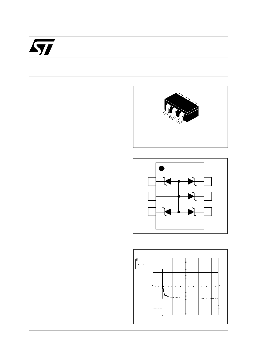
SOT323-6L
I/O1
I/O2
Gnd
I/O5
I/O3
I/O4
FUNCTIONAL DIAGRAM
Application Specific Di
scretes
A.S.D.
‰
BENEFITS
n
High integration
n
Suitable for high density boards
- IEC 61000-4-2: level 4
15 kV
(air discharge)
8 kV
(contact discharge)
- MIL STD 883C-Method 3015-6: class3
(human body model)
COMPLIES WITH THE FOLLOWING STANDARDS:
n
5 UNIDIRECTIONAL TRANSIL
TM
FUNCTIONS
n
BREAKDOWN VOLTAGE: VBR = 6.1V min
n
LOW LEAKAGE CURRENT: I
R
max < 1
µ
A
n
VERY SMALL SIZE FOR PCB SPACE SAVING:
4.2mm
2
TYPICALLY
FEATURES
ESD response to IEC61000-4-2
(air discharge 16kV, positive surge)

ESDA6V1-5W6
2/9
Symbol
Test conditions
Value
Unit
V
PP
ESD discharge - MIL STD 883C - Method 3015-6
IEC 61000-4-2 air discharge
IEC 61000-4-2 contact discharge
25
20
15
kV
P
PP
Peak pulse power (8/20
µ
s)
100
W
T
j
Junction temperature
150
∞C
T
stg
Storage temperature range
-55 to +150
∞C
T
L
Lead solder temperature (10 seconds duration)
260
∞
C
T
op
Operating temperature range (note 1)
-40 to +125
∞C
Note 1: The evolution of the operating parameters versus temperature is given by curves and
T parameter.
ABSOLUTE MAXIMUM RATINGS (T
amb
= 25∞C)
V
cl
V
BR
V
RM
Slope = 1/Rd
V
F
I
F
I
RM
I
PP
I
V
Type
V
BR
@ I
R
I
RM
@ V
RM
Rd
T
C
V
F
@ I
F
min.
max
.
max.
typ.
max.
typ.
max
note 2
note 3
0V bias
V
V
mA
µ
A
V
m
10
-4
/∞C
pF
V
mA
ESDA6V1-5W6
6.1
7.2
1
1
3
610
6
50
1.25
200
Note 2 : Square pulse, Ipp = 15A, tp=2.5
µ
s.
Note 3:
VBR =
T * (Tamb - 25∞C) * VBR (25∞C)
Symbol
Parameter
V
RM
Stand-off voltage
V
BR
Breakdown voltage
V
CL
Clamping voltage
I
RM
Leakage current
I
PP
Peak pulse current
T
Voltage temperature coefficient
C
Capacitance
Rd
Dynamic impedance
V
F
Forward voltage drop
ELECTRICAL CHARACTERISTICS (T
amb
= 25∞C)

ESDA6V1-5W6
3/9
0
25
50
75
100
125
150
175
0.0
0.1
0.2
0.3
0.4
0.5
0.6
0.7
0.8
0.9
1.0
1.1
Tj initial(∞C)
Ppp[Tj initial]/Ppp[Tj initial=25∞C]
Fig. 1: Peak power dissipation versus initial
junction temperature.
1
10
100
10
100
1000
tp(µs)
Ppp(W)
Fig. 2: Peak pulse power versus exponential
pulse duration (Tj initial = 25∞C).
0
5
10
15
20
25
30
35
40
0.1
1.0
10.0
50.0
Vcl(V)
Ipp(A)
tp=2.5µs
Fig. 3: Clamping voltage versus peak pulse current
(Tj initial = 25∞C) Rectangular waveform tp = 2.5
µ
s.
0.5
1.0
1.5
2.0
2.5
3.0
3.5
4.0
4.5
5.0
10
20
30
40
50
VR(V)
C(pF)
F=1MHz
Vosc=30mV
Fig. 4: Capacitance versus reverse applied voltage
(typical values).
25
50
75
100
125
1
10
50
Tj(∞C)
IR[Tj] / IR[Tj=25∞C]
Fig. 5: Relative variation of leakage current ver-
sus junction temperature (typical values).
0.6
0.7
0.8
0.9
1.0
1.1
1.2
1.3
1.4
1.5
1.6
1E-3
1E-2
1E-1
1E+0
VFM(V)
IFM(A)
Tj=25∞C
Fig. 6: Peak forward voltage drop versus peak
forward current (typical values).

4/9
ESDA6V1-5W6
I
C
t
o
be pr
ot
ect
e
d
C
onnect
o
r
Implementation of ESDA6V1-5W6 in a typical application
APPLICATION EXAMPLE
TECHNICAL INFORMATION
The ESDA6V1-5W6 is particularly optimized to perform ESD protection. ESD protection is achieved by
clamping the unwanted overvoltage. The clamping voltage is given by the following formula :
V
V
R I
cl
br
d
pp
=
+
As shown in figure A1, the ESD strikes are clamped by the transient voltage suppressor.
ESD PROTECTION
ESD Surge
Voutput
Rload
Rg
Rd
Vbr
Vg
Device
to be
protected
ESDA6V1-5W6
Fig. A1: ESD clamping behavior

ESDA6V1-5W6
5/9
To have a good approximation of the remaining voltages at both Vi/o side, we provide the typical dynamical
resistance value Rd. By taking into account the following hypothesis :
Rg > Rd and Rload > Rd
we have:
Vin
V
R
V
R
br
d
g
g
=
+
◊
The results of the calculation done for Vg = 8 kV, Rg = 330
(IEC 61000-4-2 standard), Vbr = 6.4 V (typ.)
and Rd = 0.61
(typ.) give:
Vouput = 21.2 V
This confirms the very low remaining voltage across the device to be protected. It is also important to note
that in this approximation the parasitic inductance effect was not taken into account. This could be a few
tenths of volts during a few ns at the Vi/o side.
TEST BOARD
ESD
SURGE
16kV
Air
Discharge
Vi/o
E62
Fig. A2: Measurement conditions: