
HCC/HCF40100B
32-STAGE STATIC LEFT/RIGHT SHIFT REGISTER
DESCRIPTION
.
FULLY STATIC OPERATION
.
SHIFT LEFT/SHIFT RIGHT CAPABILITY
.
MULTIPLE PACKAGE CASCADING
.
RECIRCULATE CAPABILITY
.
LIFO OR FIFO CAPABILITY
.
STANDARDIZED
SYMMETRICAL
OUTPUT
CHARACTERISTICS
.
QUIESCENT CURRENT SPECIFIED AT 20V
FOR HCC DEVICE
.
5V, 10V, AND 15V PARAMETRIC RATINGS
.
INPUT CURRENT OF 100nA AT 18V AND 25
∞
C
FOR HCC DEVICE
.
100% TESTED FOR QUIESCENT CURRENT
.
MEETS ALL REQUIREMENTS OF JEDEC TEN-
TATIVE STANDARD N
o
. 13A, "STANDARD
SPECIFICATIONS FOR DESCRIPTION OF "B"
SERIES CMOS DEVICES"
June 1989
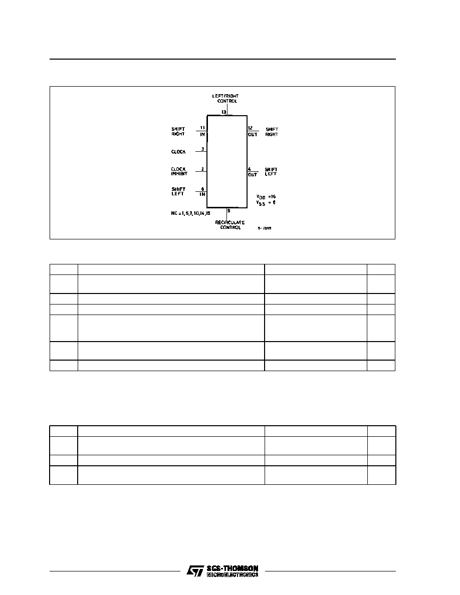
The HCC40100B (extended temperature range)
and HCF40100B (intermediate temperature range)
are monolithic integrated circuits, available in 16-
lead dual in-line plastic or ceramic package and
plastic micro package. The HCC/HCF40100B is a
32-stage shift register containing 32 D-type master-
slave flip-flops. The data present at the SHIFT-
RIGHT INPUT is transferred into the first register
stage synchronously with the positive CLOCK edge,
provided the LEFT/RIGHT CONTROL is at a low
level, the RECIRCULATE CONTROL is at a high
level, and the CLOCK INHIBIT is low. If the
LEFT/RIGHT CONTROL is at a high level and the
RECIRCULATE CONTROL is also high, data at the
SHIFT-LEFT INPUT is transferred into the 32nd reg-
ister stage synchronously with the positive CLOCK
transition, provided the CLOCK INHIBIT is low. The
state of the LEFT/RIGHT CONTROL, RECIRCU-
LATE CONTROL, and CLOCK INHIBIT should not
be changed when the CLOCK is high. Data is shifted
one stage left or one stage right depending on the
state of the LEFT/RIGHT CONTROL, synchron-
ously with the positive CLOCK edge. Data clocked
into the first or 32nd register states is available at the
SHIFT-LEFT or SHIFT-RIGHT OUTPUT respec-
tively, on the next negative CLOCK transition (see
Data Transfer Table). No shifting occurs on the posi-
tive CLOCK edge if the CLOCK INHIBIT line is at a
high level. With the RECIRCULATE CONTROL low,
EY
(Plastic Package)
C1
(Plastic Chip Carrier)
ORDER CODES :
HCC40100BF
HCF40100BM1
HCF40100BEY
HCF40100BC1
PIN CONNECTIONS
data in the 32nd stage is shifted into the first stage
when the LEFT/RIGHT CONTROL is low and from
the 1st stage to the 32nd stage when the
LEFT/RIGHT CONTROL is high.
M1
(Micro Package)
F
(Ceramic Frit Seal Package)
1/13
FUNCTIONAL DIAGRAM
ABSOLUTE MAXIMUM RATINGS
Symbol
Parameter
Value
Unit
V
DD
*
Supply Voltage : HC C Types
H C F Types
≠ 0.5 to + 20
≠ 0.5 to + 18
V
V
V
i
Input Voltage
≠ 0.5 to V
DD
+ 0.5
V
I
I
DC Input Current (any one input)
±
10
mA
P
t o t
Total Power Dissipation (per package)
Dissipation per Output Transistor
for T
o p
= Full Package-temperature Range
200
100
mW
mW
T
o p
Operating Temperature : HCC Types
H CF Types
≠ 55 to + 125
≠ 40 to + 85
∞
C
∞
C
T
s t g
Storage Temperature
≠ 65 to + 150
∞
C
RECOMMENDED OPERATING CONDITIONS
Symbol
Parameter
Value
Unit
V
DD
Supply Voltage : HC C Types
H CF Types
3 to + 18
3 to + 15
V
V
V
I
Input Voltage
0 to V
DD
V
T
o p
Operating Temperature : HCC Types
H CF Types
≠ 55 to + 125
≠ 40 to + 85
∞
C
∞
C
Stresses above those listed under "Absolute Maximum Ratings" may cause permanent damage to the device. This is a stress
rating only and functional operation of the device at these or any other conditions above those indicated in the operational sec-
tions of this specifi cation is not implied. Exposure to absolute maximum rating conditions for external periods may affect device
reliability.
HCC/HCF40100B
2/13

LOGIC DIAGRAM
HCC/HCF40100B
3/13

CONTROL
Left/Right Control
Clock
Inhibit
Recircul ate
Control
Action
I nput Bit Origin
1
0
1
Shift Left
Shift Left Input
1
0
0
Shift Left
Stage 1
0
0
1
Shift Right
Shift Right Input
0
0
0
Shift Right
Stage 32
X
1
X
No Shift
≠
0 = Low level
1 =
High level
X= Don't Care.
NC = No change.
* For Shift-Right Mode
For Shift-left Mode
Data Input = SHIFT-RIGHT INPUT (Pin 11)
Data input =
SHIFT LEFT INPUT (Pin 6)
Internal Stage = Stage 1 (Q1)
Internal Stage = Stage 32 (Q32)
Output =
SHIFT-LEFT OUTPUT (Pin 4).
Output = SHIFT-RIGHT OUTPUT (Pin 12).
TRUTH TABLES
DATA TRANSFER
Initial State
Clock
Resulting State
D ata Input
Clock Inhibit
Internal Stage
Level Change
Internal
Stage Q
Output
0
0
X
≠
/
≠
0
NC
X
0
0
≠
\≠
NC
0
1
0
X
≠
/
≠
1
NC
X
0
1
≠
\≠
NC
1
X
1
1
X
NC
NC
STATIC ELECTRICAL CHARACTERISTICS (over recommended operating conditions)
Test Conditions
Value
V
I
V
O
|I
O
|
V
D D
T
L o w
*
25
∞
C
T
Hi g h
*
Symbol
Parameter
(V)
(V)
(
µ
A)
(V)
Min. Max. Min. Typ. Max. Min. Max.
Unit
I
L
Quiescent
Current
HCC
Types
0/ 5
5
5
0.04
5
150
µ
A
0/10
10
10
0.04
10
300
0/15
15
20
0.04
20
600
0/20
20
100
0.08
100
3000
HCF
Types
0/ 5
5
20
0.04
20
150
0/10
10
40
0.04
40
300
0/15
15
80
0.04
80
600
V
O H
Output High
Voltage
0/ 5
< 1
5
4.95
4.95
4.95
V
0/10
< 1
10
9.95
9.95
9.95
0/15
< 1
15
14.95
14.95
14.95
V
O L
Output Low
Voltage
5/0
< 1
5
0.05
0.05
0.05
V
10/0
< 1
10
0.05
0.05
0.05
15/0
< 1
15
0.05
0.05
0.05
* T
Lo w
=
≠ 55
∞
C for HCC device : ≠ 40
∞
C for HCF device.
* T
High
=
+ 125
∞
C for HCC device : + 85
∞
C for HCF device.
The Noise Margin for both "1" and "0" level is : 1V min. with V
DD
= 5V, 2V min. with V
DD
= 10V, 2.5 V min. with V
DD
= 15V.
HCC/HCF40100B
4/13
* T
Lo w
=
≠ 55
∞
C for HCC device : ≠ 40
∞
C for HCF device.
* T
High
=
+ 125
∞
C for HCC device : + 85
∞
C for HCF device.
The Noise Margin for both "1" and "0" level is : 1V min. with V
DD
= 5V, 2V min. with V
DD
= 10V, 2.5 V min. with V
DD
= 15V.
STATIC ELECTRICAL CHARACTERISTICS (continued)
Test Conditions
Value
V
I
V
O
|I
O
|
V
D D
T
L o w
*
25
∞
C
T
Hi g h
*
Symbol
Parameter
(V)
(V)
(
µ
A)
(V)
Min. Max. Min. Typ. Max. Min. Max.
Unit
V
IH
Input High
Voltage
0.5/4.5
< 1
5
3.5
3.5
3.5
V
1/9
< 1
10
7
7
7
1.5/13.5
< 1
15
11
11
11
V
IL
Input Low
Voltage
4.5/0.5
< 1
5
1.5
1.5
1.5
V
9/1
< 1
10
3
3
3
13.5/1.5
< 1
15
4
4
4
I
O H
Output
Drive
Current
HCC
Types
0/ 5
2.5
5
≠ 2
≠ 1.6 ≠ 3.2
≠ 1.15
mA
0/ 5
4.6
5
≠ 0.64
≠ 0.51 ≠ 1
≠ 0.36
0/10
9.5
10
≠ 1.6
≠ 1.3 ≠ 2.6
≠ 0.9
0/15
13.5
15
≠ 4.2
≠ 3.4 ≠ 6.8
≠ 2.4
HCF
Types
0/ 5
2.5
5
≠ 1.53
≠ 1.36 ≠ 3.2
≠ 1.1
0/ 5
4.6
5
≠ 0.52
≠ 0.44 ≠ 1
≠ 0.36
0/10
9.5
10
≠ 1.3
≠ 1.1 ≠ 2.6
≠ 0.9
0/15
13.5
15
≠ 3.6
≠ 3.0 ≠ 6.8
≠ 2.4
I
O L
Output
Sink
Current
HCC
Types
0/ 5
0.4
5
0.64
0.51
1
0.36
mA
0/10
0.5
10
1.6
1.3
2.6
0.9
0/15
1.5
15
4.2
3.4
6.8
2.4
HCF
Types
0/ 5
0.4
5
0.52
0.44
1
0.36
0/10
0.5
10
1.3
1.1
2.6
0.9
0/15
1.5
15
3.6
3.0
6.8
2.4
I
IH
, I
IL
Input
Leakage
Current
HCC
Types
0/18
Any Input
18
±
0.1
±
10
≠ 5
±
0.1
±
1
µ
A
HCF
Types
0/15
15
±
0.3
±
10
≠ 5
±
0.3
±
1
C
I
Input Capacitance
Any Input
5
7.5
pF
DYNAMIC ELECTRICAL CHARACTERISTICS (T
amb
= 25
∞
C, C
L
= 50pF, R
L
= 200k
,
typical temperature coefficient for all V
DD
values is 0.3%/
∞
C, all input rise and fall time = 20ns)
Val ue
Symbol
Parameter
Test Conditions
V
D D
(V)
Min.
Typ.
Max.
Unit
t
PL H
,
t
P HL
Propagation Delay Time
Clock to Shift Left/Right Output
5
360
720
ns
10
165
330
15
115
230
t
T HL
,
t
T L H
Transition Time
5
100
200
ns
10
50
100
15
40
80
HCC/HCF40100B
5/13

WAVEFORMS
DYNAMIC ELECTRICAL CHARACTERISTICS (continued)
Value
Symbol
Parameter
Test Conditions
V
DD
(V)
Min.
Typ.
Max.
Unit
t
set up
Data Setup Time
5
100
50
ns
10
20
10
15
10
5
t
hol d
Data Hold Time
5
275
170
ns
10
100
75
15
75
50
t
W
Clock Input Pulse Width Low
Level
5
450
225
ns
10
230
115
15
190
95
t
W
Clock Input Pulse Width High
Level
5
280
140
ns
10
150
75
15
140
70
f
CL
Maximum Clock Input Frequency
5
1
2
MHz
10
2.5
5
15
3
6
HCC/HCF40100B
6/13
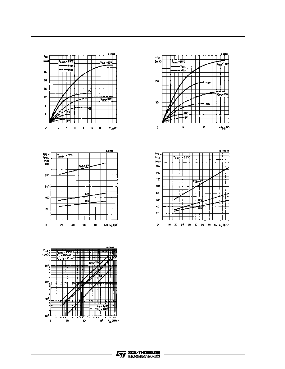
Output Low (sink) Current Characteristics.
Output High (source) Current Characteristics.
Typical Propagation Delay Time (clock to shift left
right) vs. Load Capacitance.
Typical Transition Time vs. Load Capacitance.
Typical Dynamic Power Dissipation vs. Clock Fre-
quency .
HCC/HCF40100B
7/13

Input Leakage Current.
Input Voltage.
TEST CIRCUITS
Quiescent Device Current.
HCC/HCF40100B
8/13

Plastic DIP16 (0.25) MECHANICAL DATA
DIM.
mm
inch
MIN.
TYP.
MAX.
MIN.
TYP.
MAX.
a1
0.51
0.020
B
0.77
1.65
0.030
0.065
b
0.5
0.020
b1
0.25
0.010
D
20
0.787
E
8.5
0.335
e
2.54
0.100
e3
17.78
0.700
F
7.1
0.280
I
5.1
0.201
L
3.3
0.130
Z
1.27
0.050
P001C
HCC/HCF40100B
9/13
Ceramic DIP16/1 MECHANICAL DATA
DIM.
mm
inch
MIN.
TYP.
MAX.
MIN.
TYP.
MAX.
A
20
0.787
B
7
0.276
D
3.3
0.130
E
0.38
0.015
e3
17.78
0.700
F
2.29
2.79
0.090
0.110
G
0.4
0.55
0.016
0.022
H
1.17
1.52
0.046
0.060
L
0.22
0.31
0.009
0.012
M
0.51
1.27
0.020
0.050
N
10.3
0.406
P
7.8
8.05
0.307
0.317
Q
5.08
0.200
P053D
HCC/HCF40100B
10/13

SO16 (Narrow) MECHANICAL DATA
DIM.
mm
inch
MIN.
TYP.
MAX.
MIN.
TYP.
MAX.
A
1.75
0.068
a1
0.1
0.2
0.004
0.007
a2
1.65
0.064
b
0.35
0.46
0.013
0.018
b1
0.19
0.25
0.007
0.010
C
0.5
0.019
c1
45
∞
(typ.)
D
9.8
10
0.385
0.393
E
5.8
6.2
0.228
0.244
e
1.27
0.050
e3
8.89
0.350
F
3.8
4.0
0.149
0.157
G
4.6
5.3
0.181
0.208
L
0.5
1.27
0.019
0.050
M
0.62
0.024
S
8
∞
(max.)
P013H
HCC/HCF40100B
11/13
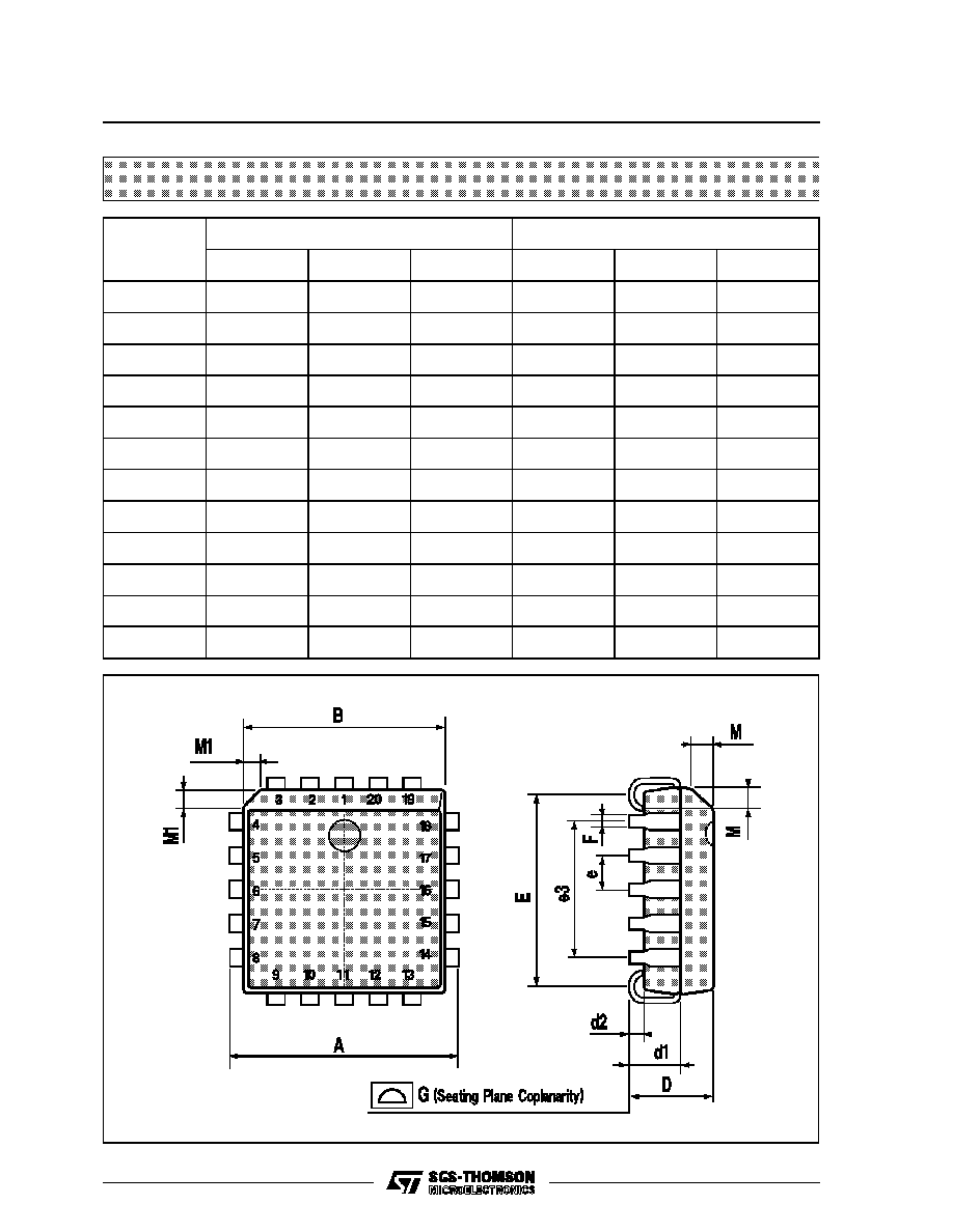
PLCC20 MECHANICAL DATA
DIM.
mm
inch
MIN.
TYP.
MAX.
MIN.
TYP.
MAX.
A
9.78
10.03
0.385
0.395
B
8.89
9.04
0.350
0.356
D
4.2
4.57
0.165
0.180
d1
2.54
0.100
d2
0.56
0.022
E
7.37
8.38
0.290
0.330
e
1.27
0.050
e3
5.08
0.200
F
0.38
0.015
G
0.101
0.004
M
1.27
0.050
M1
1.14
0.045
P027A
HCC/HCF40100B
12/13

Information furnished is believed to be accurate and reliable. However, SGS-THOMSON Microelectronics assumes no responsability for the
consequences of use of such information nor for any infringement of patents or other rights of third parties which may results from its use. No
license is granted by implication or otherwise under any patent or patent rights of SGS-THOMSON Microelectronics. Specifications mentioned
in this publication are subject to change without notice. This publication supersedes and replaces all information previously supplied.
SGS-THOMSON Microelectronics products are not authorized for use as critical components in life support devices or systems without express
written approval of SGS-THOMSON Microelectonics.
©
1994 SGS-THOMSON Microelectronics - All Rights Reserved
SGS-THOMSON Microelectronics GROUP OF COMPANIES
Australia - Brazil - France - Germany - Hong Kong - Italy - Japan - Korea - Malaysia - Malta - Morocco - The Netherlands -
Singapore - Spain - Sweden - Switzerland - Taiwan - Thailand - United Kingdom - U.S.A
HCC/HCF40100B
13/13