
HCC40106B
HCF40106B
HEX SCHMITT TRIGGERS
.
SCHMITT-TRIGGER ACTION WITH NO EX-
TERNAL COMPONENTS
.
HYSTERESIS VOLTAGE (TYP.) 0.9V AT V
DD
=
5V, 2.3V AT V
DD
= 10V AND 3.5V AT V
DD
= 15V
.
NOISE IMMUNITY GREATER THAN 50%
.
NO LIMIT ON INPUT RISE AND FALL TIME
.
LOW V
DD
TO V
SS
CURRENT DURING SLOW
INPUT RAMP
.
STANDARDIZED
SYMMETRICAL
OUTPUT
CHARACTERISTICS
.
QUIESCENT CURRENT SPECIFIED AT 20V
FOR HCC DEVICE
.
5V, 10V, AND 15V PARAMETRIC RATINGS
.
INPUT CURRENT OF 100nA AT 18V AND 25
∞
C
FOR HCC DEVICE
.
100% TESTED FOR QUIESCENT CURRENT
.
MEETS
ALL REQUIREMENTS OF JEDEC
TENTATIVE STANDARD N
∞
13A, "STANDARD
SPECIFICATIONS FOR DESCRIPTION OF "B"
SERIES CMOS DEVICES"
June 1989
EY
(Plastic Package)
F
(Ceramic Frit Seal Package)
C1
(Plastic Chip Carrier)
ORDER CODES :
HCC40106BF
HCF40106BM1
HCF40106BEY
HCF40106BC1
PIN CONNECTIONS
M1
(Micro Package)
DESCRIPTION
The HCC40106B (extended temperature range)
and HCF40106B (intermediate temperature range)
are monolithic integrated circuits, available in 14-
lead dual in-line plastic or ceramic package and
plastic micropackage.
The HCC/HCF40106B consists of six Schmitt-trig-
ger circuits. Each circuit functions as an inverter with
Schmitt-trigger action on the input. The trigger swit-
ches at different points for positive and negative-
going
signals.
The
difference
between
the
positive-going voltage (V
P
) and the negative-going
voltage (V
N
) is defined as hysteresis voltage (V
H
).
1/13
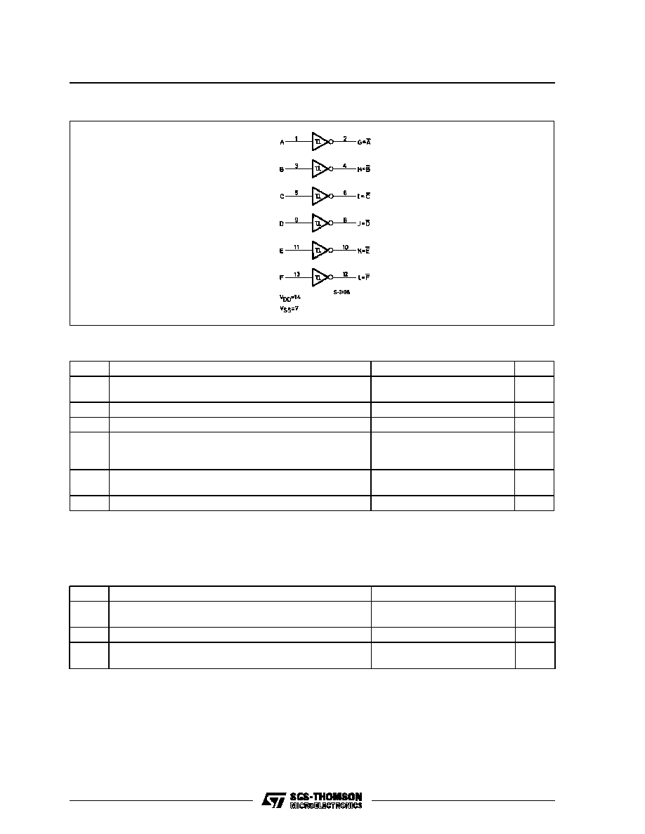
FUNCTIONAL DIAGRAM
ABSOLUTE MAXIMUM RATINGS
Symbol
Parameter
Value
Unit
V
DD
*
Supply Voltage : HC C Types
H C F Types
≠ 0.5 to + 20
≠ 0.5 to + 18
V
V
V
i
Input Voltage
≠ 0.5 to V
DD
+ 0.5
V
I
I
DC Input Current (any one input)
±
10
mA
P
t o t
Total Power Dissipation (per package)
Dissipation per Output Transistor
for T
o p
= Full Package-temperature Range
200
100
mW
mW
T
o p
Operating Temperature : HCC Types
H CF Types
≠ 55 to + 125
≠ 40 to + 85
∞
C
∞
C
T
s t g
Storage Temperature
≠ 65 to + 150
∞
C
RECOMMENDED OPERATING CONDITIONS
Symbol
Parameter
Value
Unit
V
DD
Supply Voltage : H CC Types
H C F Types
3 to 18
3 to 15
V
V
V
I
Input Voltage
0 to V
DD
V
T
o p
Operating Temperature : HCC Types
H CF Types
≠ 55 to + 125
≠ 40 to + 85
∞
C
∞
C
Stresses above those listed under "Absolute Maximum Ratings" may cause permanent damage to the device. This is a stress rating
only and functional operation of the device at these or any other conditions above those indicated in the operational sections of this
specification is not implied. Exposure to absolute maximum rating conditions for external periods may affect device reliability.
* All voltage values are referred to V
SS
pin voltage.
HCC/HCF40106B
2/13

LOGIC DIAGRAM
STATIC ELECTRICAL CHARACTERISTICS (over recommended operating conditions)
Test Conditions
Value
V
I
V
O
|I
O
|
V
D D
T
L o w
*
25
∞
C
T
Hi g h
*
Symbol
Parameter
(V)
(V)
(
µ
A)
(V)
Min. Max. Min. Typ. Max. Min. Max.
Unit
I
L
Quiescent
Current
HCC
Types
0/ 5
5
1
0.02
1
30
µ
A
0/10
10
2
0.02
2
60
0/15
15
4
0.02
4
120
0/20
20
20
0.04
20
600
HCF
Types
0/ 5
5
4
0.02
4
30
0/10
10
8
0.02
8
60
0/15
15
16
0.02
16
120
V
O H
Output High
Voltage
0/ 5
< 1
5
4.95
4.95
4.95
V
0/10
< 1
10
9.95
9.95
9.95
0/15
< 1
15
14.95
14.95
14.95
V
O L
Output Low
Voltage
5/10
< 1
5
0.05
0.05
0.05
V
10/0
< 1
10
0.05
0.05
0.05
15/0
< 1
15
0.05
0.05
0.05
V
P
Positive Trigger
Threshold
Voltage
5
2.2
3.6
2.2
2.9
3.6
2.2
3.6
V
10
4.6
7.1
4.6
5.9
7.1
4.6
7.1
15
6.8
10.8
6.8
8.8
10.8
6.8
10.8
V
N
Negative Trigger
Threshold
Voltage
5
0.9
2.8
0.9
1.9
2.8
0.9
2.8
V
10
2.5
5.2
2.5
3.9
5.2
2.5
5.2
15
4
7.4
4
5.8
7.4
4
7.4
V
H
Hysteresis
Voltage
5
0.3
1.6
0.3
0.9
1.6
0.3
1.6
V
10
1.2
3.4
1.2
2.3
3.4
1.2
3.4
15
1.6
5
1.6
3.5
5
1.6
* T
Low
= ≠ 55
∞
C for HCC device : ≠ 40
∞
C for HCF device.
* T
High
= + 125
∞
C for HCC device : + 85
∞
C for HCF device.
HCC/HCF40106B
3/13

DYNAMIC ELECTRICAL CHARACTERISTICS (T
amb
= 25
∞
C, C
L
= 50pF, R
L
= 200k
,
typical temperature coefficient for all V
D D
values is 0.3%/
∞
C, all input rise and fall time = 20ns)
Test Conditions
Val ue
Symbol
Parameter
V
D D
(V)
Min.
Typ.
Max.
Unit
t
PL H
,
t
PHL
Propagation Delay Time
5
140
280
ns
10
70
140
15
60
120
t
T HL
,
t
T L H
Transition Time
5
100
200
ns
10
50
100
15
40
80
STATIC ELECTRICAL CHARACTERISTICS (continued)
Test Conditions
Value
V
I
V
O
|I
O
|
V
D D
T
L o w
*
25
∞
C
T
Hi g h
*
Symbol
Parameter
(V)
(V)
(
µ
A)
(V)
Min. Max. Min. Typ. Max. Min. Max.
Unit
I
O H
Output
Drive
Current
HCC
Types
0/ 5
2.5
5
≠ 2
≠ 1.6 ≠ 3.2
≠ 1.15
mA
0/ 5
4.6
5
≠ 0.64
≠ 0.51 ≠ 1
≠ 0.36
0/10
9.5
10
≠ 1.6
≠ 1.3 ≠ 2.6
≠ 0.9
0/15
13.5
15
≠ 4.2
≠ 3.4 ≠ 6.8
≠ 2.4
HCF
Types
0/ 5
2.5
5
≠ 1.53
≠ 1.36 ≠ 3.2
≠ 1.1
0/ 5
4.6
5
≠ 0.52
≠ 0.44 ≠ 1
≠ 0.36
0/10
9.5
10
≠ 1.3
≠ 1.1 ≠ 2.6
≠ 0.9
0/15
13.5
15
≠ 3.6
≠ 3.0 ≠ 6.8
≠ 2.4
I
O L
Output Sink
Current
HCC
Types
0/ 5
0.4
5
0.64
0.51
1
0.36
mA
0/10
0.5
10
1.6
1.3
2.6
0.9
0/15
1.6
15
4.2
3.4
6.8
2.4
HCF
Types
0/ 5
0.4
5
0.52
0.44
1
0.36
0/10
0.5
10
1.3
1.1
2.6
0.9
0/15
1.5
15
3.6
3.0
6.8
2.9
I
IH
, I
IL
**
Input
Leakage
Current
HCC
Types
0/18
Any Input
18
±
0.1
±
10
≠ 5
±
0.1
±
1
µ
A
HCF
Types
0/15
15
±
0.3
±
10
≠ 5
±
0.3
±
1
C
I
Input Capacitance
Any Input
5
7.5
p
* T
Low
= ≠ 55
∞
C for HCC device : ≠ 40
∞
C for HCF device.
* T
High
= + 125
∞
C for HCC device : + 85
∞
C for HCF device.
HCC/HCF40106B
4/13

(a) Definition of V
P
, V
N
and V
H
.
(b) Transfer Characteristic of 1 of 6 gates.
(c) Test Setup.
Input and Output Characteristics.
Typical Current Voltage Transfer Characteristics, and Test Circuit.
HYSTERESIS DEFINITION, CHARACTERISTICS AND TEST SETUP
HCC/HCF40106B
5/13