
HCC/HCF4015B
INPUT/PARALLEL OUTPUT
DUAL 4-STAGE STATIC SHIFT REGISTER WITH SERIAL
.
MEDIUM SPEED OPERATION : 12MHz (typ.)
CLOCK RATE AT V
DD
- V
SS
= 10V
.
FULLY STATIC OPERATION
.
8 MASTER-SLAVE FLIP-FLOPS PLUS INPUT
AND OUTPUT BUFFERING
.
HIGH NOISE IMMUNITY
.
QUIESCENT CURRENT SPECIFIED TO 20V
FOR HCC DEVICE
.
INPUT CURRENT OF 100nA AT 18V AND 25
∞
C
FOR HCC DEVICE
.
100% TESTED FOR QUIESCENT CURRENT
.
5V, 10V, AND 15V PARAMETRIC RATINGS
.
MEETS ALL REQUIREMENTS OF JEDEC TEN-
TATIVE STANDARD N
O
. 13A, "STANDARD
SPECIFICATIONS FOR DESCRIPTION OF "B"
SERIES CMOS DEVICES"
June 1989
EY
(Plastic Package)
F
(Ceramic Frit Seal Package)
C1
(Plastic Chip Carrier)
ORDER CODES :
HCC4015BF
HCF4015BM1
HCF4015BEY
HCF4015BC1
PIN CONNECTIONS
M1
(Micro Package)
DESCRIPTION
The HCC4015B (extended temperature range) and
HCF4015B (intermediate temperature range) are
monolithic integrated circuits, available in 16-lead
dual in-line plastic or ceramic package and plastic
micropackage.
The HCC/HCF4015B consists of two identical, inde-
pendent, 4-stage serial-input/parallel-output registers.
Each register has independent CLOCK and RESET
inputs as well as a single serial DATA input. "Q" out-
puts are available from each of the four stages on both
registers. All register stages are D-type, master-slave
flip-flops. The logic level present at the DATA input is
transferred into the first register stage and shifted over
one stage at each positive-going clock transition. Re-
setting of all stages is accomplished by a high level on
the reset line. Register expansion to 8 stages using
one HCC/HCF4015B package, or to more than 8
stages using additional HCC/HCF4015B's is possible.
1/12

FUNCTIONAL DIAGRAM
ABSOLUTE MAXIMUM RATINGS
Symbol
Parameter
Value
Unit
V
DD
*
Supply Voltage : HC C Types
H CF Types
≠ 0.5 to + 20
≠ 0.5 to + 18
V
V
V
i
Input Voltage
≠ 0.5 to V
DD
+ 0.5
V
I
I
DC Input Current (any one input)
±
10
mA
P
t o t
Total Power Dissipation (per package)
Dissipation per Output Transistor
for T
o p
= Full Package-temperature Range
200
100
mW
mW
T
o p
Operating Temperature : HCC Types
H CF Types
≠ 55 to + 125
≠ 40 to + 85
∞
C
∞
C
T
s t g
Storasge Temperature
≠ 65 to + 150
∞
C
RECOMMENDED OPERATING CONDITIONS
Symbol
Parameter
Value
Unit
V
DD
Supply Voltage : HCC Types
HC F Types
3 to 18
3 to 15
V
V
V
I
Input Voltage
0 to V
DD
V
T
o p
Operating Temperature : HCC Types
H CF Types
≠ 55 to + 125
≠ 40 to + 85
∞
C
∞
C
Stresses above those listed under "Absolute Maximum Ratings "may cause permanent damage to the device. This is a stress
rating only and functional operation of the device at these or any other conditions above those indicated in the operational sec-
tions of this specifi cation is not implied. Exposure to absolute maximum rating conditions for external periods may affect device
reliability.
* All voltage values are referred to V
SS
pin voltage.
HCC/HCF4015B
2/12

LOGIC DIAGRAMS AND TRUTH TABLE
CL
D
R
Q
1
Q
n
≠
/
≠
0
0
0
Q
n ≠ 1
≠
/
≠
1
0
1
Q
n ≠ 1
≠\
≠
X
0
Q
1
Q
n
≠
(no. change)
X
X
1
0
0
HCC/HCF4015B
3/12

STATIC ELECTRICAL CHARACTERISTICS (over recommended operating conditions)
Test Conditions
Val ue
V
I
V
O
| I
O
|
V
DD
T
Lo w
*
25
∞
C
T
High
*
Symbol
Parameter
(V)
(V)
(
µ
A)
(V)
Min.
Max.
Min.
Typ.
Max.
Min.
Max.
Unit
I
L
Quiescent
Current
HCC
Types
0/ 5
5
5
0.04
5
150
µ
A
0/10
10
10
0.04
10
300
0/15
15
20
0.04
20
600
0/20
20
100
0.08
100
3000
HCF
Types
0/ 5
5
20
0.04
20
150
0/10
10
40
0.04
40
300
0/15
15
80
0.04
80
600
V
OH
Output High
Voltage
0/ 5
< 1
5
4.95
4.95
4.95
V
0/10
< 1
10
9.95
9.95
9.95
0/15
< 1
15
14.95
14.95
14.95
V
OL
Output Low
Voltage
5/0
< 1
5
0.05
0.05
0.05
V
10/0
< 1
10
0.05
0.05
0.05
15/0
< 1
15
0.05
0.05
0.05
V
IH
Input High
Voltage
0.5/4.5
< 1
5
3.5
3.5
3.5
V
1/9
< 1
10
7
7
7
1.5/13.5
< 1
15
11
11
11
V
IL
Input Low
Voltage
4.5/0.5
< 1
5
1.5
1.5
1.5
V
9/1
< 1
10
3
3
3
13.5/1.5
< 1
15
4
4
4
I
OH
Output
Drive
Current
HCC
Types
0/ 5
2.5
5
≠ 2
≠ 1.6 ≠ 3.2
≠ 1.15
mA
0/ 5
4.6
5
≠ 0.64
≠ 0. 51
≠ 1
≠ 0.36
0/10
9.5
10
≠ 1. 6
≠ 1.3 ≠ 2.6
≠ 0.9
0/15
13.5
15
≠ 4. 2
≠ 3.4 ≠ 6.8
≠ 2.4
HCF
Types
0/ 5
2.5
5
≠ 1.53
≠ 1. 36
≠ 3.2
≠ 1.1
0/ 5
4.6
5
≠
0.52
≠
0.44
≠ 1
≠
0.36
0/10
9.5
10
≠ 1. 3
≠ 1.1 ≠ 2.6
≠ 0.9
0/15
13.5
15
≠ 3. 6
≠ 3.0 ≠ 6.8
≠ 2.4
I
OL
Output
Sink
Current
HCC
Types
0/ 5
0.4
5
0.64
0.51
1
0.36
mA
0/10
0.5
10
1.6
1.3
2.6
0.9
0/15
1.5
15
4.2
3.4
6.8
2.4
HCF
Types
0/ 5
0.4
5
0.52
0.44
1
0.36
0/10
0.5
10
1.3
1.1
2.6
0.9
0/15
1.5
15
3.6
3.0
6.8
2.4
I
IH
, I
IL
Input
Leakage
Current
HCC
Types
0/18
Any Input
18
±
0. 1
±
10
≠5
±
0.1
±
1
µ
A
HCF
Types
0/15
15
±
0. 3
±
10
≠5
±
0.3
±
1
C
I
Input Capacitance
Any Input
5
7.5
pF
* T
Lo w
= ≠ 55
∞
C for HCC device : ≠ 40
∞
C for HCF device.
* T
High
= + 125
∞
C for HCC device : + 85
∞
C for HCF device.
The Noise Margin for both "1" and "0" level is : 1V min. with V
DD
= 5V, 2V min. with V
DD
= 10V, 2.5 V min. with V
DD
= 15V.
HCC/HCF4015B
4/12

DYNAMIC ELECTRICAL CHARACTERISTICS (T
amb
= 25
∞
C, C
L
= 50 pF, R
L
= 200 k
,
typical temperature coefficient for all V
DD
values is 0.3 %/
∞
C, all input rise and fall times = 20 ns)
Val ue
Symbol
Parameter
Test Conditions
V
D D
(V)
Min.
Typ.
Max.
Unit
CLOCKED OPERATI ON
t
P L H
, t
P HL
Propagation Delay Time
(carry out or decoded out lines)
5
160
320
ns
10
80
160
15
60
120
t
THL
, t
T L H
Transition Time
(carry out or decoded out lines)
5
100
200
ns
10
50
100
15
40
80
f
CL
Maximum Clock Input Frequency
5
3
6
MHz
10
6
12
15
8.5
17
t
W
Clock Pulse Width
5
180
90
ns
10
80
40
15
50
25
t
r
, t
f
*
Clock Input Rise or Fall Time
5
15
µ
s
10
15
15
15
t
se t u p
Data Setup Time
5
70
35
ns
10
40
20
15
30
15
RESET OPERATI ON
t
P L H
, t
P HL
Propagation Delay Time
5
200
400
ns
10
100
200
15
80
160
t
W
Reset Pulse Width
5
200
100
ns
10
80
40
15
60
30
* If more than unit is cascaded in the parallel clocked application, t
r
CL should be made less than or equal to the sum of the fixed propagation delay
at 15pF and the transition time of the carry output driving stage for the estimated capacitive load.
HCC/HCF4015B
5/12

Typical Output Low (sink) Current Characteristics.
Minimum Output Low (sink) Current Characteristics.
Typical Output High (source) Current Charac-
teristics.
Minimum Output High (source) Current Charac-
teristics.
Typical propagation Delay Time vs. Load Capacit-
ance..
Typical transition Time vs. Load Capacitance.
HCC/HCF4015B
6/12
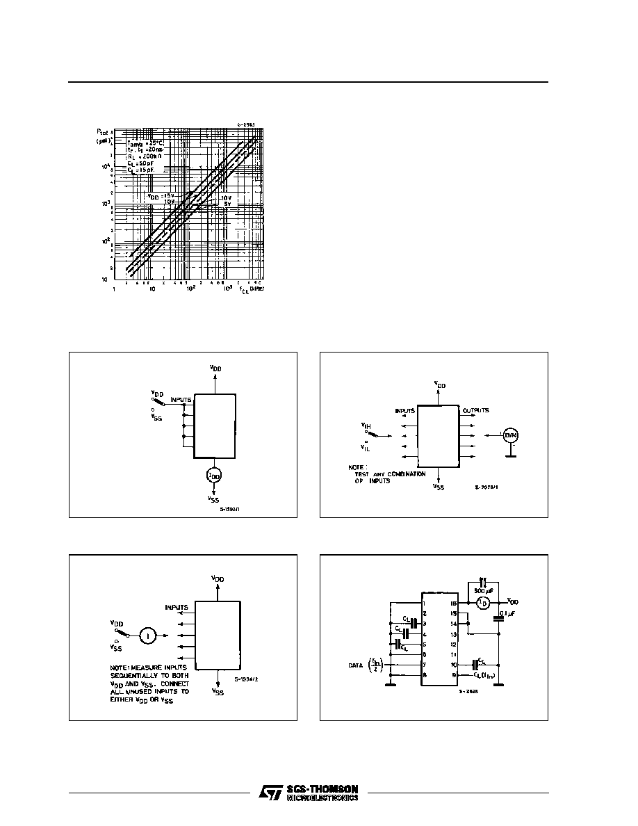
Typical Dynamic Power Dissipation vs. Frequency.
Input Voltage.
Input current.
TEST CIRCUITS
Quiescent Device Current.
Power Dissipation.
HCC/HCF4015B
7/12

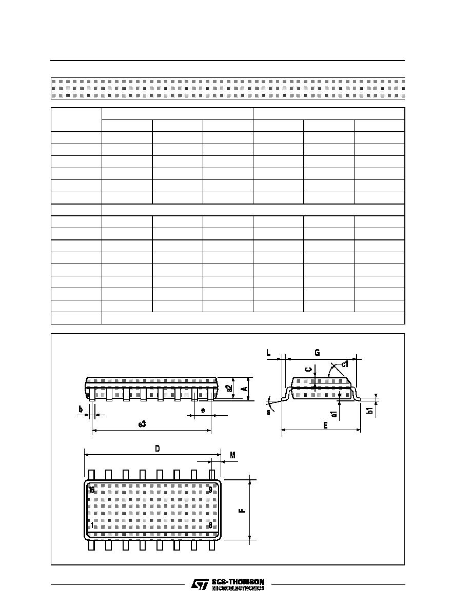
Plastic DIP16 (0.25) MECHANICAL DATA
DIM.
mm
inch
MIN.
TYP.
MAX.
MIN.
TYP.
MAX.
a1
0.51
0.020
B
0.77
1.65
0.030
0.065
b
0.5
0.020
b1
0.25
0.010
D
20
0.787
E
8.5
0.335
e
2.54
0.100
e3
17.78
0.700
F
7.1
0.280
I
5.1
0.201
L
3.3
0.130
Z
1.27
0.050
P001C
HCC/HCF4015B
8/12

Ceramic DIP16/1 MECHANICAL DATA
DIM.
mm
inch
MIN.
TYP.
MAX.
MIN.
TYP.
MAX.
A
20
0.787
B
7
0.276
D
3.3
0.130
E
0.38
0.015
e3
17.78
0.700
F
2.29
2.79
0.090
0.110
G
0.4
0.55
0.016
0.022
H
1.17
1.52
0.046
0.060
L
0.22
0.31
0.009
0.012
M
0.51
1.27
0.020
0.050
N
10.3
0.406
P
7.8
8.05
0.307
0.317
Q
5.08
0.200
P053D
HCC/HCF4015B
9/12
SO16 (Narrow) MECHANICAL DATA
DIM.
mm
inch
MIN.
TYP.
MAX.
MIN.
TYP.
MAX.
A
1.75
0.068
a1
0.1
0.2
0.004
0.007
a2
1.65
0.064
b
0.35
0.46
0.013
0.018
b1
0.19
0.25
0.007
0.010
C
0.5
0.019
c1
45
∞
(typ.)
D
9.8
10
0.385
0.393
E
5.8
6.2
0.228
0.244
e
1.27
0.050
e3
8.89
0.350
F
3.8
4.0
0.149
0.157
G
4.6
5.3
0.181
0.208
L
0.5
1.27
0.019
0.050
M
0.62
0.024
S
8
∞
(max.)
P013H
HCC/HCF4015B
10/12

PLCC20 MECHANICAL DATA
DIM.
mm
inch
MIN.
TYP.
MAX.
MIN.
TYP.
MAX.
A
9.78
10.03
0.385
0.395
B
8.89
9.04
0.350
0.356
D
4.2
4.57
0.165
0.180
d1
2.54
0.100
d2
0.56
0.022
E
7.37
8.38
0.290
0.330
e
1.27
0.050
e3
5.08
0.200
F
0.38
0.015
G
0.101
0.004
M
1.27
0.050
M1
1.14
0.045
P027A
HCC/HCF4015B
11/12

Information furnished is believed to be accurate and reliable. However, SGS-THOMSON Microelectronics assumes no responsability for the
consequences of use of such information nor for any infringement of patents or other rights of third parties which may results from its use. No
license is granted by implication or otherwise under any patent or patent rights of SGS-THOMSON Microelectronics. Specifications mentioned
in this publication are subject to change without notice. This publication supersedes and replaces all information previously supplied.
SGS-THOMSON Microelectronics products are not authorized for use as critical components in life support devices or systems without express
written approval of SGS-THOMSON Microelectonics.
©
1994 SGS-THOMSON Microelectronics - All Rights Reserved
SGS-THOMSON Microelectronics GROUP OF COMPANIES
Australia - Brazil - France - Germany - Hong Kong - Italy - Japan - Korea - Malaysia - Malta - Morocco - The Netherlands -
Singapore - Spain - Sweden - Switzerland - Taiwan - Thailand - United Kingdom - U.S.A
HCC/HCF4015B
12/12