 | –≠–ª–µ–∫—Ç—Ä–æ–Ω–Ω—ã–π –∫–æ–º–ø–æ–Ω–µ–Ω—Ç: HCF40181 | –°–∫–∞—á–∞—Ç—å:  PDF PDF  ZIP ZIP |

HCC/HCF40181B
June 1989
4-BIT ARITHMETIC LOGIC UNIT
.
FULL LOOK-AHEAD CARRY FOR SPEED
OPERATIONS ON LONG WORDS
.
GENERATES 16 LOGIC FUNCTIONS OF TWO
BOOLEAN VARIABLES
.
GENERATES 16 ARITHMETIC FUNCTIONS
OF TWO 4-BIT BINARY WORDS
.
A = B COMPARATOR OUTPUT AVAILABLE
.
RIPPLE-CARRY INPUT AND OUTPUT AVAIL-
ABLE
.
TYPICAL ADDITION TIME 200ns @ V
DD
= 10V
.
STANDARDIZED
SYMMETRICAL
OUTPUT
CHARACTERISTICS
.
QUIESCENT CURRENT AT 20V FOR HCC DE-
VICE
.
5V, 10V, AND 15V PARAMETRIC RATINGS
.
INPUT CURRENT OF 100nA AT 18V AND 25
∞
C
FOR HCC DEVICE
.
100% TESTED FOR QUIESCENT CURRENT
.
MEETS ALL REQUIREMENTS OF JEDEC TEN-
TATIVE STANDARD N
∞
13A, "STANDARD SPE-
CIFICATIONS FOR DESCRIPTION OF "B"
SERIES CMOS DEVICES"
DESCRIPTION
The HCC40181B (extended temperature range)
and HCF40181B (intermediate temperature range)
are monolithic integrated circuits, available in 24-
lead dual in-line plastic or ceramic package and
plastic micro package. The HCC/HCF40181B is a
low-power four-bit parallel arithmetic logic unit
(ALU) capable of providing 16 binary arithmetic
operations on two four-bit words and 16 logical func-
tions of two Boolean variables. The mode control
input M selects logical (M = High) or arithmetic (M =
Low) operation. The four select inputs (S0, S1, S2,
and S3) select the desired logical or arithmetic func-
tions, which include AND, OR, NAND, NOR, and ex-
clusive-OR and-NOR in the logical mode, and
addition, subtraction, decrement, left-shift and
straight transfer in the arithmetic mode, according to
the truth table. The HCC/HCF40181B operation
may be interpreted with either active-low or active-
high data at the A and B word inputs and the function
outputs F, by using the appropriate truth table. The
HCC/HCF40181B contains logic for full look-ahead
carry operation for fast carry generation using the
carry-generate and carry-propagate outputs G and
EY
(Plastic Package)
F
(Ceramic Frit Seal Package)
ORDER CODES :
HCC40181BF
HCF40181BEY
HCF40181BM1
PIN CONNECTIONS
M1
(Micro Package)
1/12

P for the four bits of the HCC/HCF40181B. Use of
the HCC/HCF40182B look-ahead carry generator
in conjunction with multiple HCC/HCF40181B's per-
mits high-speed arithmetic operations on long
words. A ripple carry output C
n + 4
is available for use
in systems where speed is not of primary import-
ance. Also included in the HCC/HCF40181B is a
comparator output A = B, which assumes a high
level whenever the two four-bit input words A and B
are equal and the device is in the subtract mode. In
addition, relative magnitude information may be
derived from the carry-in input C
n
and ripple carry-
out output C
n + 4
by placing the unit in the subtract
mode and externally decoding using the information
in table II. The HCC/HCF40181B is similar to indus-
try types MC 14581 and 74181.
FUNCTIONAL DIAGRAM
Active-low Data.
Active-high Data.
ABSOLUTE MAXIMUM RATINGS
Symbol
Parameter
Value
Unit
V
DD
*
Supply Voltage : HC C Types
H C F Types
≠ 0.5 to + 20
≠ 0.5 to + 18
V
V
V
i
Input Voltage
≠ 0.5 to V
DD
+ 0.5
V
I
I
DC Input Current (any one input)
±
10
mA
P
t o t
Total Power Dissipation (per package)
Dissipation per Output Transistor
for T
o p
= Full Package-temperature Range
200
100
mW
mW
T
o p
Operating Temperature : HCC Types
H CF Types
≠ 55 to + 125
≠ 40 to + 85
∞
C
∞
C
T
s t g
Storage Temperature
≠ 65 to + 150
∞
C
Stresses above those listed under "Absolute Maximum Ratings" may cause permanent damage to the device. This is a stress
rating only and functional operation of the device at these or any other conditions above those indicated in the operational sections
of this specification is not implied. Exposure to absolute maximum rating conditions for external periods may affect device reliability.
* All voltages are with respect to V
SS
(GND).
HCC/HCF40181B
2/12
RECOMMENDED OPERATING CONDITIONS
Symbol
Parameter
Value
Unit
V
DD
Supply Voltage : H CC Types
H C F Types
3 to 18
3 to 15
V
V
V
I
Input Voltage
0 to V
DD
V
T
o p
Operating Temperature : HCC Types
H CF Types
≠ 55 to + 125
≠ 40 to + 85
∞
C
∞
C
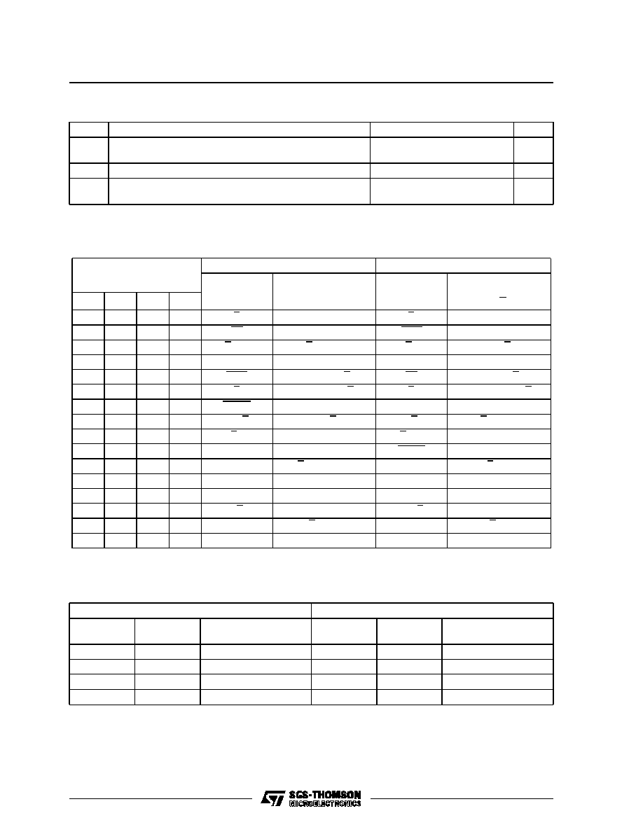
TRUTH TABLES
Table 1.
Inputs/Outputs Active Low
Inputs/Outputs Active High
Function
Select
S 3
S 2
S 1
S 0
Logic
Function
(M = H)
Arithmetic*
Function
(M = L, C
n
= L)
Logic
Function
(M = H)
Arithmetic*
Function
(M = L, C
n
= H)
0
0
0
0
A
A minus 1
A
A
0
0
0
1
AB
AB minus 1
A + B
A + B
0
0
1
0
A + B
AB minus 1
AB
A + B
0
0
1
1
Logic 1
minus 1
Logic 0
minus 1
0
1
0
0
A + B
A plus (A + B)
AB
A plus AB
0
1
0
1
B
AB plus (A + B)
B
(A + B) plus AB
0
1
1
0
A
B
A minus B minus 1
A
B
A minus B minus 1
0
1
1
1
A + B
A + B
AB
AB minus 1
1
0
0
0
AB
A plus (A + B)
A + B
A plus AB
1
0
0
1
A
B
A plus B
A
B
A plus B
1
0
1
0
B
AB plus (A + B)
B
(A + B) plus AB
1
0
1
1
A + B
A + B
AB
AB minus 1
1
1
0
0
Logic 0
A plus A
Logic 1
A plus A
1
1
0
1
AB
AB plus A
A + B
(A + B) plus A
1
1
1
0
AB
AB plus A
A + B
(A + B) plus A
1
1
1
1
A
A
A
A minus 1
* Expressed as two's complement. For arithmetic function with C
n
in the opposite state, the resulting function is as show plus 1.
1 = HIGH LEVEL.
0 = LOW LEVEL.
Table 2 : Magnitude Comparison.
Active-high D ata
Active-low Data
Input
C
n
Output
C
n + 4
Magni tude
Input
C
n
Output
C
n + 4
Magni tude
1
1
A
B
0
0
A
B
0
1
A < B
1
0
A < B
1
0
A > B
0
1
A > B
0
0
A
B
1
1
A
B
1 = HIGH LEVEL
0 = LOW LEVEL
HCC/HCF40181B
3/12

LOGIC DIAGRAM Active-low Data
HCC/HCF40181B
4/12
STATIC ELECTRICAL CHARACTERISTICS (over recommended operating conditions)
Test Conditions
Value
V
I
V
O
|I
O
|
V
D D
T
L o w
*
25
∞
C
T
Hi g h
*
Symbol
Parameter
(V)
(V)
(
µ
A)
(V)
Min. Max. Min. Typ. Max. Min. Max.
Unit
I
L
Quiescent
Current
HCC
Types
0/ 5
5
5
0.04
5
150
µ
A
0/10
10
10
0.04
10
300
0/15
15
20
0.04
20
600
0/20
20
100
0.08
100
3000
HCF
Types
0/ 5
5
20
0.04
20
150
0/10
10
40
0.04
40
300
0/15
15
80
0.04
80
600
V
O H
Output High
Voltage
0/ 5
< 1
5
4.95
4.95
4.95
V
0/10
< 1
10
9.95
9.95
9.95
0/15
< 1
15
14.95
14.95
14.95
V
O L
Output Low
Voltage
5/0
< 1
5
0.05
0.05
0.05
V
10/0
< 1
10
0.05
0.05
0.05
15/0
< 1
15
0.05
0.05
0.05
V
IH
Input High
Voltage
0.5/4.5
< 1
5
3.5
3.5
3.5
V
1/9
< 1
10
7
7
7
1.5/13.5
< 1
15
11
11
11
V
IL
Input Low
Voltage
4.5/0.5
< 1
5
1.5
1.5
1.5
V
9/1
< 1
10
3
3
3
13.5/1.5
< 1
15
4
4
4
I
O H
Output
Drive
Current
HCC
Types
0/ 5
2.5
5
≠ 2
≠ 1.6 ≠ 3.2
≠ 1.15
mA
0/ 5
4.6
5
≠ 0.64
≠ 0.51 ≠ 1
≠ 0.36
0/10
9.5
10
≠ 1.6
≠ 1.3 ≠ 2.6
≠ 0.9
0/15
13.5
15
≠ 4.2
≠ 3.4 ≠ 6.8
≠ 2.4
HCF
Types
0/ 5
2.5
5
≠ 1.53
≠ 1.36 ≠ 3.2
≠ 1.1
0/ 5
4.6
5
≠ 0.52
≠ 0.44 ≠ 1
≠ 0.36
0/10
9.5
10
≠ 1.3
≠ 1.1 ≠ 2.6
≠ 0.9
0/15
13.5
15
≠ 3.6
≠ 3.0 ≠ 6.8
≠ 2.4
I
O L
Output
Sink
Current
HCC
Types
0/ 5
0.4
5
0.64
0.51
1
0.36
mA
0/10
0.5
10
1.6
1.3
2.6
0.9
0/15
1.5
15
4.2
3.4
6.8
2.4
HCF
Types
0/ 5
0.4
5
0.52
0.44
1
0.36
0/10
0.5
10
1.3
1.1
2.6
0.9
0/15
1.5
15
3.6
3.0
6.8
2.4
I
IH
, I
IL
Input
Leakage
Current
HCC
Types
0/18
Any Input
18
±
0.1
±
10
≠ 5
±
0.1
±
1
µ
A
HCF
Types
0/15
15
±
0.3
±
10
≠ 5
±
0.3
±
1
C
I
Input Capacitance
Any Input
5
7.5
pF
* T
Lo w
= ≠ 55
∞
C for HCC device : ≠ 40
∞
C for HCF device.
* T
High
= + 125
∞
C for HCC device : + 85
∞
C for HCF device.
The Noise Margin for both "1" and " 0" level is : 1V min. with V
DD
= 5V, 2V min. with V
DD
= 10V, 2.5V min. with V
DD
= 15V.
HCC/HCF40181B
5/12

Table 3 : AC Test Setup Reference (active-low data).
AC Paths
D C Data Inputs
Test
Delay Times
Inputs
Outputs
to V
S S
to V
D D
Mo de*
SUM
IN
to SUM
O UT
BO
Any F
B1, B2, B3,
M, C
n
All A's
ADD
SUM
IN
to P
AO
P
A1, A2, A3,
M, C
n
All B's
ADD
SUM
IN
to G
BO
G
All A's
M, C
n
B1, B2, B3
ADD
SUM
IN
to C
n + 4
BO
C
n + 4
All A's,
M, C
n
B1, B2, B3
ADD
C
n
to SUM
OUT
C
n
Any F
All A's,
M
All B's
ADD
C
n
to C
n + 4
C
n
C
n + 4
All A's,
M
All B's
ADD
SUM
IN
to A = B
BO
A = B
All A's
B1, B2, B3,
M
C
n
SUBTRACT
SUM
IN
to SUM
O UT
(logic mode)
All B's
Any F
All A's,
C
n
M
EXCLUSIVE
OR
* ADD Mode : S0, S3 = V
DD
; S1, S2 = V
SS
. SUBTRACT Mode : S0, S3 = V
SS
; S1, S2 = V
DD
.
DYNAMIC ELECTRICAL CHARACTERISTICS (T
amb
= 25
∞
C, C
L
= 50pF, R
L
= 200k
,
typical temperature coefficient for all V
DD
values is 0.3%/
∞
C, all input rise and fall time = 20ns)
Test Conditions
Val ue
Symbol
Parameter
V
D D
(V)
Min.
Typ.
Max.
Unit
t
PL H
,
t
PHL
Propagation Delay Time
A or B to F (logic mode)
A or B to G or P
5
400
800
ns
10
160
320
15
120
240
A or B to F,
C
n + 4
, or A = B
5
300
1000
ns
10
200
400
15
140
280
C
n
to F
5
320
640
ns
10
135
270
15
100
200
C
n
to C
n + 4
5
200
400
ns
10
100
200
15
70
140
t
T L H
,
t
THL
Transition Time
5
100
200
ns
10
50
100
15
40
80
HCC/HCF40181B
6/12

Output Low (sink) Current Characteristics.
Output High (source) Current Characteristics.
Typical Propagation Delay Time vs. Load Capacit-
ance
(for A or B to F, logic mode).
Typical Dynamic Power Dissipation vs. Input Fre-
quen
HCC/HCF40181B
7/12

TEST CIRCUITS
Quiescent Device Current.
Input Voltage.
Input Leakage Current.
Dynamic Power Dissipation.
HCC/HCF40181B
8/12
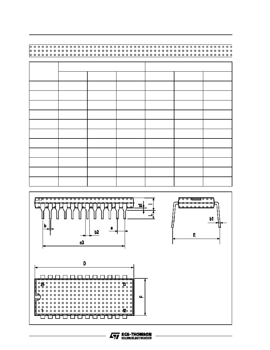
Plastic DIP24 (0.25) MECHANICAL DATA
DIM.
mm
inch
MIN.
TYP.
MAX.
MIN.
TYP.
MAX.
a1
0.63
0.025
b
0.45
0.018
b1
0.23
0.31
0.009
0.012
b2
1.27
0.050
D
32.2
1.268
E
15.2
16.68
0.598
0.657
e
2.54
0.100
e3
27.94
1.100
F
14.1
0.555
I
4.445
0.175
L
3.3
0.130
P043A
HCC/HCF40181B
9/12

Ceramic DIP24 MECHANICAL DATA
DIM.
mm
inch
MIN.
TYP.
MAX.
MIN.
TYP.
MAX.
A
32.3
1.272
B
13.05
13.36
0.514
0.526
C
3.9
5.08
0.154
0.200
D
3
0.118
E
0.5
1.78
0.020
0.070
e3
27.94
1.100
F
2.29
2.79
0.090
0.110
G
0.4
0.55
0.016
0.022
I
1.17
1.52
0.046
0.060
L
0.22
0.31
0.009
0.012
M
1.52
2.49
0.060
0.098
N1
4
∞
(min.), 15
∞
(max.)
P
15.4
15.8
0.606
0.622
Q
5.71
0.225
P058C
HCC/HCF40181B
10/12
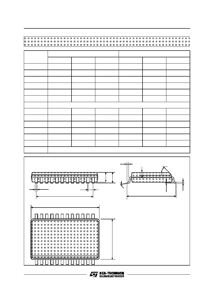
SO24 MECHANICAL DATA
DIM.
mm
inch
MIN.
TYP.
MAX.
MIN.
TYP.
MAX.
A
2.65
0.104
a1
0.10
0.20
0.004
0.007
a2
2.45
0.096
b
0.35
0.49
0.013
0.019
b1
0.23
0.32
0.009
0.012
C
0.50
0.020
c1
45
∞
(typ.)
D
15.20
15.60
0.598
0.614
E
10.00
10.65
0.393
0.420
e
1.27
0.05
e3
13.97
0.55
F
7.40
7.60
0.291
0.299
L
0.50
1.27
0.19
0.050
S
8
∞
(max.)
F
C
L
E
a1
b1
A
e
D
e3
b
24
13
1
12
c1
s
a2
HCC/HCF40181B
11/12
Information furnished is believed to be accurate and reliable. However, SGS-THOMSON Microelectronics assumes no responsability for the
consequences of use of such information nor for any infringement of patents or other rights of third parties which may results from its use. No
license is granted by implication or otherwise under any patent or patent rights of SGS-THOMSON Microelectronics. Specifications mentioned
in this publication are subject to change without notice. This publication supersedes and replaces all information previously supplied.
SGS-THOMSON Microelectronics products are not authorized for use as critical components in life support devices or systems without express
written approval of SGS-THOMSON Microelectonics.
©
1994 SGS-THOMSON Microelectronics - All Rights Reserved
SGS-THOMSON Microelectronics GROUP OF COMPANIES
Australia - Brazil - France - Germany - Hong Kong - Italy - Japan - Korea - Malaysia - Malta - Morocco - The Netherlands -
Singapore - Spain - Sweden - Switzerland - Taiwan - Thailand - United Kingdom - U.S.A
HCC/HCF40181B
12/12