
HCC/HCF40182B
June 1989
LOOK-AHEAD CARRY GENERATOR
.
GENERATES HIGH-SPEED CARRY ACROSS
FOUR ADDERS OF ADDER GROUPS
.
HIGH-SPEED OPERATIONAL : t
PHL
= t
PLH
=
100ns (typ.) @ V
DD
= 10V
.
CASCADABLE FOR FAST CARRIES OVER N
BITS
.
DESIGNED FOR USE WITH HCC/HCF40181B
ALU
.
STANDARDIZED, SYMMETRICAL OUTPUT
CHARACTERISTICS
.
QUIESCENT CURRENT SPECIFIED AT 20V
FOR HCC DEVICE
.
5V, 10V, AND 15V PARAMETRIC RATINGS
.
INPUT CURRENT OF 100nA AT 18V AND 25
∞
C
FOR HCC DEVICE
.
100% TESTED FOR QUIESCENT CURRENT
.
MEETS ALL REQUIREMENTS OF JEDEC TEN-
TATIVE STANDARD N
∞
13A, "STANDARD SPE-
CIFICATIONS FOR DESCRIPTION OF "B"
SERIES CMOS DEVICES"
DESCRIPTION
The HCC40182B (extended temperature range)
and HCF40182B (intermediate temperature range)
are monolithic integrated circuits, available in 16-
lead dual in-line plastic or ceramic package and
plastic micro package. The HCC/HCF40182B is a
high-speed look-ahead carry generator capable of
anticipating a carry across four binary adders or
groups of adders. The HCC/HCF40182B is cascad-
able to perform full look-ahead across n-bit adders.
Carry, propagate-carry, and generate-carry func-
tions are provided as enumerated in the terminal
designation below. The HCC/HCF40182B, when
used in conjunction with the HCC/HCF40181B
arithmetic logic unit (ALU), provides full high-speed
look-ahead carry capability for up to n-bit words.
Each HCC/HCF40182B generates the look-ahead
(anticipated carry) across a group of four ALU's. In
addition, other HCC/HCF40182B's may be em-
played to anticipate the carry across sections of four
look-ahead blocks up to n-bits. Carry inputs and out-
puts of the HCC/HCF40181B are active-high logic,
and carry-generate (G) and carry-propagate (P) out-
puts are active low. Therefore the inputs and outputs
of the HCC/HCF40182B are compatible. The
HCC/HCF40182B
is similar to industry type
MC14582.
EY
(Plastic Package)
F
(Ceramic Frit Seal Package)
C1
(Plastic Chip Carrier)
ORDER CODES :
HCC40182BFHCF4018
2BM1
PIN CONNECTIONS
M1
(Micro Package)
1/12

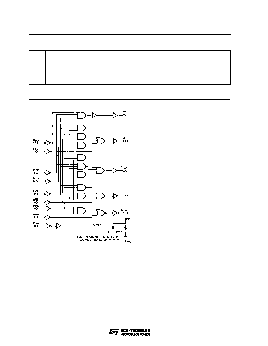
FUNCTIONAL DIAGRAM
TERMINAL DESIGNATIONS TABLE
Pin Name
Pin
Function
G0, G1, G2, G3
3, 1, 14, 5
Active-low Carry-generate Inputs
P0, P1, P2, P3
4, 2, 15, 6
Active-low Carry-propagate Inputs
C
n
13
Active-high Carry Input
C
n + X
, C
n + Y
,
C
n + Z
12, 11, 9
Active-high Carry Outputs
G
10
Active-low Group Carry-generate Output
P
7
Active-low Group Carry-propagate Output
ABSOLUTE MAXIMUM RATINGS
Symbol
Parameter
Value
Unit
V
DD
*
Supply Voltage : HC C Types
H C F Types
≠ 0.5 to + 20
≠ 0.5 to + 18
V
V
V
i
Input Voltage
≠ 0.5 to V
DD
+ 0.5
V
I
I
DC Input Current (any one input)
±
10
mA
P
t o t
Total Power Dissipation (per package)
Dissipation per Output Transistor
for T
o p
= Full Package-temperature Range
200
100
mW
mW
T
o p
Operating Temperature : HCC Types
H CF Types
≠ 55 to + 125
≠ 40 to + 85
∞
C
∞
C
T
s t g
Storage Temperature
≠ 65 to + 150
∞
C
Stresses above those listed under "Absolute Maximum Ratings" may cause permanent damage to the device. This is a stress
rating only and functional operation of the device at these or any other conditions above those indicated in the operational sections
of this specification is not implied. Exposure to absolute maximum rating conditions for external periods may affect device reliability.
* All voltages are with respect to V
SS
(GND).
HCC/HCF40182B
2/12
RECOMMENDED OPERATING CONDITIONS
Symbol
Parameter
Value
Unit
V
DD
Supply Voltage : H CC Types
H C F Types
3 to 18
3 to 15
V
V
V
I
Input Voltage
0 to V
DD
V
T
o p
Operating Temperature : HCC Types
H CF Types
≠ 55 to + 125
≠ 40 to + 85
∞
C
∞
C
LOGIC DIAGRAM
Logic Equations :
C
n + X
= G0 + P0
∑
Cn
C
n + Y
= G1 + P1
∑
G0 + P1
∑
P0
∑
C
n
HCC/HCF40182B
3/12
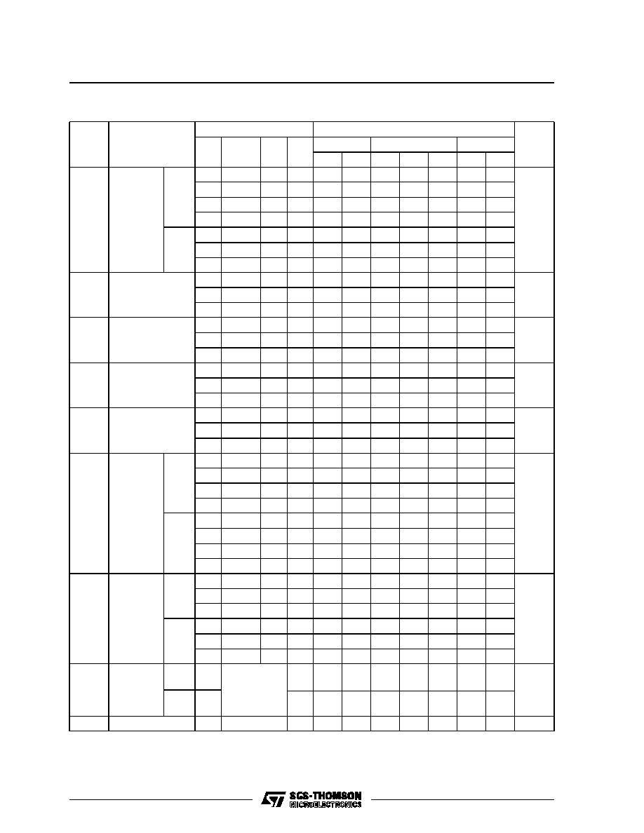
STATIC ELECTRICAL CHARACTERISTICS (over recommended operating conditions)
Test Conditions
Value
V
I
V
O
|I
O
|
V
DD
T
Low
*
25
∞
C
T
Hi gh
*
Symbol
Parameter
(V)
(V)
(
µ
A)
(V)
Min.
Max.
Min.
Typ. Max.
Min.
Max.
Unit
I
L
Quiescent
Current
HCC
Types
0/ 5
5
5
0.04
5
150
µ
A
0/10
10
10
0.04
10
300
0/15
15
20
0.04
20
600
0/20
20
100
0.08
100
3000
HCF
Types
0/ 5
5
20
0.04
20
150
0/10
10
40
0.04
40
300
0/15
15
80
0.04
80
600
V
OH
Output High
Voltage
0/ 5
< 1
5
4.95
4.95
5
4.95
V
0/10
< 1
10
9.95
9.95
10
9.95
0/15
< 1
15
14.95
14.95
15
14.95
V
OL
Output Low
Voltage
5/0
< 1
5
0.05
0.05
0.05
V
10/0
< 1
10
0.05
0.05
0.05
15/0
< 1
15
0.05
0.05
0.05
V
IH
Input High
Voltage
0.5/4.5
< 1
5
3.5
3.5
3.5
V
1/9
< 1
10
7
7
7
1.5/13.5
< 1
15
11
11
11
V
IL
Input Low
Voltage
4.5/0.5
< 1
5
1.5
1.5
1.5
V
9/1
< 1
10
3
3
3
13.5/1.5
< 1
15
4
4
4
I
OH
Output
Drive
Current
HCC
Types
0/ 5
2.5
5
≠ 2
≠ 1.6 ≠ 3.2
≠ 1.15
mA
0/ 5
4.6
5
≠ 0.64
≠ 0.51
≠ 1
≠ 0.36
0/10
9.5
10
≠ 1.6
≠ 1.3 ≠ 2.6
≠ 0.9
0/15
13.5
15
≠ 4.2
≠ 3.4 ≠ 6.8
≠ 2.4
HCF
Types
0/ 5
2.5
5
≠ 1.53
≠ 1.36 ≠ 3.2
≠ 1.1
0/ 5
4.6
5
≠ 0.52
≠ 0.44
≠ 1
≠ 0.36
0/10
9.5
10
≠ 1.3
≠ 1.1 ≠ 2.6
≠ 0.9
0/15
13.5
15
≠ 3.6
≠ 3.0 ≠ 6.8
≠ 2.4
I
OL
Output
Sink
Current
HCC
Types
0/ 5
0.4
5
0.64
0.51
1
0.36
mA
0/10
0.5
10
1.6
1.3
2.6
0.9
0/15
1.5
15
4.2
3.4
6.8
2.4
HCF
Types
0/ 5
0.4
5
0.52
0.44
1
0.36
0/10
0.5
10
1.3
1.1
2.6
0.9
0/15
1.5
15
3.6
3.0
6.8
2.4
I
IH
, I
IL
Input
Leakage
Current
HCC
Types
0/18
Any Input
18
±
0.1
±
10
≠5
±
0.1
±
1
µ
A
HCF
Types
0/15
15
±
0.3
±
10
≠5
±
0.3
±
1
C
I
Input Capacitance
Any Input
5
7.5
pF
* T
Lo w
= ≠ 55
∞
C for HCC device : ≠ 40
∞
C for HCF device.
* T
High
= + 125
∞
C for HCC device : + 85
∞
C for HCF device.
HCC/HCF40182B
4/12
DYNAMIC ELECTRICAL CHARACTERISTICS (T
amb
= 25
∞
C, C
L
= 50pF, R
L
= 200k
,
typical temperature coefficient for all V
DD
values is 0.3%/
∞
C, all input rise and fall time = 20ns)
Test Conditions
Value
Symbol
Parameter
V
DD
(V)
Min.
Typ.
Max.
Unit
t
PHL
t
PLH
,
Propagation Delay Time
P, G, in to P
G Out and Carry Outs
5
200
400
ns
10
100
200
15
75
150
C
n
to Carry Outs
5
240
480
ns
10
120
240
15
90
180
t
T HL
t
T LH
,
Transition Time
5
100
200
ns
10
50
100
15
40
80
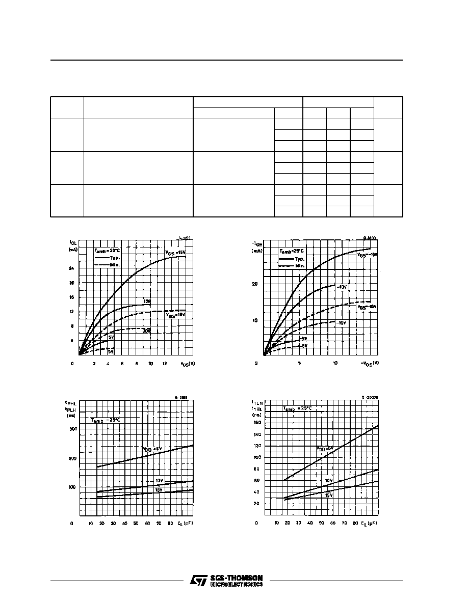
Output Low (sink) Current Characteristics.
Output High (source) Current Characteristics.
Typical Propagation Delay Time (P, G In to P, G
Out and Carry-outs) vs. Load Capacitance.
Typical Transition Time vs. Load Capacitance.
HCC/HCF40182B
5/12
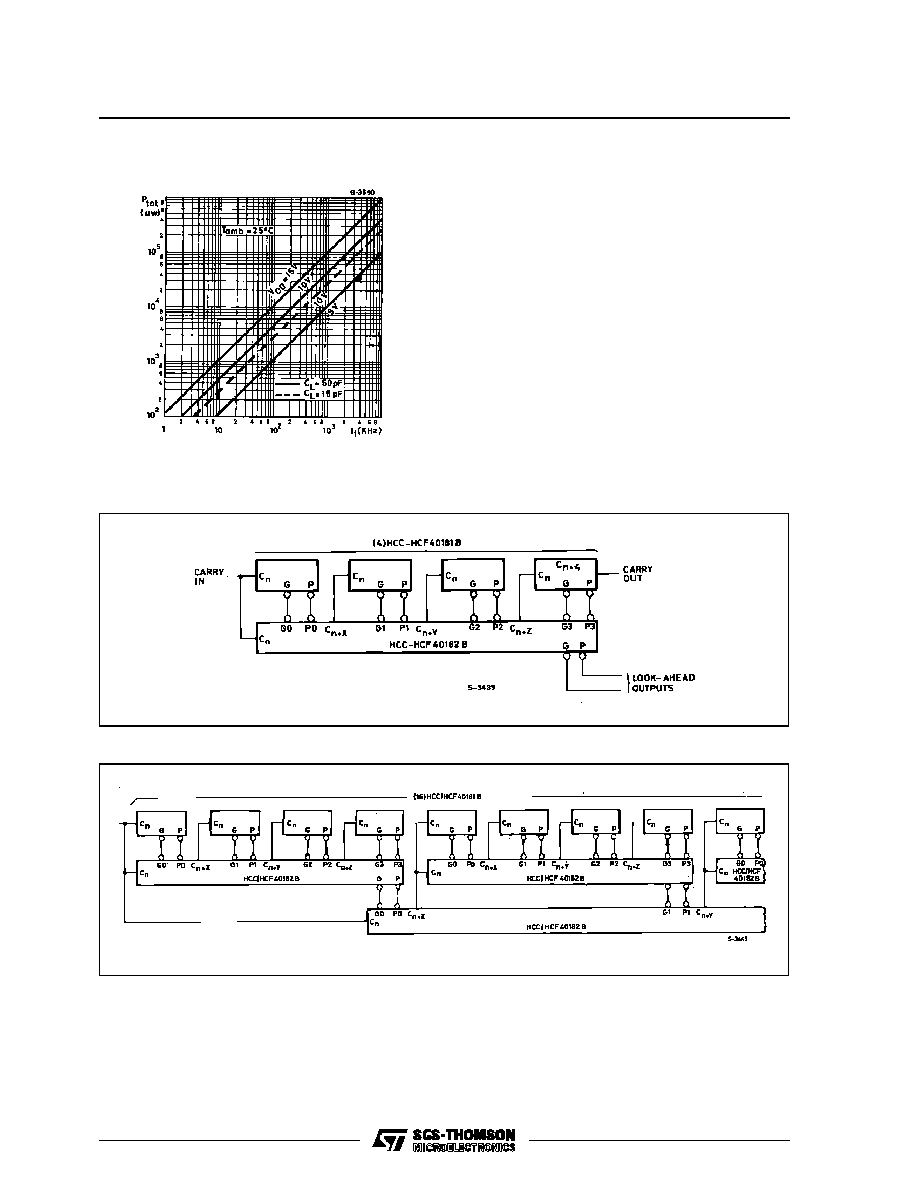
TYPICAL APPLICATIONS
16-BIT TWO-LEVEL LOOK-AHEAD ALU
64-BIT FULL CARRY LOOK-AHEAD ALU IN 3 LEVELS
Typical Dynamic Power Dissipation vs. Input Fre-
quency.
HCC/HCF40182B
6/12

TEST CIRCUITS
Quiescent Device Current.
Input Voltage.
COMBINED TWO-LEVEL LOOK-AHEAD AND RIPPLE-CARRY ALU
Input Leakage Current.
Dynamic Power Dissipation.
TYPICAL APPLICATIONS (continued)
HCC/HCF40182B
7/12

Plastic DIP16 (0.25) MECHANICAL DATA
DIM.
mm
inch
MIN.
TYP.
MAX.
MIN.
TYP.
MAX.
a1
0.51
0.020
B
0.77
1.65
0.030
0.065
b
0.5
0.020
b1
0.25
0.010
D
20
0.787
E
8.5
0.335
e
2.54
0.100
e3
17.78
0.700
F
7.1
0.280
I
5.1
0.201
L
3.3
0.130
Z
1.27
0.050
P001C
HCC/HCF40182B
8/12
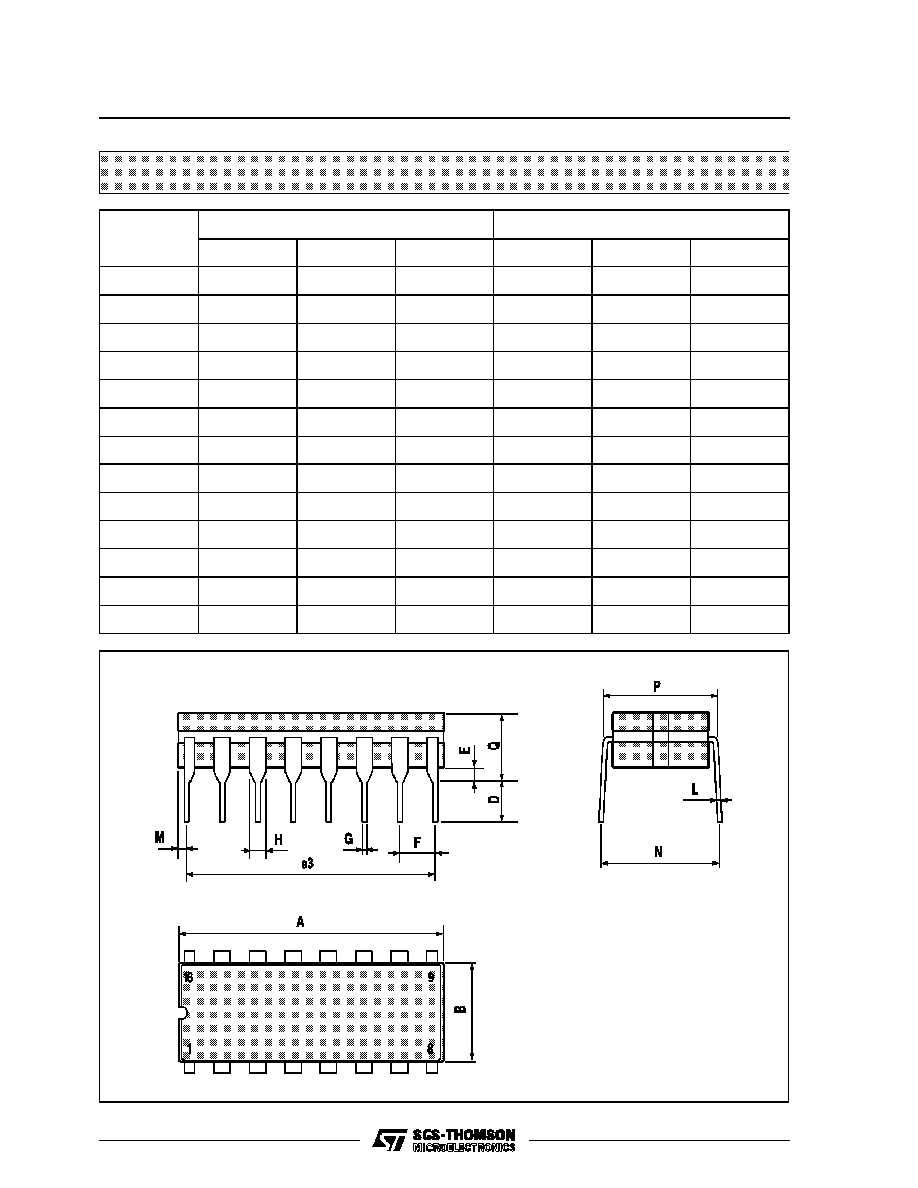
Ceramic DIP16/1 MECHANICAL DATA
DIM.
mm
inch
MIN.
TYP.
MAX.
MIN.
TYP.
MAX.
A
20
0.787
B
7
0.276
D
3.3
0.130
E
0.38
0.015
e3
17.78
0.700
F
2.29
2.79
0.090
0.110
G
0.4
0.55
0.016
0.022
H
1.17
1.52
0.046
0.060
L
0.22
0.31
0.009
0.012
M
0.51
1.27
0.020
0.050
N
10.3
0.406
P
7.8
8.05
0.307
0.317
Q
5.08
0.200
P053D
HCC/HCF40182B
9/12
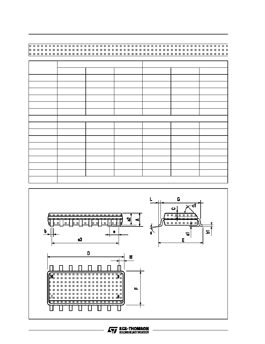
SO16 (Narrow) MECHANICAL DATA
DIM.
mm
inch
MIN.
TYP.
MAX.
MIN.
TYP.
MAX.
A
1.75
0.068
a1
0.1
0.2
0.004
0.007
a2
1.65
0.064
b
0.35
0.46
0.013
0.018
b1
0.19
0.25
0.007
0.010
C
0.5
0.019
c1
45
∞
(typ.)
D
9.8
10
0.385
0.393
E
5.8
6.2
0.228
0.244
e
1.27
0.050
e3
8.89
0.350
F
3.8
4.0
0.149
0.157
G
4.6
5.3
0.181
0.208
L
0.5
1.27
0.019
0.050
M
0.62
0.024
S
8
∞
(max.)
P013H
HCC/HCF40182B
10/12

PLCC20 MECHANICAL DATA
DIM.
mm
inch
MIN.
TYP.
MAX.
MIN.
TYP.
MAX.
A
9.78
10.03
0.385
0.395
B
8.89
9.04
0.350
0.356
D
4.2
4.57
0.165
0.180
d1
2.54
0.100
d2
0.56
0.022
E
7.37
8.38
0.290
0.330
e
1.27
0.050
e3
5.08
0.200
F
0.38
0.015
G
0.101
0.004
M
1.27
0.050
M1
1.14
0.045
P027A
HCC/HCF40182B
11/12

Information furnished is believed to be accurate and reliable. However, SGS-THOMSON Microelectronics assumes no responsability for the
consequences of use of such information nor for any infringement of patents or other rights of third parties which may results from its use. No
license is granted by implication or otherwise under any patent or patent rights of SGS-THOMSON Microelectronics. Specifications mentioned
in this publication are subject to change without notice. This publication supersedes and replaces all information previously supplied.
SGS-THOMSON Microelectronics products are not authorized for use as critical components in life support devices or systems without express
written approval of SGS-THOMSON Microelectonics.
©
1994 SGS-THOMSON Microelectronics - All Rights Reserved
SGS-THOMSON Microelectronics GROUP OF COMPANIES
Australia - Brazil - France - Germany - Hong Kong - Italy - Japan - Korea - Malaysia - Malta - Morocco - The Netherlands -
Singapore - Spain - Sweden - Switzerland - Taiwan - Thailand - United Kingdom - U.S.A
HCC/HCF40182B
12/12