
HCC/HCF40192B
HCC/HCF40193B
June 1989
WITH RESET) 40192B ≠ BCD TYPE 40193B ≠ BINARY TYPE
PRESETTABLE UP/DOWN COUNTERS (DUAL CLOCK
.
INDIVIDUAL CLOCK LINES FOR COUNTING
UP OR COUNTING DOWN
.
SYNCHRONOUS HIGH-SPEED CARRY AND
BORROW PROPAGATION DELAYS FOR CAS-
CADING
.
ASYNCHRONOUS RESET AND PRESET CA-
PABILITY
.
MEDIUM-SPEED OPERATION - f
CL
= 8MHz
(typ.) @ 10V
.
STANDARDIZED
SYMMETRICAL
OUTPUT
CHARACTERISTICS
.
5V, 10V, AND 15V PARAMETRIC RATINGS
.
INPUT CURRENT OF 100nA AT 18V AND 25
∞
C
FOR HCC DEVICE
.
100% TESTED FOR QUIESCENT CURRENT
.
MEETS ALL REQUIREMENTS OF JEDEC TEN-
TATIVE STANDARD N
∞
13A, "STANDARD SPE-
CIFICATIONS FOR DESCRIPTION OF "B"
SERIES CMOS DEVICES"
DESCRIPTION
The HCC40192B, HCC40193B, (extended tem-
perature range) and the HCF40192B, HCF40193B
(intermediate temperature range) are monolithic in-
tegrated circuits, available in 16-lead dual in-line
plastic or ceramic package and platic micro pack-
age. The HCC/HCF40192B Presettable BCD
Up/Down Counter and the HCC/HCF40193B Pres-
ettable Binary Up/Down Counter each consist of 4
synchronously clocked, gated "D" type flip-flops
connected as a counter. The inputs consist of 4 in-
dividual jam lines, a PRESET ENABLE control, in-
dividual CLOCK UP and CLOCK DOWN signals
and a master RESET. Four buffered Q signal out-
puts as well as CARRY and BORROW outputs for
multiple-stage counting schemes are provided. The
counter is cleared so that all outputs are in a low
state by a high on the RESET line. A RESET is ac-
complished asynchronously with the clock. Each
output is individually programmable asynchron-
ously with the clock to the level on the corresponding
jam input when thePRESET ENABLE control is low.
The counter counts up one count on the positive
clock edge of the CLOCK UP signal provided the
CLOCK DOWN line is high. The counter counts
down one count on the positive clock edge of the
CLOCK DOWN signal provided the CLOCK UP line
EY
(Plastic Package)
F
(Ceramic Frit Seal Package)
C1
(Plastic Chip Carrier)
ORDER CODES :
HCC401XXBF
HCF401XXBM1
HCF401XXBEY
HCF401XXBC1
PIN CONNECTIONS
M1
(Chip Carrier)
1/15
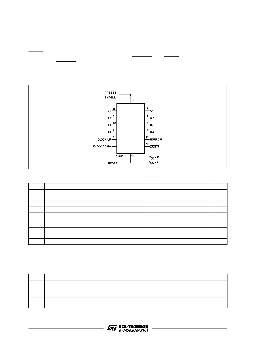
is high. The CARRY and BORROW signals are high
when the counter is counting up or down. The
CARRY signal goes low one-half clock cycle after
the counter reaches its maximum count in the count-
up mode. The BORROW signal goes low one-half
clock cycle after the counter reaches its minimum
count in the count-down mode. Cascading of
multiple packages is easily accomplished without
the need for additional external circuitry by tying the
BORROW and CARRY outputs to the CLOCK
DOWN and CLOCK UP inputs, respectively, of the
succeeding package.
FUNCTIONAL DIAGRAM
ABSOLUTE MAXIMUM RATINGS
Symbol
Parameter
Value
Unit
V
DD
*
Supply Voltage : HC C Types
H C F Types
≠ 0.5 to + 20
≠ 0.5 to + 18
V
V
V
i
Input Voltage
≠ 0.5 to V
DD
+ 0.5
V
I
I
DC Input Current (any one input)
±
10
mA
P
t o t
Total Power Dissipation (per package)
Dissipation per Output Transistor
for T
o p
= Full Package-temperature Range
200
100
mW
mW
T
o p
Operating Temperature : HCC Types
H CF Types
≠ 55 to + 125
≠ 40 to + 85
∞
C
∞
C
T
s t g
Storage Temperature
≠ 65 to + 150
∞
C
Stresses above those listed under "Absolute Maximum Ratings" may cause permanent damage to the device. This is a stress
rating only and functional operation of the device at these or any other conditions above those indicated in the operational sections
of this specification is not implied. Exposure to absolute maximum rating conditions for external periods may affect device reliability.
* All voltages are with respect to V
SS
(GND).
RECOMMENDED OPERATING CONDITIONS
Symbol
Parameter
Value
Unit
V
DD
Supply Voltage : H CC Types
H C F Types
3 to 18
3 to 15
V
V
V
I
Input Voltage
0 to V
DD
V
T
o p
Operating Temperature : HCC Types
H CF Types
≠ 55 to + 125
≠ 40 to + 85
∞
C
∞
C
HCC/HCF40192B/193B
2/15


