1/9
September 2001
s
MEDIUM-SPEED OPERATION
t
PD
= 60ns (Typ.) at V
DD
= 10V
s
QUIESCENT CURRENT SPECIFIED UP TO
20V
s
STANDARDIZED SYMMETRICAL OUTPUT
CHARACTERISTICS
s
5V, 10V AND 15V PARAMETRIC RATINGS
s
INPUT LEAKAGE CURRENT
I
I
= 100nA (MAX) AT V
DD
= 18V T
A
= 25°C
s
100% TESTED FOR QUIESCENT CURRENT
s
MEETS ALL REQUIREMENTS OF JEDEC
JESD13B " STANDARD SPECIFICATIONS
FOR DESCRIPTION OF B SERIES CMOS
DEVICES"
DESCRIPTION
The HCF4019B is a monolithic integrated circuit
fabricated in Metal Oxide Semiconductor
technology available in DIP and SOP packages.
The HCF4019B types are comprised of four AND/
OR select gate configurations, each consisting of
two 2 input AND gates driving a single 2-input OR
gate. Selection is accomplished by control bits K
a
and K
b
. In addition to selection of either channel A
or channel B information, the control bits can be
applied simultaneously to accomplish the logical
A+B function.
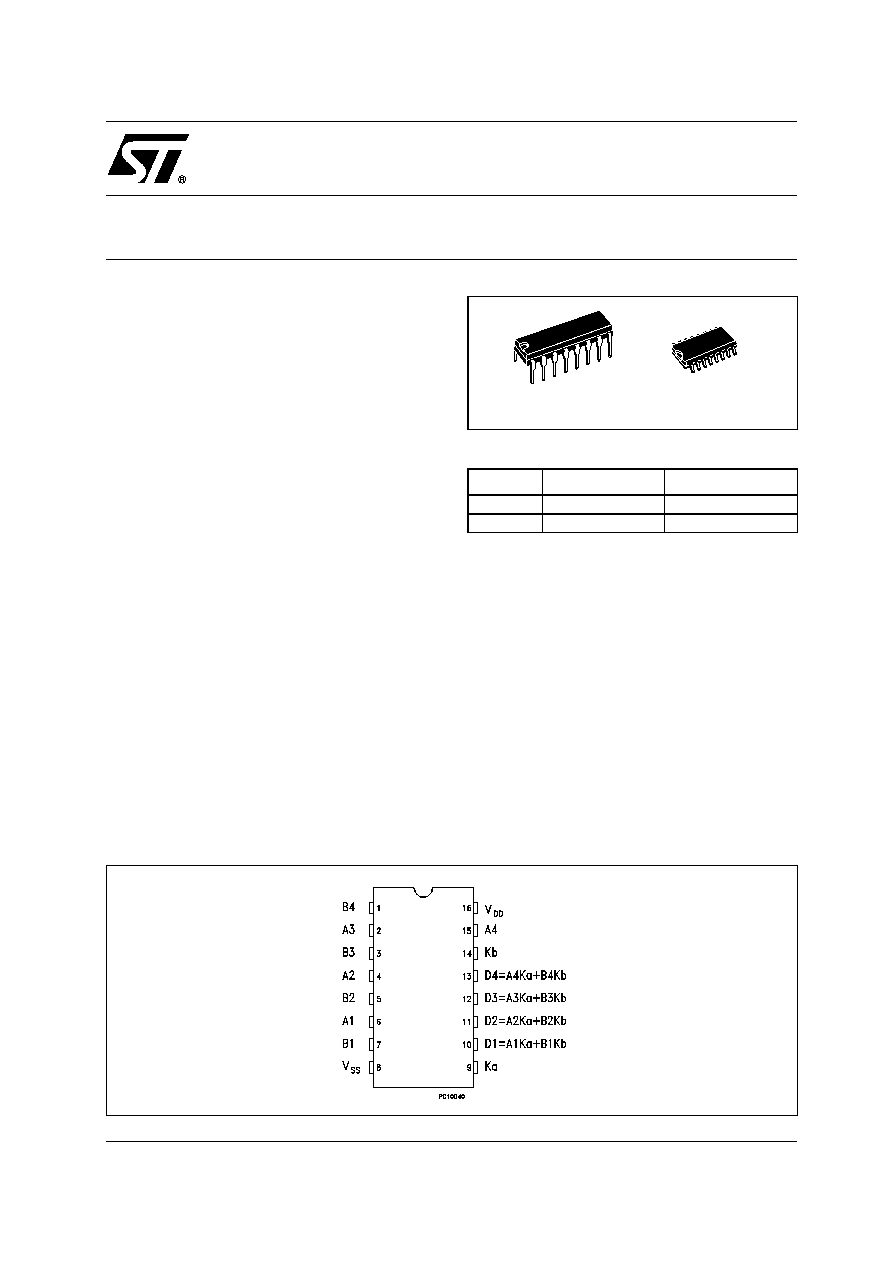
HCF4019B
QUAD AND/OR SELECT GATE
PIN CONNECTION
ORDER CODES
PACKAGE
TUBE
T & R
DIP
HCF4019BEY
SOP
HCF4019BM1
HCF4019M013TR
DIP
SOP
HCF4019B
2/9
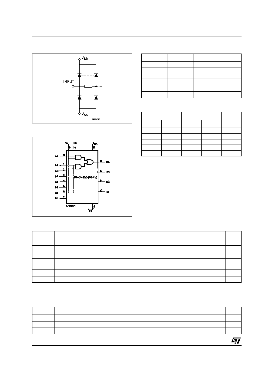
INPUT EQUIVALENT CIRCUIT
LOGIC DIAGRAM
PIN DESCRIPTION
TRUTH TABLE
X : Don"t Care
ABSOLUTE MAXIMUM RATINGS
Absolute Maximum Ratings are those values beyond which damage to the device may occur. Functional operation under these conditions is
not implied.
All voltage values are referred to V
SS
pin voltage.
RECOMMENDED OPERATING CONDITIONS
PIN No
SYMBOL
NAME AND FUNCTION
6, 4, 2, 15
A1 to A4
Data Inputs
7, 5, 3, 1
B1 to B4
Data inputs
10, 11,12, 13
D1 to D4
Data Outputs
9, 14
K
a
, K
b
Control bits
8
V
SS
Negative Supply Voltage
16
V
DD
Positive Supply Voltage
CONTROL
INPUTS
OUTPUT
Ka
Kb
A1 to A4
B1 to B4
D1 to D4
H
X
H
X
H
H
X
L
X
L
X
H
X
H
H
X
H
X
L
L
L
L
X
X
L
Symbol
Parameter
Value
Unit
V
DD
Supply Voltage
-0.5 to +22
V
V
I
DC Input Voltage
-0.5 to V
DD
+ 0.5
V
I
I
DC Input Current
±
10
mA
P
D
Power Dissipation per Package
200
mW
Power Dissipation per Output Transistor
100
mW
T
op
Operating Temperature
-55 to +125
°C
T
stg
Storage Temperature
-65 to +150
°C
Symbol
Parameter
Value
Unit
V
DD
Supply Voltage
3 to 20
V
V
I
Input Voltage
0 to V
DD
V
T
op
Operating Temperature
-55 to 125
°C
HCF4019B
3/9
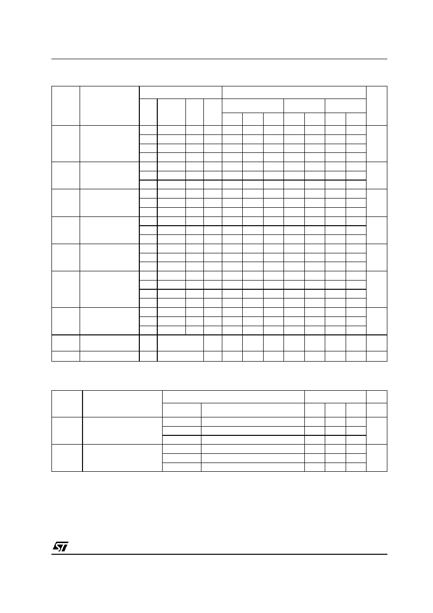
DC SPECIFICATIONS
The Noise Margin for both "1" and "0" level is: 1V min. with V
DD
=5V, 2V min. with V
DD
=10V, 2.5V min. with V
DD
=15V
DYNAMIC ELECTRICAL CHARACTERISTICS (T
amb
= 25°C, C
L
= 50pF, R
L
= 200K
, t
r
= t
f
= 20 ns)
(*) Typical temperature coefficient for all V
DD
value is 0.3 %/°C.
Symbol
Parameter
Test Condition
Value
Unit
V
I
(V)
V
O
(V)
|I
O
|
(
µ
A)
V
DD
(V)
T
A
= 25°C
-40 to 85°C
-55 to 125°C
Min.
Typ.
Max.
Min.
Max.
Min.
Max.
I
L
Quiescent Current
0/5
5
0.02
1
30
30
µ
A
0/10
10
0.02
2
60
60
0/15
15
0.02
4
120
120
0/20
20
0.04
20
600
600
V
OH
High Level Output
Voltage
0/5
<1
5
4.95
4.95
4.95
V
0/10
<1
10
9.95
9.95
9.95
0/15
<1
15
14.95
14.95
14.95
V
OL
Low Level Output
Voltage
5/0
<1
5
0.05
0.05
0.05
V
10/0
<1
10
0.05
0.05
0.05
15/0
<1
15
0.05
0.05
0.05
V
IH
High Level Input
Voltage
0.5/4.5
<1
5
3.5
3.5
3.5
V
1/9
<1
10
7
7
7
1.5/13.5
<1
15
11
11
11
V
IL
Low Level Input
Voltage
4.5/0.5
<1
5
1.5
1.5
1.5
V
9/1
<1
10
3
3
3
13.5/1.5
<1
15
4
4
4
I
OH
Output Drive
Current
0/5
2.5
<1
5
-1.36
-3.2
-1.15
-1.1
mA
0/5
4.6
<1
5
-0.44
-1
-0.36
-0.36
0/10
9.5
<1
10
-1.1
-2.6
-0.9
-0.9
0/15
13.5
<1
15
-3.0
-6.8
-2.4
-2.4
I
OL
Output Sink
Current
0/5
0.4
<1
5
0.44
1
0.36
0.36
mA
0/10
0.5
<1
10
1.1
2.6
0.9
0.9
0/15
1.5
<1
15
3.0
6.8
2.4
2.4
I
I
Input Leakage
Current
0/18
Any Input
18
±
10
-5
±
0.1
±
1
±
1
µ
A
C
I
Input Capacitance
Any Input
5
7.5
pF
Symbol
Parameter
Test Condition
Value (*)
Unit
V
DD
(V)
Min.
Typ.
Max.
t
PLH
t
PHL
Propagation Delay Time
5
150
300
ns
10
60
120
15
50
100
t
TLH
t
THL
Output Transition Time
5
100
200
ns
10
50
100
15
40
80