
1/11
September 2001
s
MEDIUM SPEED OPERATION :
10 MHz (Typ.) at V
DD
= 10V
s
FULLY STATIC OPERATION
s
STANDARDIZED SYMMETRICAL OUTPUT
CHARACTERISTICS
s
QUIESCENT CURRENT SPECIFIED UP TO
20V
s
5V, 10V AND 15V PARAMETRIC RATINGS
s
INPUT LEAKAGE CURRENT
I
I
= 100nA (MAX) AT V
DD
= 18V T
A
= 25∞C
s
100% TESTED FOR QUIESCENT CURRENT
s
MEETS ALL REQUIREMENTS OF JEDEC
JESD13B " STANDARD SPECIFICATIONS
FOR DESCRIPTION OF B SERIES CMOS
DEVICES"
DESCRIPTION
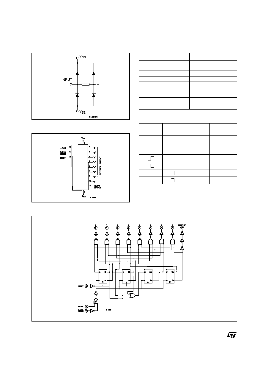
The HCF4022B is a monolithic integrated circuit
fabricated in Metal Oxide Semiconductor
technology available in DIP and SOP packages.
The HCF4022B is 4-stage Johnson counter
having 8 decoded outputs. Inputs include a
CLOCK, a RESET, and a CLOCK INHIBIT signal.
Schmitt trigger action in the clock input circuit
provides pulse shaping that allows unlimited clock
input pulse rise and fall times. This counter is
advanced one count at the positive clock signal
transition if the CLOCK INHIBIT signal is low.
Counter advanced via the clock line is inhibited
when the CLOCK INHIBIT signal is high. A high
RESET signal clears the counter to its zero count.
Use of the Johnson decade-counter configuration
permits high speed operation, 2-input decimal
decode gating and spike-free decoded outputs.
Anti-lock gating is provided, thus assuring proper
counting sequence. The decoded outputs are
normally low and go high only at their respective
decoded time slot. Each decoded output remains
high for one full clock cycle. A CARRY - OUT
signal completes one cycle every 8 clock input
cycles and is used to ripple-clock the succeeding
device in a multi-device counting chain.
HCF4022B
OCTAL COUNTER WITH 8 DECODED OUTPUTS
PIN CONNECTION
ORDER CODES
PACKAGE
TUBE
T & R
DIP
HCF4022BEY
SOP
HCF4022BM1
HCF4022M013TR
DIP
SOP
HCF4022B
2/11
INPUT EQUIVALENT CIRCUIT
FUNCTIONAL DIAGRAM
PIN DESCRIPTION
TRUTH TABLE
X : Don't Care
Qn : No Change
LOGIC DIAGRAM
This logic diagram has not be used to estimate propagation delays
PIN No
SYMBOL
NAME AND FUNCTION
2, 1, 3, 7, 11,
4, 5, 10
0 to 7
Decoded Output
6, 9
NC
Not Connected
14
CLOCK
Clock Input
13
CLOCK
INHIBIT
Clock Inhibit Input
15
RESET
Reset Input
12
CARRY OUT Carry Output
8
V
SS
Negative Supply Voltage
CLOCK
CLOCK
INHIBIT
RESET
DECODED
OUTPUT
X
X
H
Q
0
L
X
L
Q
n
X
H
L
Q
n
L
L
Q
n+1
L
L
Q
n
H
L
Q
n
H
L
Q
n+1

HCF4022B
3/11
TIMING CHART
ABSOLUTE MAXIMUM RATINGS
Absolute Maximum Ratings are those values beyond which damage to the device may occur. Functional operation under these conditions is
not implied.
All voltage values are referred to V
SS
pin voltage.
RECOMMENDED OPERATING CONDITIONS
Symbol
Parameter
Value
Unit
V
DD
Supply Voltage
-0.5 to +22
V
V
I
DC Input Voltage
-0.5 to V
DD
+ 0.5
V
I
I
DC Input Current
±
10
mA
P
D
Power Dissipation per Package
200
mW
Power Dissipation per Output Transistor
100
mW
T
op
Operating Temperature
-55 to +125
∞C
T
stg
Storage Temperature
-65 to +150
∞C
Symbol
Parameter
Value
Unit
V
DD
Supply Voltage
3 to 20
V
V
I
Input Voltage
0 to V
DD
V
T
op
Operating Temperature
-55 to 125
∞C
HCF4022B
4/11
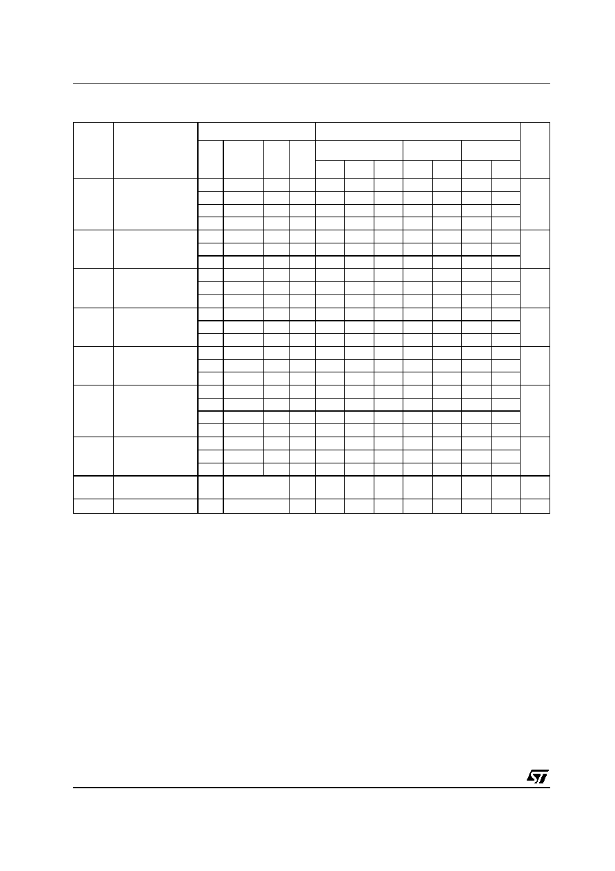
DC SPECIFICATIONS
The Noise Margin for both "1" and "0" level is: 1V min. with V
DD
=5V, 2V min. with V
DD
=10V, 2.5V min. with V
DD
=15V
Symbol
Parameter
Test Condition
Value
Unit
V
I
(V)
V
O
(V)
|I
O
|
(
µ
A)
V
DD
(V)
T
A
= 25∞C
-40 to 85∞C
-55 to 125∞C
Min.
Typ.
Max.
Min.
Max.
Min.
Max.
I
L
Quiescent Current
0/5
5
0.04
5
150
150
µ
A
0/10
10
0.04
10
300
300
0/15
15
0.04
20
600
600
0/20
20
0.08
100
3000
3000
V
OH
High Level Output
Voltage
0/5
<1
5
4.95
4.95
4.95
V
0/10
<1
10
9.95
9.95
9.95
0/15
<1
15
14.95
14.95
14.95
V
OL
Low Level Output
Voltage
5/0
<1
5
0.05
0.05
0.05
V
10/0
<1
10
0.05
0.05
0.05
15/0
<1
15
0.05
0.05
0.05
V
IH
High Level Input
Voltage
0.5/4.5
<1
5
3.5
3.5
3.5
V
1/9
<1
10
7
7
7
1.5/13.5
<1
15
11
11
11
V
IL
Low Level Input
Voltage
4.5/0.5
<1
5
1.5
1.5
1.5
V
9/1
<1
10
3
3
3
13.5/1.5
<1
15
4
4
4
I
OH
Output Drive
Current
0/5
2.5
<1
5
-1.36
-3.2
-1.1
-1.1
mA
0/5
4.6
<1
5
-0.44
-1
-0.36
-0.36
0/10
9.5
<1
10
-1.1
-2.6
-0.9
-0.9
0/15
13.5
<1
15
-3.0
-6.8
-2.4
-2.4
I
OL
Output Sink
Current
0/5
0.4
<1
5
0.44
1
0.36
0.36
mA
0/10
0.5
<1
10
1.1
2.6
0.9
0.9
0/15
1.5
<1
15
3.0
6.8
2.4
2.4
I
I
Input Leakage
Current
0/18
Any Input
18
±
10
-5
±
0.1
±
1
±
1
µ
A
C
I
Input Capacitance
Any Input
5
7.5
pF
HCF4022B
5/11
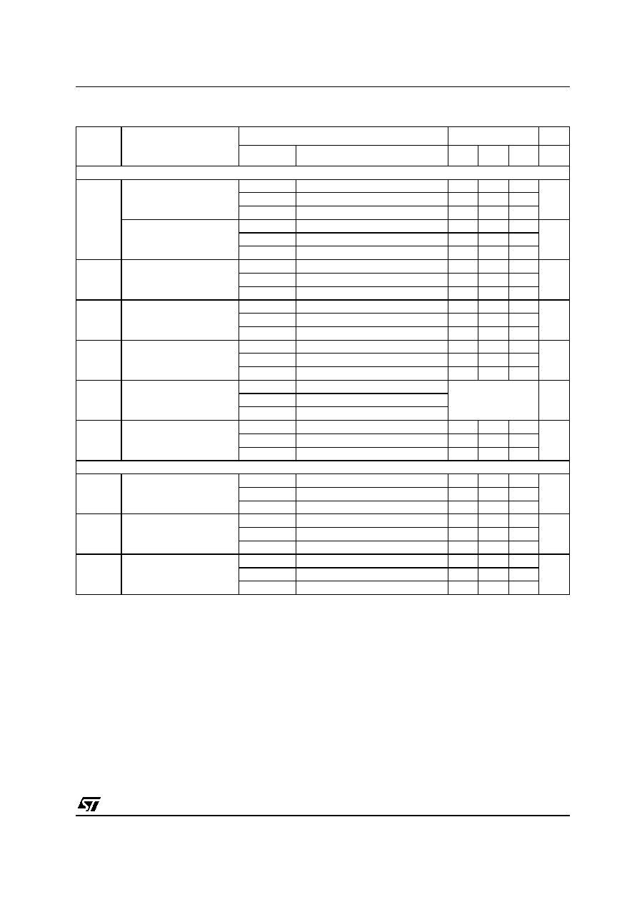
DYNAMIC ELECTRICAL CHARACTERISTICS (T
amb
= 25∞C, C
L
= 50pF, R
L
= 200K
, t
r
= t
f
= 20 ns)
(*) Typical temperature coefficient for all V
DD
value is 0.3 %/∞C.
(1) Measured with respect to carry out line.
Symbol
Parameter
Test Condition
Value (*)
Unit
V
DD
(V)
Min.
Typ.
Max.
CLOCKED OPERATION
t
PLH
t
PHL
Propagation Delay Time
(decode out)
5
325
650
ns
10
135
270
15
85
170
Propagation Delay Time
(carry out)
5
300
600
ns
10
125
250
15
80
160
t
THL
t
TLH
Transition Time (carry out
or decoded out lines)
5
100
200
ns
10
50
100
15
40
80
f
CL
(1)
Maximum Clock Input
Frequency
5
2.5
5
5
MHz
10
5
10
15
5.5
11
t
W
Minimum Clock Pulse
Width
5
100
200
ns
10
45
90
15
30
60
t
r
, t
f
Clock Input Rise or Fall
Time
5
unlimited
µ
s
10
15
t
setup
Data Setup Time Minimum
Clock Inhibit
5
115
230
ns
10
50
100
15
35
75
RESET OPERATION
t
PLH,
t
PHL
Propagation Delay Time
(carry out or decoded out
lines)
5
265
530
ns
10
115
230
15
85
170
t
W
Minimum Reset Pulse
Width
5
130
260
ns
10
55
110
15
30
60
t
REM
Minimum Reset Removal
Time
5
200
400
ns
10
140
280
15
75
150