 | –≠–ª–µ–∫—Ç—Ä–æ–Ω–Ω—ã–π –∫–æ–º–ø–æ–Ω–µ–Ω—Ç: HCF4028 | –°–∫–∞—á–∞—Ç—å:  PDF PDF  ZIP ZIP |
1/10
September 2002
s
BCD TO DECIMAL DECODING OR BINARY
TO OCTAL DECODING
s
HIGH DECODED OUTPUT DRIVE
CAPABILITY
s
"POSITIVE LOGIC" INPUTS AND OUTPUTS:
DECODED OUTPUTS GO HIGH ON
SELECTION
s
MEDIUM SPEED OPERATION : t
PHL
, t
PLH
=
80ns (Typ.) at V
DD
= 10V
s
QUIESCENT CURRENT SPECIF. UP TO 20V
s
STANDARDIZED SYMMETRICAL OUTPUT
CHARACTERISTICS
s
INPUT LEAKAGE CURRENT
I
I
= 100nA (MAX) AT V
DD
= 18V T
A
= 25∞C
s
100% TESTED FOR QUIESCENT CURRENT
s
MEETS ALL REQUIREMENTS OF JEDEC
JESD13B "STANDARD SPECIFICATIONS
FOR DESCRIPTION OF B SERIES CMOS
DEVICES"
DESCRIPTION
HCF4028B is a monolithic integrated circuit
fabricated in Metal Oxide Semiconductor
technology available in DIP and SOP packages.
HCF4028B is a BCD to DECIMAL or BINARY to
OCTAL decoder consisting of buffering on all 4
inputs, decoding logic gates, and 10 output
buffers.
A BCD code applied to the four inputs, A to D,
results in a high level at the selected one of 10
decimal decoded outputs. Similarly, a 3-bit binary
code applied to inputs A through C is decoded in
octal code at output 0 to 7 if D = "0". High drive
capability is provided at all outputs to enhance dc
and dynamic performance in high fan-out
applications.
HCF4028B
BCD TO DECIMAL DECODER
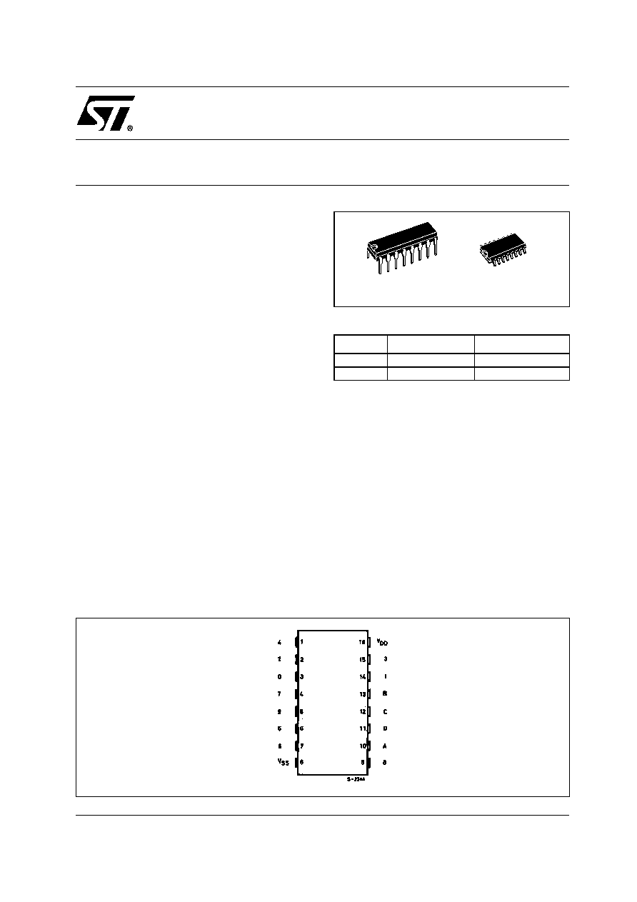
PIN CONNECTION
ORDER CODES
PACKAGE
TUBE
T & R
DIP
HCF4028BEY
SOP
HCF4028BM1
HCF4028M013TR
DIP
SOP

HCF4028B
2/10
IINPUT EQUIVALENT CIRCUIT
PIN DESCRIPTION
FUNCTIONAL DIAGRAM
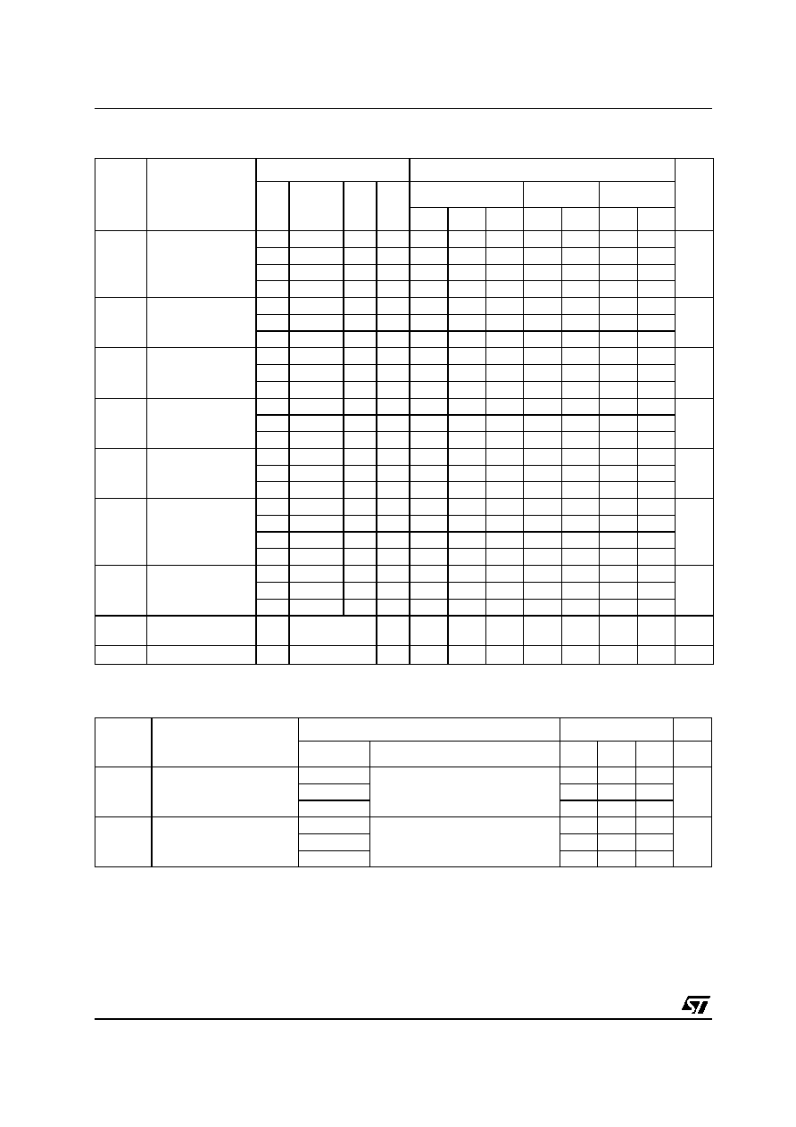
TRUTH TABLE
PIN No
SYMBOL
NAME AND FUNCTION
10, 13, 12,
11
A, B, C, D
BCD Data Inputs
10, 13, 12
A, B, C
3-Bit Binary Inputs
3, 14, 2, 15,
1, 6, 7, 4, 9,
5
0 to 9
Buffered DECIMAL
Decoded Outputs
3, 14, 2, 15,
1, 6, 7, 4
0 to 7
Buffered OCTAL Decoded
Outputs
8
V
SS
Negative Supply Voltage
16
V
DD
Positive Supply Voltage
INPUTS
OUTPUTS
D
C
B
A
0
1
2
3
4
5
6
7
8
9
L
L
L
L
H
L
L
L
L
L
L
L
L
L
L
L
L
H
L
H
L
L
L
L
L
L
L
L
L
L
H
L
L
L
H
L
L
L
L
L
L
L
L
L
H
H
L
L
L
H
L
L
L
L
L
L
L
H
L
L
L
L
L
L
H
L
L
L
L
L
L
H
L
H
L
L
L
L
L
H
L
L
L
L
L
H
H
L
L
L
L
L
L
L
H
L
L
L
L
H
H
H
L
L
L
L
L
L
L
H
L
L
H
L
L
L
L
L
L
L
L
L
L
L
H
L
H
L
L
H
L
L
L
L
L
L
L
L
L
H
H
L
H
L
L
L
L
L
L
L
L
L
L
L
H
L
H
H
L
L
L
L
L
L
L
L
L
L
H
H
L
L
L
L
L
L
L
L
L
L
L
L
H
H
L
H
L
L
L
L
L
L
L
L
L
L
H
H
H
L
L
L
L
L
L
L
L
L
L
L
H
H
H
H
L
L
L
L
L
L
L
L
L
L

HCF4028B
3/10
LOGIC DIAGRAM
ABSOLUTE MAXIMUM RATINGS
Absolute Maximum Ratings are those values beyond which damage to the device may occur. Functional operation under these conditions is
not implied.
All voltage values are referred to V
SS
pin voltage.
RECOMMENDED OPERATING CONDITIONS
Symbol
Parameter
Value
Unit
V
DD
Supply Voltage
-0.5 to +22
V
V
I
DC Input Voltage
-0.5 to V
DD
+ 0.5
V
I
I
DC Input Current
±
10
mA
P
D
Power Dissipation per Package
200
mW
Power Dissipation per Output Transistor
100
mW
T
op
Operating Temperature
-55 to +125
∞C
T
stg
Storage Temperature
-65 to +150
∞C
Symbol
Parameter
Value
Unit
V
DD
Supply Voltage
3 to 20
V
V
I
Input Voltage
0 to V
DD
V
T
op
Operating Temperature
-55 to 125
∞C
HCF4028B
4/10
DC SPECIFICATIONS
The Noise Margin for both "1" and "0" level is: 1V min. with V
DD
=5V, 2V min. with V
DD
=10V, 2.5V min. with V
DD
=15V
DYNAMIC ELECTRICAL CHARACTERISTICS (T
amb
= 25∞C, C
L
= 50pF, R
L
= 200K
, t
r
= t
f
= 20 ns)
(*) Typical temperature coefficient for all V
DD
value is 0.3 %/∞C.
Symbol
Parameter
Test Conditions
Value
Unit
V
I
(V)
V
O
(V)
I
O
(
µ
A)
V
DD
(V)
T
A
= 25∞C
-40 to 85∞C
-55 to 125∞C
Min.
Typ.
Max.
Min.
Max.
Min.
Max.
I
L
Quiescent Current
0/5
5
0.04
5
150
150
µ
A
0/10
10
0.04
10
300
300
0/15
15
0.04
20
600
600
0/20
20
0.08
100
3000
3000
V
OH
High Level Output
Voltage
0/5
<1
5
4.95
4.95
4.95
V
0/10
<1
10
9.95
9.95
9.95
0/15
<1
15
14.95
14.95
14.95
V
OL
Low Level Output
Voltage
5/0
<1
5
0.05
0.05
0.05
V
10/0
<1
10
0.05
0.05
0.05
15/0
<1
15
0.05
0.05
0.05
V
IH
High Level Input
Voltage
0.5/4.5
<1
5
3.5
3.5
3.5
V
1/9
<1
10
7
7
7
1.5/18.5
<1
15
11
11
11
V
IL
Low Level Input
Voltage
0.5/4.5
<1
5
1.5
1.5
1.5
V
9/1
<1
10
3
3
3
1.5/18.5
<1
15
4
4
4
I
OH
Output Drive
Current
0/5
2.5
5
-1.36
-3.2
-1.1
-1.1
mA
0/5
4.6
5
-0.44
-1
-0.36
-0.36
0/10
9.5
10
-1.1
-2.6
-0.9
-0.9
0/15
13.5
15
-3.0
-6.8
-2.4
-2.4
I
OL
Output Sink
Current
0/5
0.4
5
0.44
1
0.36
0.36
mA
0/10
0.5
10
1.1
2.6
0.9
0.9
0/15
1.5
15
3.0
6.8
2.4
2.4
I
I
Input Leakage
Current
0/18
any input
18
±
10
-5
±
0.1
±
1
±
1
µ
A
C
I
Input Capacitance
any input
5
7.5
pF
Symbol
Parameter
Test Condition
Value (*)
Unit
V
DD
(V)
Min.
Typ.
Max.
t
PHL
t
PLH
Propagation Delay Time
(Clock to "Out")
5
175
350
ns
10
80
160
15
60
120
t
THL
t
TLH
Transition Time
(Carry Out Line)
5
100
200
ns
10
50
100
15
25
50

HCF4028B
5/10
TEST CIRCUIT
C
L
= 50pF or equivalent (includes jig and probe capacitance)
R
L
= 200K
R
T
= Z
OUT
of pulse generator (typically 50
)
WAVEFORM : PROPAGATION DELAY TIMES (f=1MHz; 50% duty cycle)
TYPICAL APPLICATION
The circuit shown in fig. 1 converts any 4-bit code
to a decimal or hexadecimal code. Fig. 2 shows a
number of codes and the decimal or hexadecimal
number in these codes, which must be applied to
the input pins of HCF4028B to select a particular
output. For example: in order to get a "high" on
output 8 the input must be either an 8 expressed in
4-bit binary code or a 15 expressed in
excess-3code.