1/9
September 2001
s
INVERT INPUTS ON ALL ADDERS FOR
SUM COMPLEMENTING APPLICATIONS
s
FULLY STATIC OPERATION...DC TO 10MHz
(Typ.) at V
DD
= 10V
s
BUFFERED INPUTS AND OUTPUTS
s
SINGLE PHASE CLOCKING
s
QUIESCENT CURRENT SPECIFIED UP TO
20V
s
STANDARDIZED SYMMETRICAL OUTPUT
CHARACTERISTICS
s
INPUT LEAKAGE CURRENT
I
I
= 100nA (MAX) AT V
DD
= 18V T
A
= 25°C
s
100% TESTED FOR QUIESCENT CURRENT
s
MEETS ALL REQUIREMENTS OF JEDEC
JESD13B " STANDARD SPECIFICATIONS
FOR DESCRIPTION OF B SERIES CMOS
DEVICES"
DESCRIPTION
The HCF4032B is a monolithic integrated circuit
fabricated in Metal Oxide Semiconductor
technology available in DIP and SOP packages.
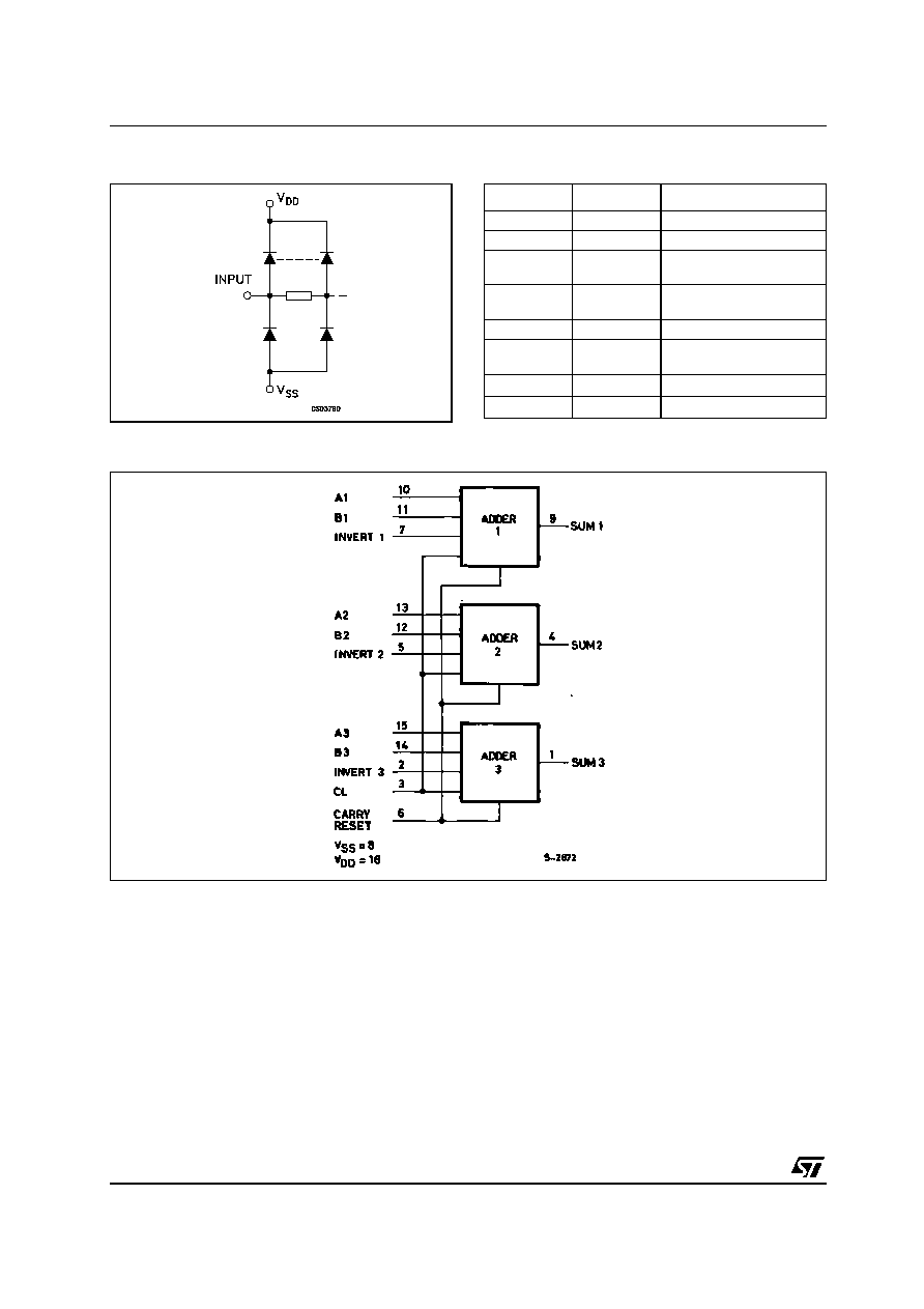
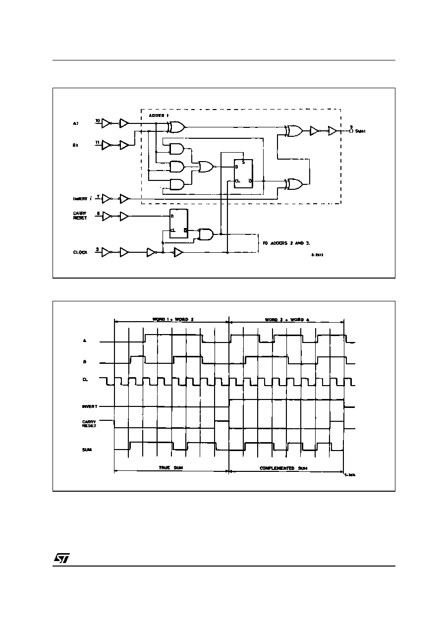
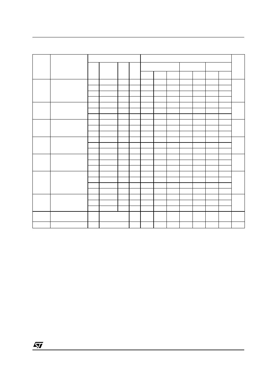
The HCF4032B consists of three serial adder
circuits with common CLOCK and
CARRY-RESET inputs. Each adder has two
provisions for two serial DATA INPUT signals and
an INVERT command signal. When the command
signal is a logical "1", the sum is complemented.
Data words enter the adder with the least
significant bit first; the sign bit trails. The output is
the MOD 2 sum of the input bits plus the carry
from the previous bit position. The carry is only
added at the positive going clock transition, thus,
for spike-free operation the input data transitions
should occur as soon as possible after the
triggering edge. The CARRY is reset to a logical
"0" at the end of each word by applying a logical
"1" signal to a CARRY-RESET input one bit
position before the application of the first bit of the
next word.
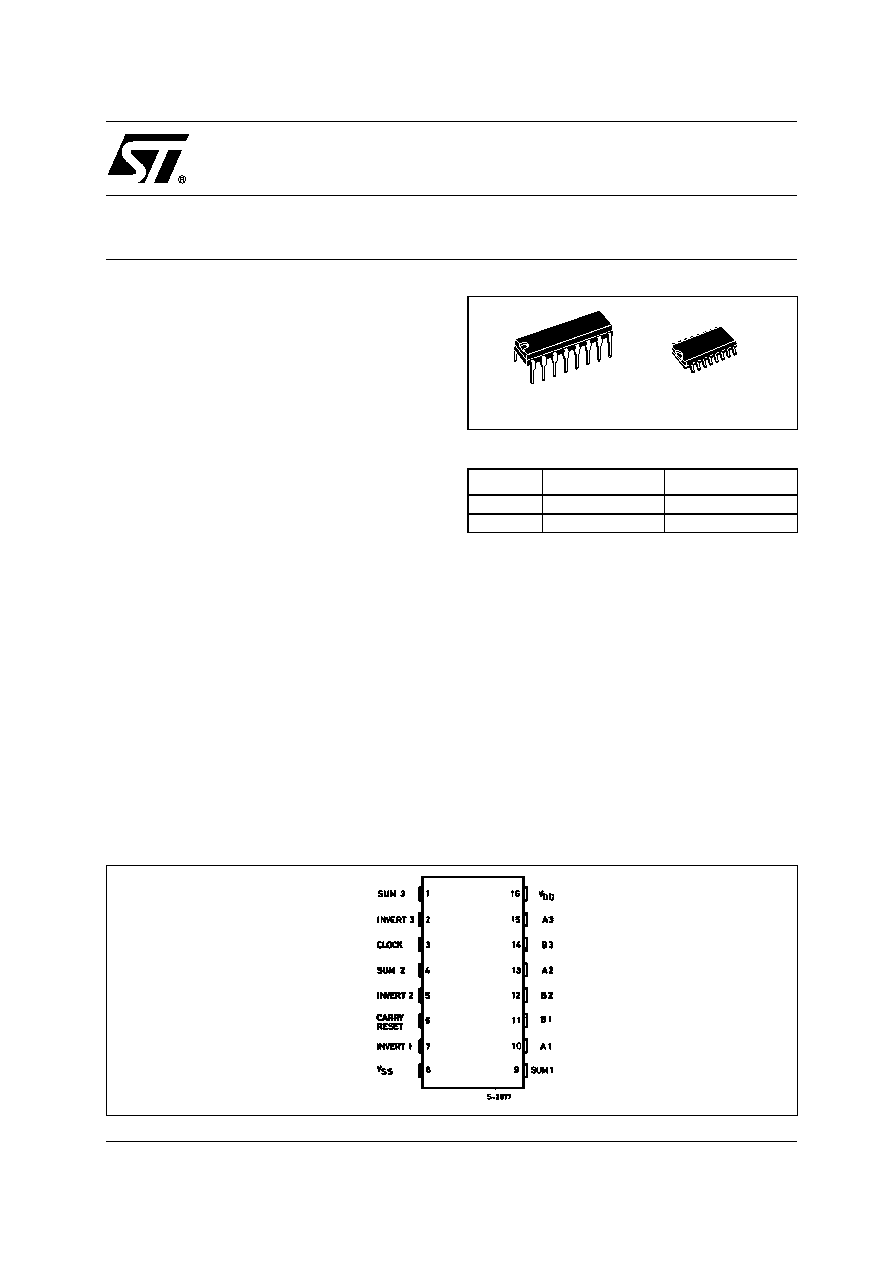
HCF4032B
TRIPLE SERIAL ADDER
PIN CONNECTION
ORDER CODES
PACKAGE
TUBE
T & R
DIP
HCF4032BEY
SOP
HCF4032BM1
HCF4032M013TR
DIP
SOP
HCF4032B
4/9
ABSOLUTE MAXIMUM RATINGS
Absolute Maximum Ratings are those values beyond which damage to the device may occur. Functional operation under these conditions is
not implied.
All voltage values are referred to V
SS
pin voltage.
RECOMMENDED OPERATING CONDITIONS
Symbol
Parameter
Value
Unit
V
DD
Supply Voltage
-0.5 to +22
V
V
I
DC Input Voltage
-0.5 to V
DD
+ 0.5
V
I
I
DC Input Current
±
10
mA
P
D
Power Dissipation per Package
200
mW
Power Dissipation per Output Transistor
100
mW
T
op
Operating Temperature
-55 to +125
°C
T
stg
Storage Temperature
-65 to +150
°C
Symbol
Parameter
Value
Unit
V
DD
Supply Voltage
3 to 20
V
V
I
Input Voltage
0 to V
DD
V
T
op
Operating Temperature
-55 to 125
°C