HCC/HCF4035B
July 1989
4-STAGE PARALLEL IN/PARALLEL OUT SHIFT REGISTER
.
4-STAGE CLOCKED SHIFT OPERATION
.
SYNCHRONOUS PARALLEL ENTRY ON ALL 4
STAGES
.
JK INPUTS ON FIRST STAGE
.
ASYNCHRONOUS TRUE/COMPLEMENT CON-
TROL ON ALL OUTPUTS
.
STATIC FLIP-FLOP OPERATION ; MASTER-
SLAVE CONFIGURATION
.
BUFFERED INPUTS AND OUTPUTS
.
HIGH SPEED 12MHz (typ.) AT V
DD
= 10V
.
QUIESCENT CURRENT SPECIFIED TO 20V
FOR HCC DEVICE
.
STANDARDIZED
SYMMETRICAL
OUTPUT
CHARACTERISTICS
.
5V, 10V, AND 15V PARAMETRIC RATINGS
.
INPUT CURR 100nA AT 18V AND 25
∞
C FOR
HCC DEVICE
.
100% TESTED FOR QUIESCENT CURRENT
.
MEETS ALL REQUIREMENTS OF JEDEC TEN-
TATIVE STANDARD N
∞
. 13A, "STANDARD
SPECIFICATIONS FOR DESCRIPTION OF "B"
SERIES CMOS DEVICES"
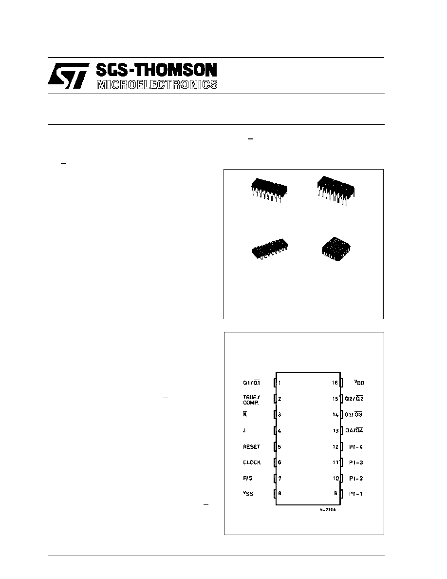
DESCRIPTION
The HCC4035B (extended temperature range) and
HCF4035B (intermediate temperature range) are
monolithic integrated circuit, available in 16-lead
dual in-line plastic or ceramic package and plastic
micro package. The HCC/HCF4035B is a four-
stage clocked signal serial register with provision for
synchronous PARALLEL inputs to each stage and
SERIAL inputs to the first stage via JK logic. Regis-
ter stages 2, 3, and 4 are coupled in a serial D flip-
flop configuration when the register is in the serial
mode (PARALLEL/SERIAL control low). Parallel
entry into each register stage is permitted when the
PARALLEL/SERIAL control is high. In the parallel or
serial mode information is transferred on positive
clock transitions. When the TRUE/COMPLEMENT
control is high, the true contents of the register are
available at the output terminals. When the
TRUE/COMPLEMENT control is low, the outputs
are the complements of the data in the register. The
TRUE/COMPLEMENT control functions asyn-
chronously with respect to the CLOCK signal. JK
input logic is provided on the first stage SERIAL
input to minimize logic requirements particularly in
counting and sequence-generation applications.
EY
(Plastic Package)
F
(Ceramic Frit Seal Package)
M1
(Micro Package)
C1
(Plastic Chip Carrier)
ORDER CODES :
HCC4035BF
HCF4035BM1
HCF4035BEY
HCF4035BC1
PIN CONNECTIONS
Whith JK inputs connected together, the first stage
becomes a D flip-flop. An asynchronous common
RESET is also provided.
1/14

ABSOLUTE MAXIMUM RATINGS
Symbol
Parameter
Value
Unit
V
DD
*
Supply Voltage : HC C Types
H C F Types
≠ 0.5 to + 20
≠ 0.5 to + 18
V
V
V
i
Input Voltage
≠ 0.5 to V
DD
+ 0.5
V
I
I
DC Input Current (any one input)
±
10
mA
P
t o t
Total Power Dissipation (per package)
Dissipation per Output Transistor
for T
o p
= Full Package-temperature Range
200
100
mW
mW
T
o p
Operating Temperature : HCC Types
H CF Types
≠ 55 to + 125
≠ 40 to + 85
∞
C
∞
C
T
s t g
Storage Temperature
≠ 65 to + 150
∞
C
Stresses above those listed under "Absolute Maximum Ratings" may cause permanent damage to the device. This is a stress rating only and
functional operation of the device at these or any other conditions above those indicated in the operational sections of this specification is not
implied. Exposure to absolute maximum rating conditions for external periods may affect device reliability.
* All voltage values are referred to V
SS
pin voltage.
FUNCTIONAL DIAGRAM
RECOMMENDED OPERATING CONDITIONS
Symbol
Parameter
Value
Unit
V
DD
Supply Voltage: HCC Types
HCF Types
3 to 18
3 to 15
V
V
V
I
Input Voltage
0 to V
DD
V
T
op
Operating Temperature: HCC Types
HCF Types
-55 to +125
-40 to +85
o
C
o
C
HCC/HCF4035B
2/14
LOGIC DIAGRAM
TRUTH TABLE
FIRST STAGE
t
n - 1
(inputs)
t
n
(outputs )
Clock
( ¯ )
J
K
R
Q
n - 1
Q
n
__
/
__
O
X
O
O
O
__
/
__
I
X
O
O
I
__
/
__
X
O
O
I
O
__
/
__
I
O
O
Q
n -1
Q
n - 1
____
Toggle
Mode
__
/
__
X
I
O
I
I
__
\__
X
X
O
Q
n -1
Q
n - 1
X
X
X
I
X
O
HCC/HCF4035B
3/14
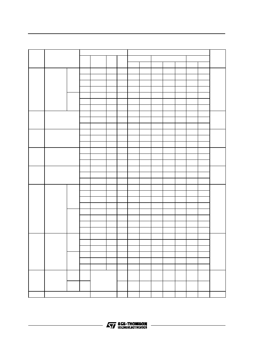
STATIC ELECTRICAL CHARACTERISTICS (over recommended operating conditions)
Test Conditions
Val ue
V
I
V
O
|I
O
|
V
D D
T
L o w
*
25
∞
C
T
Hi g h
*
Symbol
Parameter
(V)
(V)
(
µ
A)
(V)
Mi n. Max. Min.
Typ. Max. Min. Max.
Unit
I
L
Quiescent
Current
HCC
Types
0/ 5
5
5
0.04
5
150
µ
A
0/10
10
10
0.04
10
300
0/15
15
20
0.04
20
600
0/20
20
100
0.08
100
3000
HCF
Types
0/ 5
5
20
0.04
20
150
0/10
10
40
0.04
40
300
0/15
15
80
0.4
80
600
V
O H
Output High
Voltage
0/ 5
< 1
5
4.95
4.95
4.95
V
0/10
< 1
10
9.95
9.95
9.95
0/15
< 1
15
14.95
14.95
14.95
V
O L
Output Low
Voltage
5/0
< 1
5
0.05
0.05
0.05
V
10/0
< 1
10
0.05
0.05
0.05
15/0
< 1
15
0.05
0.05
0.05
V
IH
Input High
Voltage
0.5/4.5
< 1
5
3.5
3.5
3.5
V
1/9
< 1
10
7
7
7
1.5/13.5
< 1
15
11
11
11
V
IL
Input Low
Voltage
4.5/0.5
< 1
5
1.5
1.5
1.5
V
9/1
< 1
10
3
3
3
13.5/1.5
< 1
15
4
4
4
I
O H
Output
Drive
Current
HCC
Types
0/ 5
2.5
5
≠ 2
≠ 1.6
≠ 3.2
≠ 1.15
mA
0/ 5
4.6
5
≠ 0.64
≠ 0.51
≠ 1
≠ 0.36
0/10
9.5
10
≠ 1.6
≠ 1.3
≠ 2.6
≠ 0.9
0/15
13.5
15
≠ 4.2
≠ 3.4
≠ 6.8
≠ 2.4
HCF
Types
0/ 5
2.5
5
≠ 1.53
≠ 1.36 ≠ 3.2
≠ 1.1
0/ 5
4.6
5
≠ 0.52
≠ 0.44
≠ 1
≠ 0.36
0/10
9.5
10
≠ 1.3
≠ 1.1
≠ 2.6
≠ 0.9
0/15
13.5
15
≠ 3.6
≠ 3.0
≠ 6.8
≠ 2.4
I
O L
Output
Sink
Current
HCC
Types
0/ 5
0.4
5
0.64
0.51
1
0.36
mA
0/10
0.5
10
1.6
1.3
2.6
0.9
0/15
1.5
15
4.2
3.4
6.8
2.4
HCF
Types
0/ 5
0.4
5
0.52
0.44
1
0.36
0/10
0.5
10
1.3
1.1
2.6
0.9
0/15
1.5
15
3.6
3.0
6.8
2.4
I
IH
, I
IL
Input
leakage
Curent
HCC
Types
0/18
Any Input
18
±
0.1
±
10
≠ 5
±
0.1
±
1
µ
A
HCF
Types
0/15
15
±
0.3
±
10
≠ 5
±
0.3
±
1
C
I
Input Capacitance
Any Input
5
7.5
pF
* T
Low
= ≠ 55
∞
C for HCC device : ≠ 40
∞
C for HCF device.
* T
High
= + 125
∞
C for HCC device : + 85
∞
C for HCF device.
The Noise Margin for both "1" and "0" level is : 1V min. with V
DD
= 5 V, 2V min. with V
DD
= 10V, 2.5V min. with V
DD
= 15V.
HCC/HCF4035B
4/14
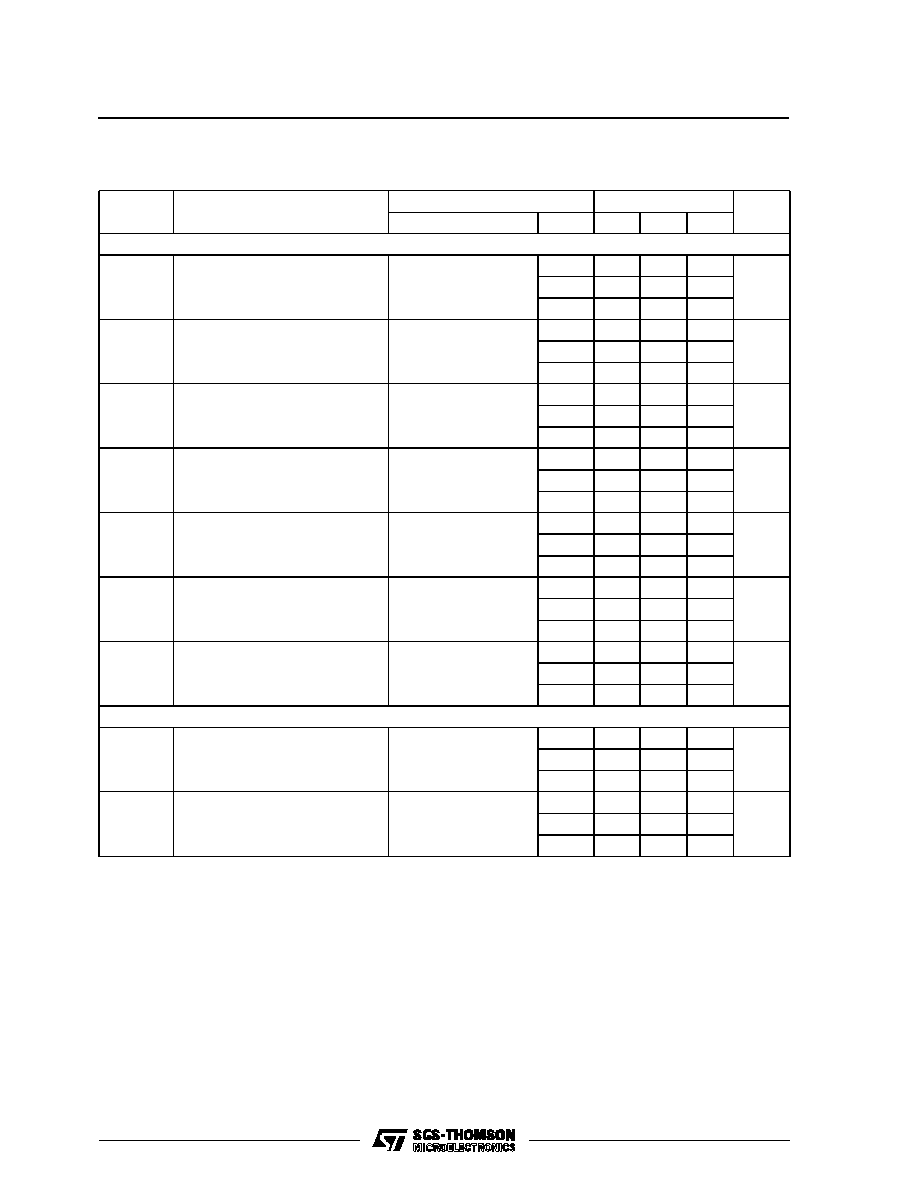
DYNAMIC ELECTRICAL CHARACTERISTICS (T
amb
= 25
∞
C, C
L
= 50pF, R
L
= 200k
,
typical temperature coefficient for all V
DD
= 0.3%/
∞
C, all input rise and fall time = 20ns)
Test Conditions
Val ue
Symbol
Parameter
V
D D
(V)
Min.
Typ.
Max.
Unit
CLOCKED OPERATI ON
t
PL H
, t
PHL
Propagation Delay Time
5
250
500
ns
10
100
200
15
75
150
t
T HL
, t
TL H
Transition Time
5
100
200
ns
10
50
100
15
40
80
f
CL
Maximum Clock Input Frequency
5
2
4
MHz
10
6
12
15
8
16
t
W
Clock Pulse Width
5
100
200
ns
10
45
90
15
30
60
t
r
, t
f
Clock Input Rise or Fall Time
5
15
µ
s
10
15
15
15
t
s e t u p
Data Setup Time J/K Lines
5
110
220
ns
10
40
80
15
30
60
t
s e t u p
Data Setup Time Parallel-In-Lines
5
70
140
ns
10
25
50
15
20
40
RESET OPERATION
t
PL H
, t
PHL
Propagation Delay Time
5
230
460
ns
10
100
200
15
80
160
t
W
Reset Pulse Width
5
125
250
ns
10
55
110
15
40
40
HCC/HCF4035B
5/14
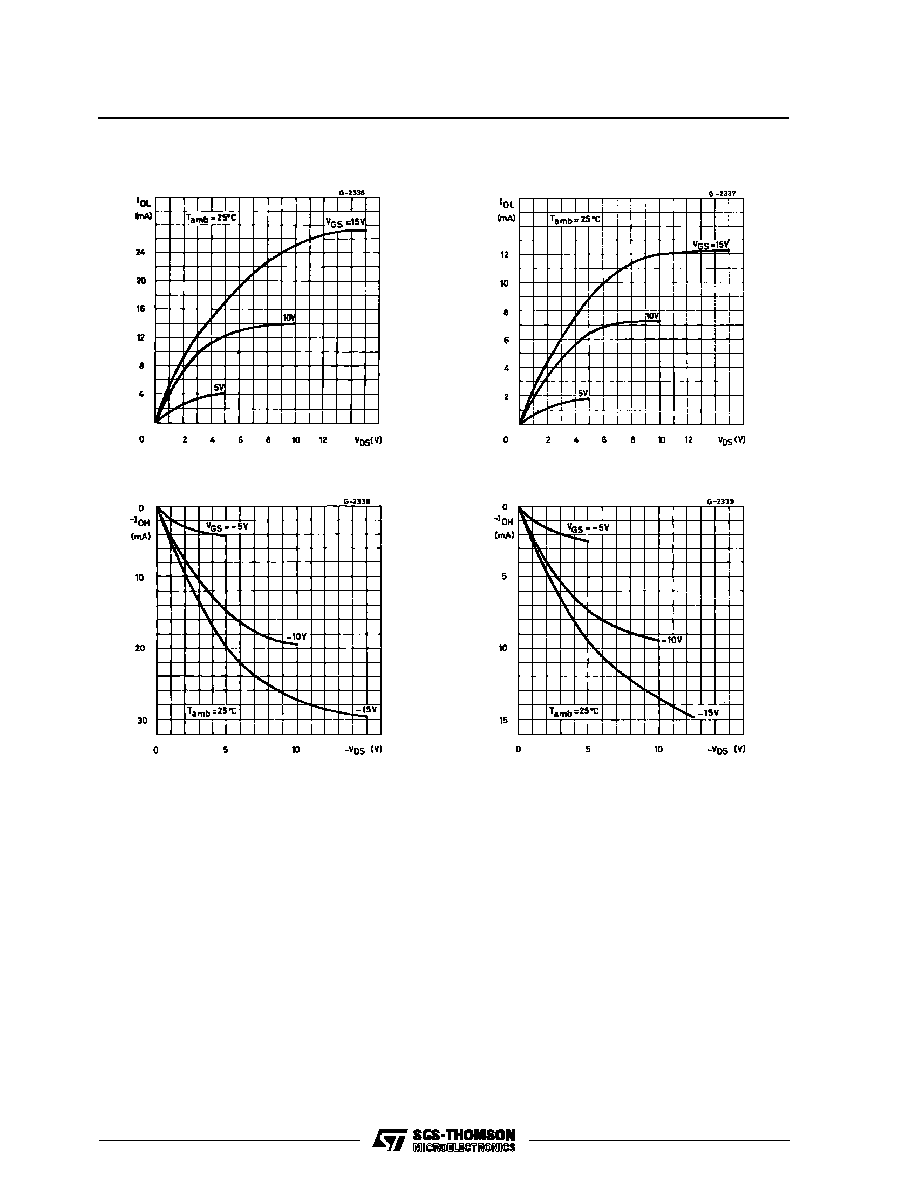
Typical Output High (source) Current Charac-
teristics.
Minimum Output High (source) Current Charac-
teristics.
Typical Output Low (sink) Current Characteristics.
Minimum Output Low (sink) Current Charac-
teristics.
HCC/HCF4035B
6/14
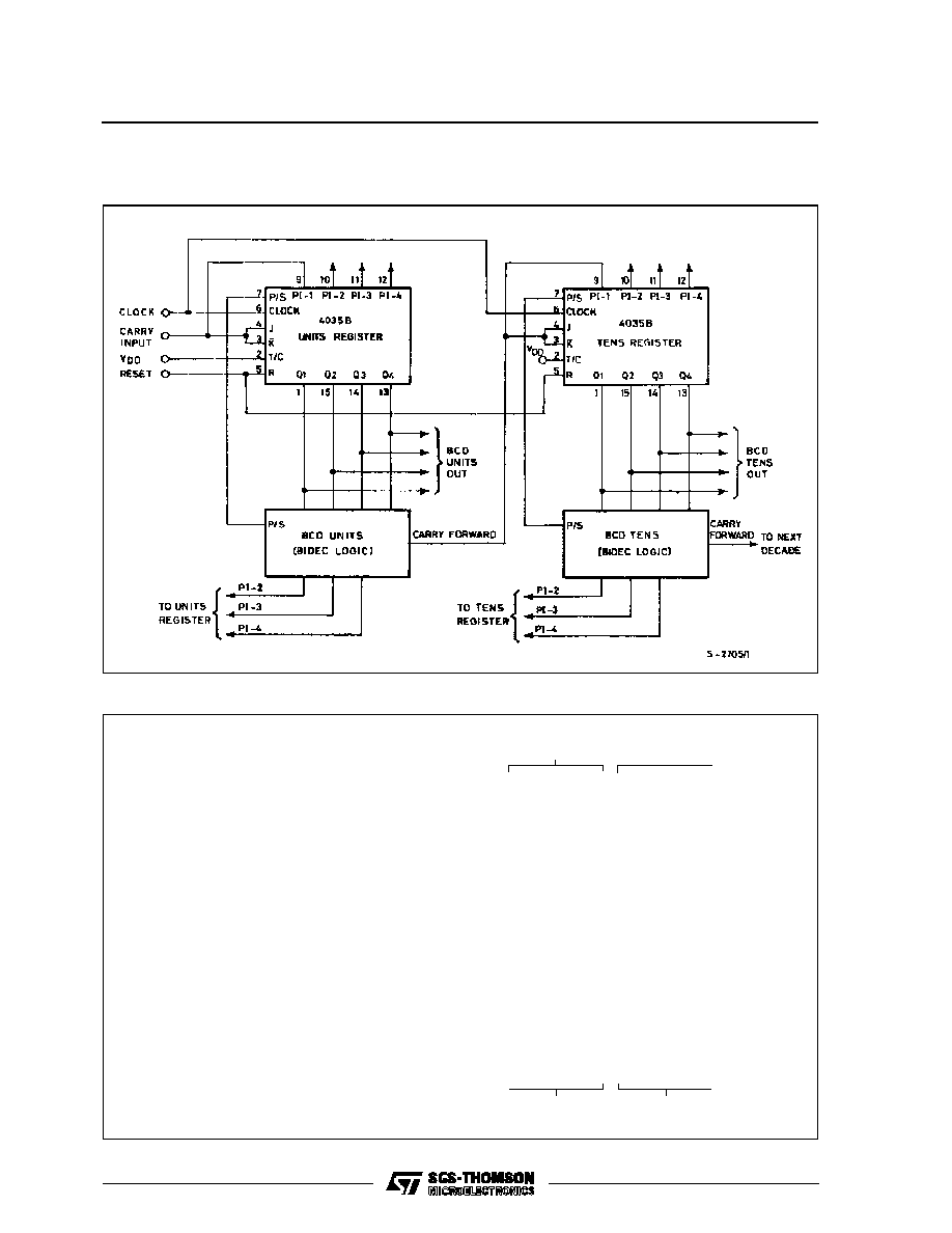
EXAMPLE OF BINARY-TO-BCD CONVERSION
BINARY-TO-BCD CONVERTER
Units
Tens
Register
Register
1
2
4
8
1
2
4
8
58 = 0
1
0
1
1
1
Shift
Shift
0
1
0
1
1
1
Shift
0
1
0
1
1
1
Add * 3 to Unit Decade & Shift
1
1
0
1
0
0
1
0
1
Shift
0
1
0
0
1
0
1
Add * 3 Units Decade & Shift
1
1
0
0
0
1
1
0
1
0
* From Left to Right
8
5
TYPICAL APPLICATIONS
LSB
MSB
HCC/HCF4035B
7/14

BIDEC LOGIC
DOUBLE SEQUENCE GENERATOR
STATE SEQUENCES
Control = E = 0
1
0
1
2
5
10
4
9
3
6
13
11
7
14
12
8
Q
1
A
0
1
0
1
0
0
1
1
0
1
1
1
0
0
0
Q
2
B
0
0
1
0
1
0
0
1
1
0
1
1
1
0
0
Q
3
C
0
0
0
1
0
1
0
0
1
1
0
1
1
1
0
Q
4
D
0
0
0
0
1
0
1
0
0
1
1
0
1
1
1
15
14
13
10
5
11
6
12
9
2
4
8
1
3
7
Q
1
A
1
0
1
0
1
1
0
0
1
0
0
0
1
1
1
Q
2
B
1
0
0
1
0
1
1
0
0
1
0
0
0
1
1
Q
3
C
1
1
1
0
1
0
1
1
0
0
1
0
0
0
1
Q
4
D
1
1
1
1
0
1
0
1
1
0
0
1
0
0
0
Using a control line (E) two different state se-
quences can be generated. For example, suppose
the following two sequences are desired on com-
mand (control line E).
TYPICAL APPLICATIONS
HCC/HCF4035B
8/14
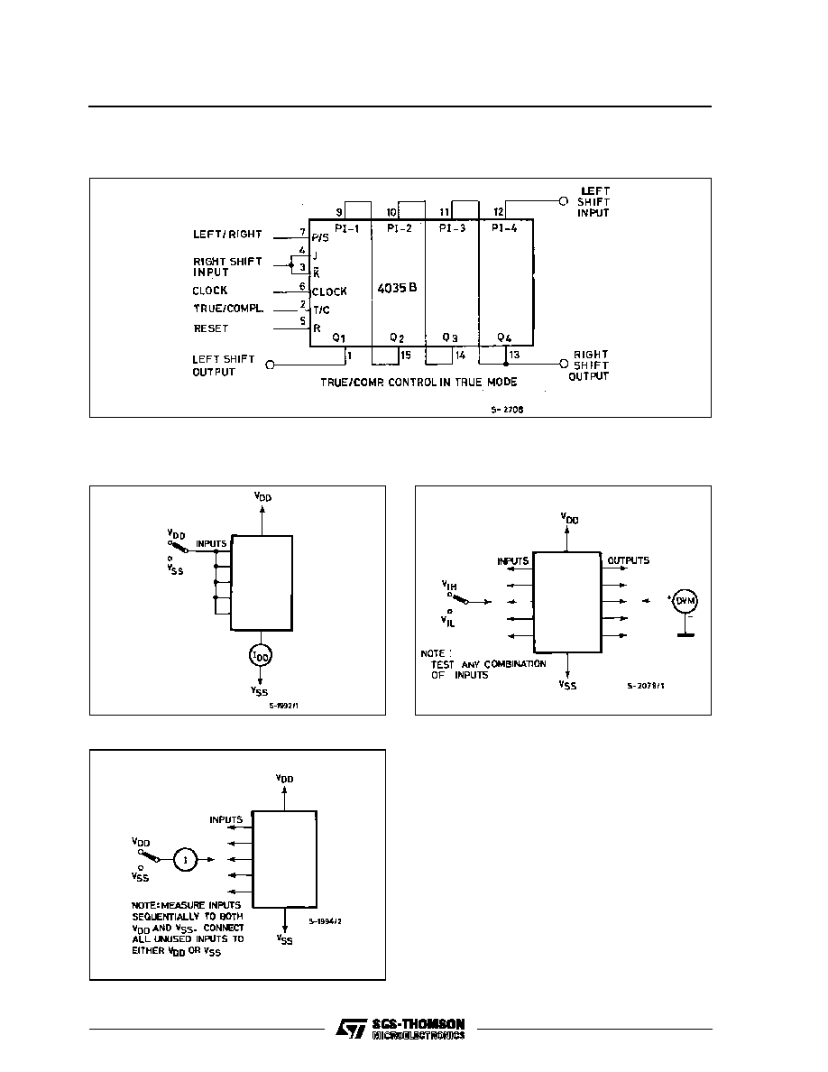
Input Current.
TEST CIRCUITS
Quiescent Device Current.
Input Voltage.
SHIFT LEFT/SHIFT RIGHT REGISTER
TYPICAL APPLICATIONS
HCC/HCF4035B
9/14
Plastic DIP16 (0.25) MECHANICAL DATA
DIM.
mm
inch
MIN.
TYP.
MAX.
MIN.
TYP.
MAX.
a1
0.51
0.020
B
0.77
1.65
0.030
0.065
b
0.5
0.020
b1
0.25
0.010
D
20
0.787
E
8.5
0.335
e
2.54
0.100
e3
17.78
0.700
F
7.1
0.280
I
5.1
0.201
L
3.3
0.130
Z
1.27
0.050
P001C
HCC/HCF4035B
10/14

Ceramic DIP16/1 MECHANICAL DATA
DIM.
mm
inch
MIN.
TYP.
MAX.
MIN.
TYP.
MAX.
A
20
0.787
B
7
0.276
D
3.3
0.130
E
0.38
0.015
e3
17.78
0.700
F
2.29
2.79
0.090
0.110
G
0.4
0.55
0.016
0.022
H
1.17
1.52
0.046
0.060
L
0.22
0.31
0.009
0.012
M
0.51
1.27
0.020
0.050
N
10.3
0.406
P
7.8
8.05
0.307
0.317
Q
5.08
0.200
P053D
HCC/HCF4035B
11/14
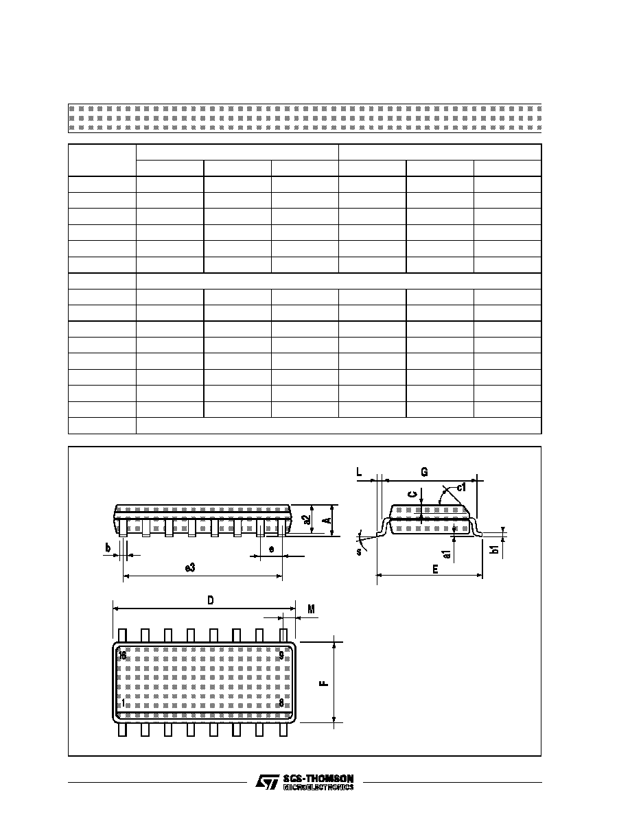
SO16 (Narrow) MECHANICAL DATA
DIM.
mm
inch
MIN.
TYP.
MAX.
MIN.
TYP.
MAX.
A
1.75
0.068
a1
0.1
0.2
0.004
0.007
a2
1.65
0.064
b
0.35
0.46
0.013
0.018
b1
0.19
0.25
0.007
0.010
C
0.5
0.019
c1
45
∞
(typ.)
D
9.8
10
0.385
0.393
E
5.8
6.2
0.228
0.244
e
1.27
0.050
e3
8.89
0.350
F
3.8
4.0
0.149
0.157
G
4.6
5.3
0.181
0.208
L
0.5
1.27
0.019
0.050
M
0.62
0.024
S
8
∞
(max.)
P013H
HCC/HCF4035B
12/14

PLCC20 MECHANICAL DATA
DIM.
mm
inch
MIN.
TYP.
MAX.
MIN.
TYP.
MAX.
A
9.78
10.03
0.385
0.395
B
8.89
9.04
0.350
0.356
D
4.2
4.57
0.165
0.180
d1
2.54
0.100
d2
0.56
0.022
E
7.37
8.38
0.290
0.330
e
1.27
0.050
e3
5.08
0.200
F
0.38
0.015
G
0.101
0.004
M
1.27
0.050
M1
1.14
0.045
P027A
HCC/HCF4035B
13/14

Information furnished is believed to be accurate and reliable. However, SGS-THOMSON Microelectronics assumes no responsability for the
consequences of use of such information nor for any infringement of patents or other rights of third parties which may results from its use. No
license is granted by implication or otherwise under any patent or patent rights of SGS-THOMSON Microelectronics. Specifications mentioned
in this publication are subject to change without notice. This publication supersedes and replaces all information previously supplied.
SGS-THOMSON Microelectronics products are not authorized for use as critical components in life support devices or systems without express
written approval of SGS-THOMSON Microelectonics.
©
1994 SGS-THOMSON Microelectronics - All Rights Reserved
SGS-THOMSON Microelectronics GROUP OF COMPANIES
Australia - Brazil - France - Germany - Hong Kong - Italy - Japan - Korea - Malaysia - Malta - Morocco - The Netherlands -
Singapore - Spain - Sweden - Switzerland - Taiwan - Thailand - United Kingdom - U.S.A
HCC/HCF4035B
14/14