HCC/HCF4046B
MICROPOWER PHASE-LOCKED LOOP
.
QUIESCENT CURRENT SPECIFIED TO 20V
FOR HCC DEVICE
.
VERY LOW POWER CONSUMPTION : 100
µ
W
(TYP.) AT VCO f
o
= 10kHz, V
DD
= 5V
.
OPERATING FREQUENCY RANGE : UP TO
1.4MHz (TYP.) AT V
DD
= 10V
.
LOW FREQUENCY DRIFT : 0.06%/
∞
C (typ.) AT
V
DD
= 10V
.
CHOICE OF TWO PHASE COMPARATORS :
1) EXCLUSIVE - OR NETWORK
2) EDGE-CONTROLLED MEMORY NETWORK
WITH PHASE-PULSE OUTPUT FOR LOCK IN-
DICATION
.
HIGH VCO LINEARITY : 1% (TYP.)
.
VCO INHIBIT CONTROL FOR ON-OFF KE-
YING AND ULTRA-LOW STANDBY POWER
CONSUMPTION
.
SOURCE-FOLLOWER
OUTPUT
OF
VCO
CONTROL INPUT (demod. output)
.
ZENER DIODE TO ASSIST SUPPLY REGULA-
TION
.
5V, 10V AND 15V PARAMETRIC RATING
.
INPUT CURRENT OF 100nA AT 18V AND 25
∞
C
FOR HCC DEVICE
.
100% TESTED FOR QUIESCENT CURRENT
.
MEETS ALL REQUIREMENTS OF JEDEC TEN-
TATIVE STANDARD N
∞
. 13A, "STANDARD
SPECIFICATIONS FOR DESCRIPTION OF "B"
SERIES CMOS DEVICES"
June 1989
The HCC4046B (extended temperature range) and
HCF4046B (intermediate temperature range) are
monolithic integrated circuits, available in 16-lead
dual in-line plastic or ceramic package. The
HCC/HCF4046B COS/MOS Micropower Phase-
Locked Loop (PLL) consists of a low-power, linear
voltage-controlled oscillator (VCO) and two different
phase comparators having a common signal-input
amplifier and a common comparator input. A 5.2V
zener diode is provided for supply regulation if
necessary.
EY
(Plastic Package)
F
(Ceramic Package)
C1
(Chip Carrier)
ORDER CODES :
HCC4046BF
HCF4046BEY
HCF4043BC1
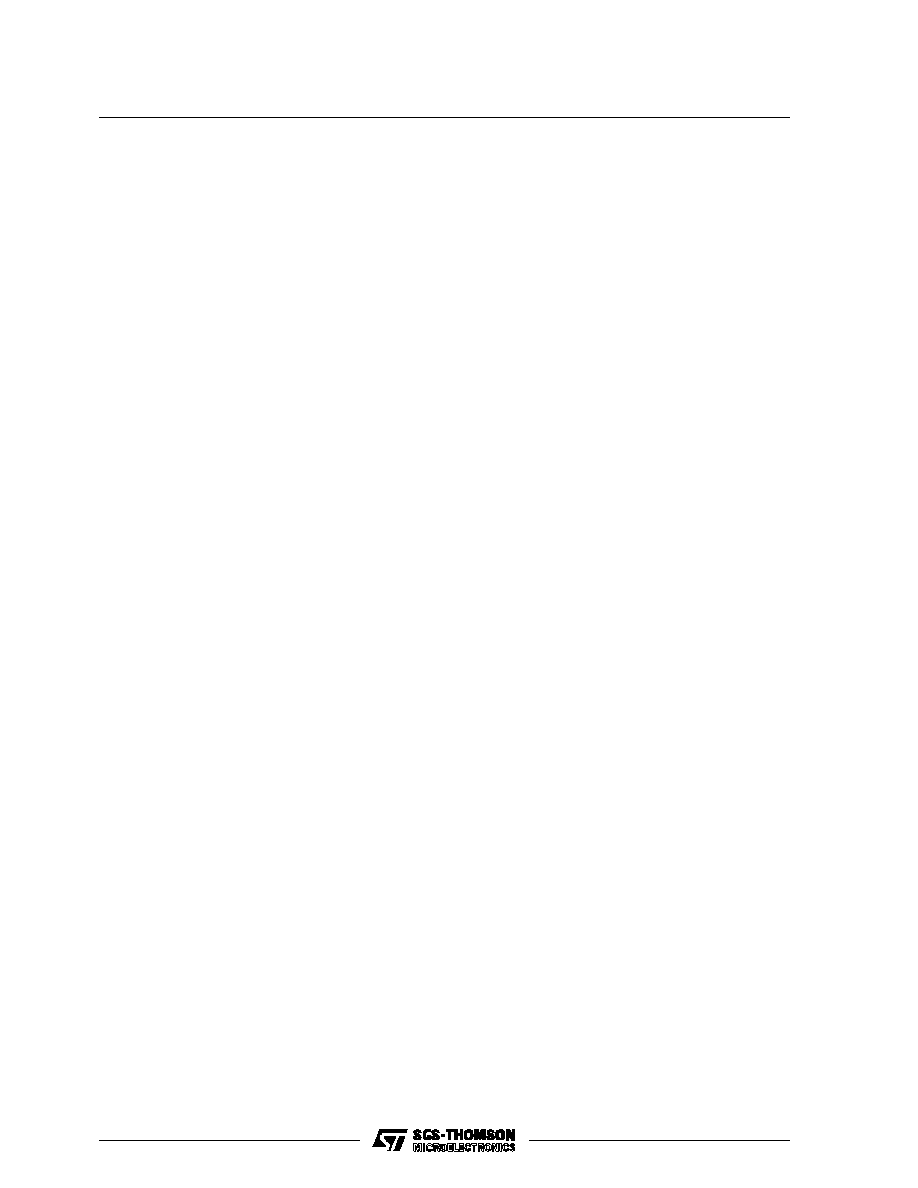
PIN CONNECTIONS
DESCRIPTION
1/13
VCO Section
The VCO requires one external capacitor C1 and
one or two external resistors (R1 or R1 and R2). Re-
sistor R1 and capacitor C1 determine the frequency
range of the VCO and resistor R2 enables the VCO
to have a frequency offset if required. The high input
impedance (10
12
) of the VCO simplifiers the design
of low-pass filters by permitting the designer a wide
choice of resistor-to-capacitor ratios. In order not to
load the low-pass filter, a source-follower output of the
VCO input voltage is provided at terminal 10 (DE-
MODULATED OUTPUT). If this terminal is used, a
load resistor (R
S
) of 10 k
or more should be con-
nected from this terminal to V
SS
. If unused this termi-
nal should be left open. The VCO can be connected
either directly or through frequency dividers to the
comparator input of the phase comparators. A full
COS/MOSlogic swing is available at the output of the
VCO and allows direct coupling to COS/MOS fre-
quency dividers such as the HCC/HCF4024B,
HCC/HCF4018B, HCC/HCF4020B,
HCC/HCF4022B, HCC/HCF4029B,and
HBC/HBF4059A. One or more HCC/HCF4018B
(Presettable Divide-by-N Counter) or HCC/HCF4029B
(Presettable Up/Down Counter), or HBC/HBF4059A
(Programmable Divide-by-"N" Counter), together
with the HCC/HCF4046B (Phase-Locked Loop) can
be used to build a micropower low-frequency syn-
thesizer. A logic 0 on the INHIBIT input "enables" the
VCO and the source follower, while a logic 1 "turns
off" both to minimize stand-by power consumption.
Phase Comparators
The phase-comparator signal input (terminal 14)
can be direct-coupled provided the signal swing is
within COS/MOS logic levels [logic "0"
30 %
(V
DD
≠ V
SS
), logic "1"
70 % (V
DD
- V
SS
)]. For
smaller swings the signal must be capacitively
coupled to the self-biasing amplifier at the signal
input. Phase comparator I is an exclusive-OR net-
work ; it operates analagously to an over-driven bal-
anced mixer. To maximize the lock range, the
signal-and comparator-input frequencies must have
a 50% duty cycle. With no signal or noise on the sig-
nal input, this phase comparator has an average
output voltage equal to V
DD
/2. The low-pass filter
connected to the output of phase comparator I sup-
plies the averaged voltage to the VCO input, and
causes the VCO to oscillate at the center frequency
(f
o
). The frequency range of input signals on which
the PLL will lock if it was initially out of lock is defined
as the frequency capture range (2 f
c
). The frequency
range of input signals on which the loop will stay
locked if it was initially in lock is defined as the fre-
quency lock range (2 f
L
). The capture range is
the
lock range. With phase comparator I the range of
frequencies over which the PLL can acquire lock
(capture range) is dependent on the low-pass-filter
characteristics, and can be made as large as the
lock range. Phase-comparator I enables a PLL sys-
tem to remain in lock in spite of high amounts of
noise in the input signal. One characteristic of this
type of phase comparator is that it may lock onto
input frequencies that are close to harmonics of the
VCO center-frequency. A second characteristic is
that the phase angle between the signal and the
comparator input varies between 0
∞
and 180
∞
, and
is 90
∞
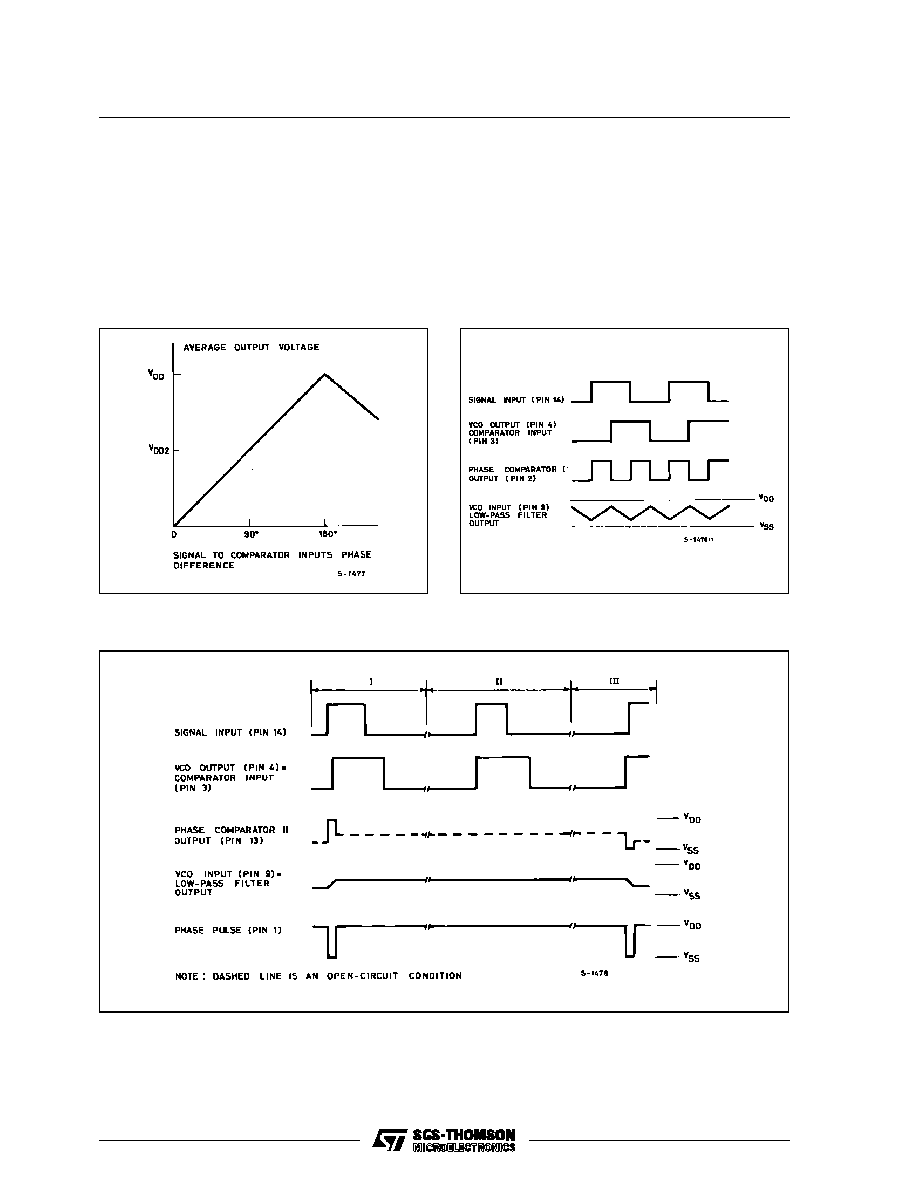
at the center frequency. Fig. (a) shows the
typical, triangular, phase-to-output response char-
acteristic of phase-comparator I. Typical waveforms
for a COS/MOS phase-locked-loop
employing
phase comparator I in locked condition of f
o
is shown
in fig. (b). Phase-comparator II is an edge-controlled
digital memory network. It consists of four flip-flop
stages, control gating, and a three-stage output-cir-
cuit comprising p- and n-type drivers having a com-
mon output node. When the p-MOS or n-MOS
drivers are ON they pull the output up to V
DD
or down
to V
SS
, respectively. This type of phase comparator
acts only on the positive edges of the signal and
comparator inputs. The duty cycles of the signal and
comparator inputs are not important since positive
transitions control the PLL system utilizing this type
of comparator. If the signal-input frequency is higher
than the comparator-input frequency, the p-type
output driver is maintained ON most of the time, and
both the n- and p-drivers OFF (3 state) the remain-
der of the time. If the signal-input frequency is lower
than the comparator-input frequency, the n-type
output driver is maintained ON most of the time, and
both the n- and p-drivers OFF (3 state) the remain-
der of the time. If the signal and comparator-input
frequencies are the same, but the signal input lags
the comparator input in phase, the n-type output
driver is maintained ON for a time corresponding to
the phase difference. If the signal and comparator-
input frequencies are the same, but the comparator
input lags the signal in phase, the p-type output
driver is maintained ON for a time corresponding to
the phase difference. Subsequently, the capacitor
voltage of the low-pass filter connected to this phase
comparator is adjusted until the signal and com-
parator inputs are equal in both phase and fre-
quency. At this stable point both p- and n-type output
drivers remain OFF and thus the phase comparator
output becomes an open circuit and holds the volt-
age on the capacitor of the low-pass filter constant.
Moreover the signal at the "phase pulses" output is
a high level which can be used for indicating a locked
condition. Thus, for phase comparator II, no phase
difference exists between signal and comparator
HCC/HCF4046B
2/13
input over the full VCO frequency range. Moreover,
the power dissipation due to the low-pass filter is re-
duced when this type of phase comparator is used
because both the p- and n-type output drivers are
OFF for most of the signal input cycle. It should be
noted that the PLL lock range for this type of phase
comparator is equal to the capture range, inde-
pendent of the low-pass filter. With no signal present
at the signal input, the VCO is adjusted to its lowest
frequency for phase comparator II. Fig. (c) shows
typical waveforms for a COS/MOS PLL employing
phase comparator II in a locked condition.
Figure a : Phase-Comparator I Characteristics at
Low-Pass Filter Output.
Figure b : Typical Waveforms for COS/MOS Phase
Locked-Loop Employing Phase Com-
parator I in Locked Condition of f
o.
Figure C : Typical Waveforms For COS/MOS Phase-locked Loop Employing Phase Comparator II In
Locked Condition.
HCC/HCF4046B
3/13
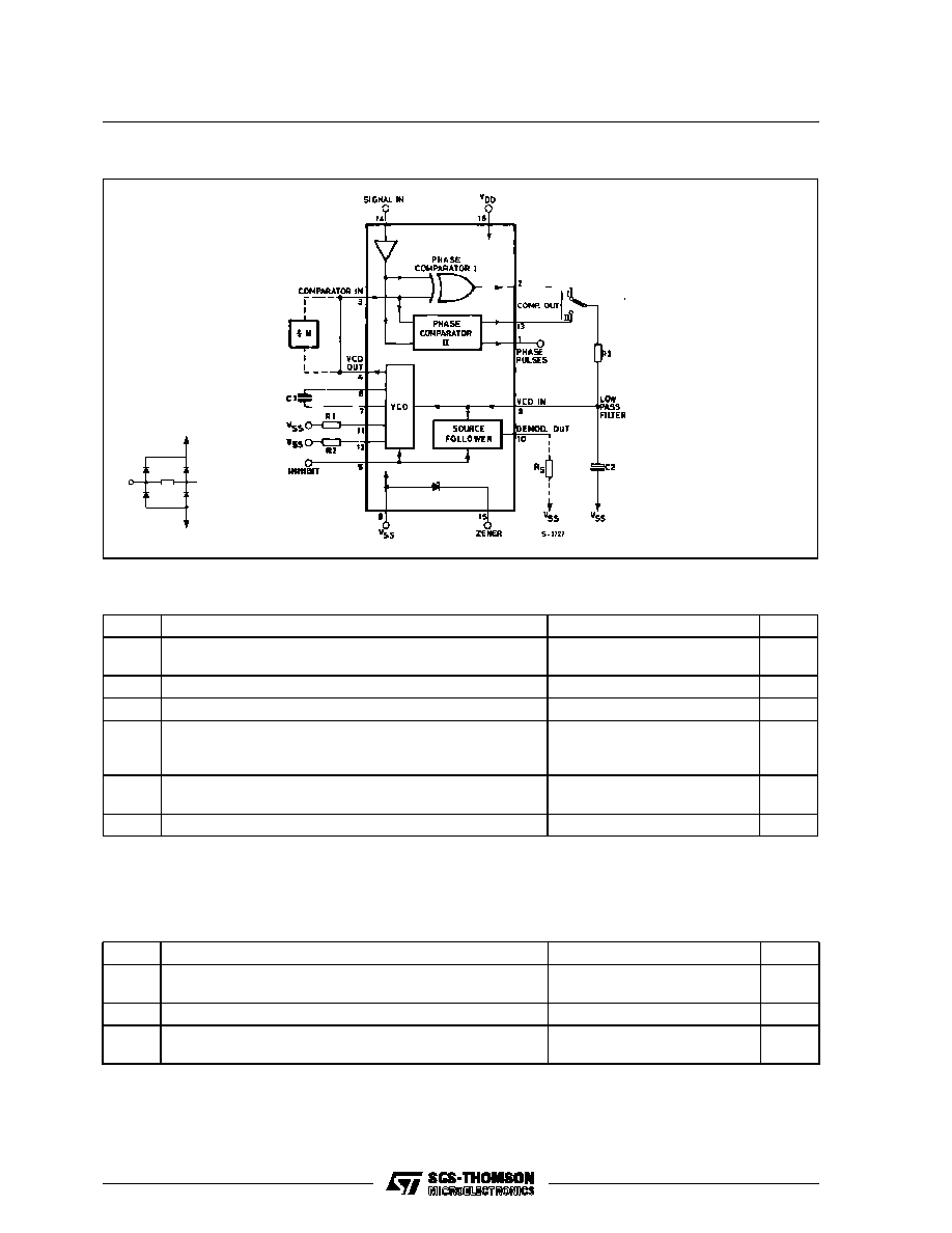
FUNCTIONAL DIAGRAM
ABSOLUTE MAXIMUM RATINGS
Symbol
Parameter
Value
Unit
V
DD
*
Supply Voltage : HC C Types
H C F Types
≠ 0.5 to + 20
≠ 0.5 to + 18
V
V
V
i
Input Voltage
≠ 0.5 to V
DD
+ 0.5
V
I
I
DC Input Current (any one input)
±
10
mA
P
t o t
Total Power Dissipation (per package)
Dissipation per Output Transistor
for T
o p
= Full Package-temperature Range
200
100
mW
mW
T
o p
Operating Temperature : HCC Types
H CF Types
≠ 55 to + 125
≠ 40 to + 85
∞
C
∞
C
T
s t g
Storage Temperature
≠ 65 to + 150
∞
C
RECOMMENDED OPERATING CONDITIONS
Symbol
Parameter
Value
Unit
V
DD
Supply Voltage : HC C Types
H C F Types
3 to 18
3 to 15
V
V
V
I
Input Voltage
0 to V
DD
V
T
o p
Operating Temperature : H CC Types
H C F Types
≠ 55 to + 125
≠ 40 to + 85
∞
C
∞
C
Stresses above those listed under "Absolute Maximum Ratings" may cause permanent damage to the device. This is a stress rating only
and functional operation of the device at these or any other conditions above those indicated in the operational sections of this specification
is not implied. Exposure to absolute maximum rating conditions for external periods may affect device reliability.
* All voltage values are referred to V
SS
pin voltage.
V
DD
SS
V
S-2299
ALL INPUTS ARE PROTECTED BY
COS/MOS PROTECTION NETWORK
HCC/HCF4046B
4/13
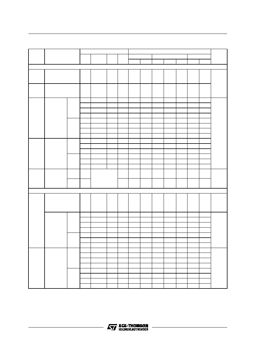
STATIC ELECTRICAL CHARACTERISTICS (over recommended operating conditions)
Test Conditions
Value
V
I
V
O
|I
O
|
V
D D
T
L o w
*
25
∞
C
T
Hi g h
*
Symbol
Parameter
(V)
(V)
(
µ
A)
(V)
Min. Max. Min.
Typ. Max. Min. Max.
Unit
V CO SECTI ON
V
O H
Output High
Voltage
0/ 5
0/10
0/15
< 1
< 1
< 1
5
10
15
4.95
9.95
14.95
4.95
9.95
14.95
5
10
15
4.95
9.95
14.95
V
V
O L
Output Low
Voltage
5/0
10/0
15/0
< 1
< 1
< 1
5
10
15
0.05
0.05
0.05
0.05
0.05
0.05
0.05
0.05
0.05
I
O H
Output
Drive
Current
HCC
Types
0/ 5
2.5
5
≠ 2
≠ 1.6 ≠ 3.2
≠ 1.15
mA
0/ 5
4.6
5
≠ 0.64
≠ 0.51
≠ 1
≠ 0.36
0/10
9.5
10
≠ 1.6
≠ 1.3 ≠ 2.6
≠ 0.9
0/15
13.5
15
≠ 4.2
≠ 3.4 ≠ 6.8
≠ 2.4
HCF
Types
0/ 5
2.5
5
≠ 1.53
≠ 1.36 ≠ 3.2
≠ 1.1
0/ 5
4.6
5
≠ 0.52
≠ 0.44
≠ 1
≠ 0.36
0/10
9.5
10
≠ 1.3
≠ 1.1 ≠ 2.6
≠ 0.9
0/15
13.5
15
≠ 3.6
≠ 3.0 ≠ 6.8
≠ 2.4
I
O L
Output
Sink
Current
HCC
Types
0/ 5
0.4
5
0.64
0.51
1
0.36
0/10
0.5
10
1.6
1.3
2.6
0.9
0/15
1.5
15
4.2
3.4
6.8
2.4
HCF
Types
0/ 5
0.4
5
0.52
0.44
1
0.36
0/10
0.5
10
1.3
1.1
2.6
0.9
0/15
1.5
15
3.6
3.0
6.8
2.4
I
IH
, I
IL
Input
Leakage
Current
HCC
Types
0/18
Any Input
18
±
0.1
±
10
≠ 5
±
0.1
±
1
µ
A
HCF
Types
0/15
15
±
0.3
±
10
≠ 5
±
0.3
±
1
PHASE COMPARATOR SECTI ON
I
DD
Total Device
Current
Pin 14 = Open
Pin 5 = V
DD
0/ 5
0/10
0/15
0/20
5
10
15
20
0.1
0.5
1.5
4
0.05
0.25
0.75
2
0.1
0.5
1.5
4
0.1
0.5
1.5
4
mA
Pin
14 =V
SS
or V
DD
Pin 5 = V
DD
HCC
Types
0/ 5
5
5
0.04
5
150
µ
A
0/10
10
10
0.04
10
300
0/15
15
20
0.04
20
600
0/20
20
100
0.08
100
3000
HCF
Types
0/ 5
5
20
0.04
20
150
0/10
10
40
0.04
40
300
0/15
15
80
0.04
80
600
I
O H
Output
Drive
Current
HCC
Types
0/ 5
2.5
5
≠ 2
≠ 1.6 ≠ 3.2
≠ 1.15
mA
0/ 5
4.6
5
≠ 0.64
≠ 0.51
≠ 1
≠ 0.36
0/10
9.5
10
≠ 1.6
≠ 1.3 ≠ 2.6
≠ 0.9
0/15
13.5
15
≠ 4.2
≠ 3.4 ≠ 6.8
≠ 2.4
HCF
Types
0/ 5
2.5
5
≠ 1.53
≠ 1.36 ≠ 3.2
≠ 1.1
0/ 5
4.6
5
≠ 0.52
≠ 0.44
≠ 1
≠ 0.36
0/10
9.5
10
≠ 1.3
≠ 1.1 ≠ 2.6
≠ 0.9
0/15
13.5
15
≠ 3.6
≠ 3.0 ≠ 6.8
≠ 2.4
* T
Low
= ≠ 55
∞
C for HCC device : ≠ 40
∞
C for HCF device.
* T
High
= + 125
∞
C for HCC device : + 85
∞
C for HCF device.
The Noise Margin for both "1" and "0" level is : 1V min. with V
DD
= 5V, 2V min. with V
DD
= 10V, 2.5V min. with V
DD
= 15V.
HCC/HCF4046B
5/13