HCC/HCF4049UB
HCC/HCF4050B
HEX BUFFER/CONVERTERS
DESCRIPTION
.
HIGH SINK CURRENT FOR DRIVING 2 TTL
LOADS
.
HIGH-TO-LOW LEVEL LOGIC CONVERSION
.
QUIESCENT CURRENT SPECIFIED TO 20V
FOR HCC DEVICE
.
HIGH "SINK" AND "SOURCE" CURRENT CA-
PABILITY
.
5V, 10V AND 15V PARAMETRIC RATINGS
.
INPUT CURRENT OF 100 nA AT 18V AND 25
∞
C
FOR HCC DEVICE
.
100% TESTED FOR QUIESCENT CURRENT
.
MEETS ALL REQUIREMENTS OF JEDEC TEN-
TATIVE STANDARD N
o
. 13A, "STANDARD
SPECIFICATIONS FOR DESCRIPTION OF "B"
SERIES CMOS DEVICES"
June 1989
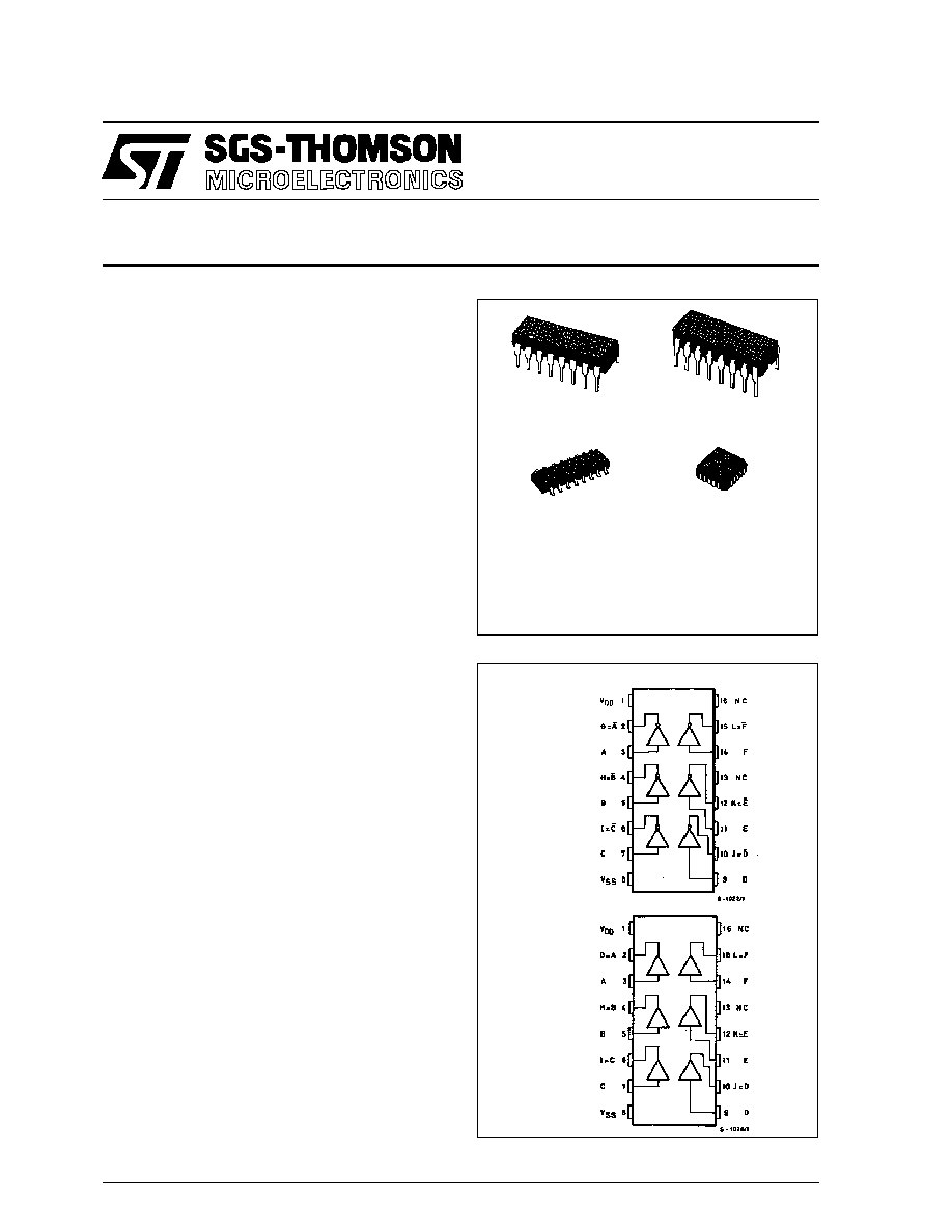
The HCC4049UB/4050B (extended temperature
range) and the HCF4049UB/4050B (intermediate
temperature range) are monolithic integrated cir-
cuits available in 16-lead dual in-line plastic or ce-
ramic package and plastic micro package.
The HCC/HCF4049UB/4050B are inverting and
non-inverting hex buffers, respectively, and feature
logic-level conversion using only one supply voltage
(V
DD
). The input-signal high level (V
IH
) can exceed
the V
DD
supply voltage when these devices are used
for logic level conversions. These devices are in-
tended for use as COS/MOS to DTL/TTL converters
and can drive directly two DTL/TTL loads (V
DD
= 5V,
V
OL
0.4V, and I
OL
3.2mA).
EY
(Plastic Package)
F
(Ceramic Frit Seal Package)
M1
(Micro Package)
ORDER CODES :
HCC40XXBF
HCF40XXBM1
HCF40XXBEY
HCF40XXBC1
PIN CONNECTIONS
4049UB
INVERTING TYPE
4050B
NON-INVERTING TYPE
4049UB
4050B
C1
(Plastic Chip Carrier)
1/12
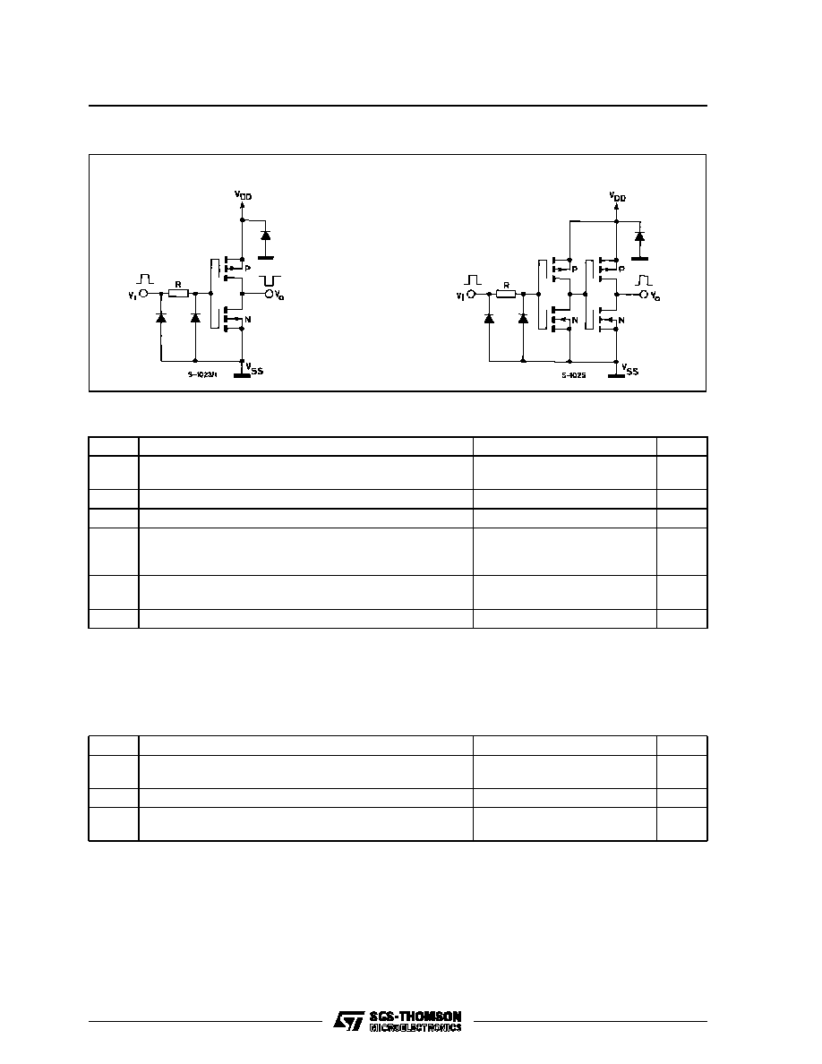
SCHEMATIC DIAGRAMS (1 of 6 identical units)
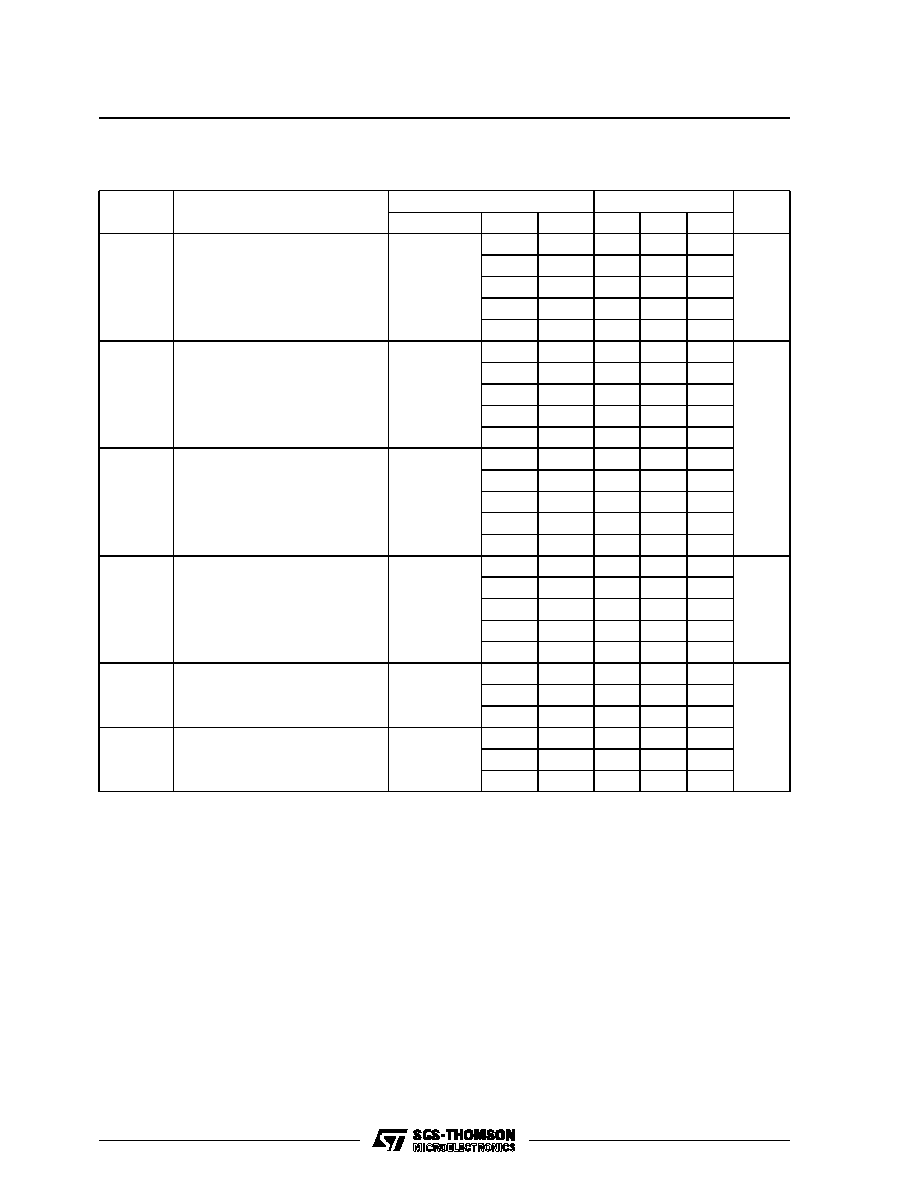
ABSOLUTE MAXIMUM RATINGS
Symbol
Parameter
Value
Unit
V
DD
*
Supply Voltage : HC C Types
H C F Types
≠ 0.5 to + 20
≠ 0.5 to + 18
V
V
V
i
Input Voltage
≠ 0.5 to V
DD
+ 0.5
V
I
I
DC Input Current (any one input)
±
10
mA
P
t o t
Total Power Dissipation (per package)
Dissipation per Output Transistor
for T
o p
= Full Package-temperature Range
200
100
mW
mW
T
o p
Operating Temperature : HCC Types
H CF Types
≠ 55 to + 125
≠ 40 to + 85
∞
C
∞
C
T
s t g
Storage Temperature
≠ 65 to + 150
∞
C
RECOMMENDED OPERATING CONDITIONS
Symbol
Parameter
Value
Unit
V
DD
Supply Voltage : HC C Types
H C F Types
3 to 18
3 to 15
V
V
V
I
Input Voltage
0 to V
DD
V
T
o p
Operating Temperature : H CC Types
H C F Types
≠ 55 to + 125
≠ 40 to + 85
∞
C
∞
C
4049UB
4050B
Stresses above those listed under "Absolute Maximum Ratings" may cause permanent damage to the device. This is a stress
rating only and functional operation of the device at these or any other conditions above those indicated in the operational sec-
tions of this specifi cation is not implied. Exposure to absolute maximum rating conditions for external periods may affect device
reliability.
* All voltage values are referred to V
SS
pin voltage.
HCC/HCF4049UB/4050B
2/12

STATIC ELECTRICAL CHARACTERISTICS (over recommended operating conditions)
Test Conditions
Val ue
Symbol
Parameter
V
I
V
O
V
DD
T
Lo w
*
25
∞
C
T
High
*
Unit
(V)
(V)
(V)
Min.
Max.
Min.
Typ.
Max.
Min.
Max.
I
L
Quiescent
Supply
Current
HCC
Types
0/ 5
5
1
0.02
1
30
µ
A
0/10
10
2
0.02
2
60
0/15
15
4
0.02
4
120
0/20
20
20
0.04
20
600
HCF
Types
0/ 5
5
4
0.02
4
30
0/10
10
8
0.02
8
60
0/15
15
16
0.02
16
120
V
OH
Output High
Voltage
0/ 5
5
4.95
4.95
4.95
V
0/10
10
9.95
9.95
9.95
0/15
15
14.95
14.95
14.95
V
OL
Output Low
Voltage
5/0
5
0.05
0.05
0.05
V
10/0
10
0.05
0.05
0.05
15/0
15
0.05
0.05
0.05
V
IH
Input High
Voltage (4049UB)
0.5
5
4
4
4
V
1
10
8
8
8
2
15
12
12
12
V
IH
Input High
Voltage (4050B)
4.5
5
3.5
3.5
3.5
V
9
10
7
7
7
13.5
16
11
11
11
V
IL
Input Low
Voltage (4049UB)
4.5
5
1
1
1
V
9
10
2
2
2
13
15
3
3
3
V
IL
Input Low
Voltage (4050B)
0.5
5
1.5
1.5
1.5
V
1
10
3
3
3
1.5
15
4
4
4
I
OH
Output
Drive
Current
HCC
Types
0/ 5
2.5
5
1.6
≠1.25 ≠ 6.4
≠ 0.9
mA
0/ 5
4.6
5
0.64
≠0.51 ≠ 1.6
≠0.36
0/10
9.5
10
1.6
≠1.30 ≠ 3.6
≠ 0.9
0/15
13.5
15
4.7
≠3.75 ≠ 12
≠ 2.7
HCF
Types
0/ 5
2.5
5
1.5
≠1.25 ≠ 6.4
≠ 1
0/ 5
4.6
5
0.61
≠0.51 ≠ 1.6
≠0.42
0/10
9.5
10
1.5
≠1.25 ≠ 3.6
≠ 1
0/15
13.5
15
4.5
≠3.75 ≠ 12
≠ 3
I
OL
Output
Sink
Current
HCC
Types
0/ 5
0.4
5
3.75
3.2
6.4
2.2
mA
0/10
0.5
10
10
8
16
5.6
0/15
1.5
15
30
24
48
17
HCF
Types
0/ 5
0.4
5
3.6
3.2
6.4
2.6
0/10
0.5
10
9.6
8
16
6.6
0/15
1.5
15
28
24
48
19
I
IH
, I
IL
Input
Leakage
Current
HCC
Types
0/18
18
±
0. 1
±
10
≠5
±
0.1
±
1
µ
A
HCF
Types
0/15
15
±
0. 3
±
10
≠5
±
0.3
±
1
C
I
Input
Capacitance
4049UB
4050B
Any Input
15
5
22.5
7.5
pF
(*) T
Low
= ≠ 55
∞
C for HCC device : ≠ 40
∞
C for HCF device.
T
High
=
+ 125
∞
C for HCC device : + 85
∞
C for HCF device.
The Noise Margin (only HCC/HCF4050B type) for both "1" and "0" level is : 1V min. with V
DD
= 5V, 2V min. with V
DD
= 10V,
2.5V min. with V
DD
= 15V.
HCC/HCF4049UB/4050B
3/12
DYNAMIC ELECTRICAL CHARACTERISTICS (T
amb
= 25
∞
C, C
L
= 50pF, R
L
= 200k
,
typical temperature coefficient for all V
DD
values is 0.3%/
∞
C, all input rise and fall times = 20ns)
Test Conditions
Val ue
Symbol
Parameter
V
I
(V)
V
D D
(V)
Min.
Typ.
Max.
Unit
t
PL H
Propagation Delay Time
(4049UB)
5
5
60
120
ns
10
10
32
65
10
5
45
90
15
15
25
50
15
5
45
90
t
PL H
Propagation Delay Time
(4050B)
5
5
70
140
ns
10
10
40
80
10
5
45
90
15
15
30
60
15
5
40
80
t
PHL
Propagation delay Time
(4049UB)
5
5
32
65
10
10
20
40
10
5
15
30
15
15
15
30
15
5
10
20
t
PHL
Propagation Delay Time
(4050B)
5
5
55
110
ns
10
10
22
55
10
5
50
100
15
15
15
30
15
5
50
100
t
T L H
Transition Time
5
5
80
160
ns
10
10
40
80
15
15
30
60
t
T HL
Transition Time
5
5
30
60
10
10
20
40
15
15
15
30
HCC/HCF4049UB/4050B
4/12
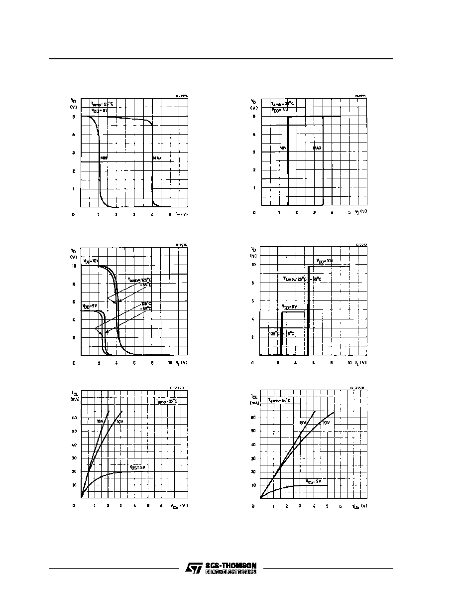
Minimum and Maximum Voltage Transfer Charac-
teristics for 4049UB.
Minimum and Maximum Voltage Transfer Charac-
teristics for 4050B.
Typical Voltage Transfer Characteristics as a Func-
tion of Temperature for 4049UB.
Typical Voltage Transfer Characteristics as a Func-
tion of Temperature for 4050B.
Typical Output Low (sink) Current Characteristics.
Minimum Output Low (sink) Current Characteristics.
HCC/HCF4049UB/4050B
5/12